Tag: Innovation

  • Hitachi Energy Fuels India’s AI Ambitions with ₹2,000 Crore Chennai Innovation Hub Expansion

    Hitachi Energy Fuels India’s AI Ambitions with ₹2,000 Crore Chennai Innovation Hub Expansion

    Chennai, India – October 15, 2025 – In a monumental boost for India's burgeoning technology landscape and the global push towards sustainable energy, Hitachi Energy today announced a substantial investment of ₹2,000 crore (approximately $250 million) to significantly expand its Global Technology and Innovation Centre in Chennai. This strategic move, unveiled on this very day, is poised to create an impressive 3,000 new, high-value technology jobs, further solidifying India's position as a critical hub for advanced research and development in the energy sector.

    The expansion underscores Hitachi Energy's commitment to accelerating innovation, digitalization, and engineering capabilities, with a keen focus on developing cutting-edge sustainable energy solutions. The Chennai centre, already a powerhouse employing over 2,500 energy transition technologists, is set to become an even more formidable strategic global hub, consolidating diverse engineering and R&D expertise to serve both India and the world.

    Powering Tomorrow: AI and Digitalization at the Core of Chennai's Expanded Hub

    The ₹2,000 crore investment is earmarked for a comprehensive upgrade and expansion of the Chennai facility, transforming it into a nexus for next-generation energy technologies. At the heart of this transformation lies an aggressive push into digitalization and advanced artificial intelligence (AI) applications. The centre's enhanced capabilities will span critical areas including advanced grid automation, high-voltage systems, HVDC (High Voltage Direct Current) technologies, and seamless grid integration, all underpinned by sophisticated AI and machine learning frameworks.

    A key differentiator for the expanded centre will be its focus on "cutting-edge projects like development of digital twins and advanced grid automation applications." Digital twins, virtual replicas of physical assets, leverage AI for real-time data analysis, predictive maintenance, and optimized operational performance, enabling unprecedented levels of efficiency and reliability in energy infrastructure. Similarly, advanced grid automation, powered by AI, promises intelligent control, proactive fault detection, and enhanced resilience for complex power grids. This forward-thinking approach significantly deviates from traditional, often reactive, energy management systems, ushering in an era of predictive and self-optimizing energy networks. Initial reactions from the AI research community and industry experts highlight this as a pivotal step towards integrating AI deeply into critical infrastructure, setting a new benchmark for industrial digitalization.

    Beyond core energy technologies, the centre will also bolster its expertise in cybersecurity, recognizing the paramount importance of protecting digitized energy systems from evolving threats. AI and machine learning will be instrumental in developing robust defense mechanisms, anomaly detection, and threat intelligence to safeguard national and international energy grids. The creation of 3,000 high-value, high-paying, hi-tech jobs signals a clear demand for professionals skilled in AI, data science, advanced analytics, and complex software engineering, further enriching India's talent pool in these critical domains. The centre's capacity to manage over 1,000 projects annually across 40 countries speaks volumes about its global strategic importance.

    Competitive Edge and Market Disruption: The AI Factor in Energy

    This significant investment by Hitachi Energy (NSE: HITN) is poised to create substantial ripples across the energy sector, benefiting not only the company itself but also a broader ecosystem of AI companies, tech giants, and startups. Hitachi Energy stands to gain a considerable competitive advantage by spearheading the development of AI-driven sustainable energy solutions. Its consolidated global R&D hub in Chennai will enable faster innovation cycles and the creation of proprietary AI models tailored for grid optimization, renewable energy integration, and energy efficiency.

    For major AI labs and tech companies, this signals a growing demand for industrial AI expertise. Companies specializing in AI for IoT, predictive analytics, digital twin technology, and cybersecurity will find new avenues for collaboration and partnership with Hitachi Energy. The competitive implications are significant: companies that fail to integrate advanced AI and digitalization into their energy offerings risk falling behind. This development could disrupt existing products and services by introducing more efficient, resilient, and intelligent energy management solutions, potentially making older, less automated systems obsolete. Market positioning will increasingly favor firms capable of delivering end-to-end AI-powered energy solutions, and Hitachi Energy's move strategically positions it at the forefront of this transformation. Indian AI startups, in particular, could find fertile ground for growth, offering specialized AI components, services, or even becoming acquisition targets as Hitachi Energy seeks to augment its capabilities.

    A Global AI Trend Towards Sustainable Infrastructure

    Hitachi Energy's investment in Chennai fits squarely within the broader AI landscape and emerging trends that prioritize the application of artificial intelligence for sustainable development and critical infrastructure. As the world grapples with climate change and the need for reliable energy, AI is increasingly recognized as a key enabler for optimizing energy consumption, integrating intermittent renewable sources like solar and wind, and enhancing grid stability. This move reflects a global shift where industrial AI is moving beyond mere efficiency gains to become a cornerstone of national resilience and environmental stewardship.

    The impacts are far-reaching: enhanced energy efficiency will lead to reduced carbon footprints, while a more stable and intelligent grid will better accommodate renewable energy, accelerating the energy transition. Economically, the creation of 3,000 high-value jobs in India represents a significant boost to the local economy and reinforces India's reputation as a global tech talent hub. Potential concerns, while mitigated by the centre's focus on cybersecurity, include the ethical deployment of AI in critical infrastructure, data privacy in smart grids, and the potential for increased complexity in managing highly autonomous systems. This investment can be compared to other major AI milestones and breakthroughs where specialized AI centres are established to tackle specific societal challenges, underscoring AI's maturation from general-purpose research to targeted, impactful applications.

    The Horizon: Intelligent Grids and Predictive Energy Ecosystems

    Looking ahead, the expansion of Hitachi Energy's Chennai innovation centre promises a future where energy grids are not just smart, but truly intelligent and self-healing. Expected near-term developments include the deployment of advanced AI algorithms for real-time grid balancing, anomaly detection, and predictive maintenance across energy assets. In the long term, the centre is likely to drive innovations in AI-powered demand-response systems, intelligent energy trading platforms, and sophisticated microgrid management solutions that can operate autonomously.

    Potential applications and use cases on the horizon are vast, ranging from AI-optimized charging infrastructure for electric vehicles to intelligent energy storage management and the creation of fully decentralized, self-regulating energy communities. Challenges that need to be addressed include the continued acquisition and retention of top-tier AI talent, the development of robust regulatory frameworks that can keep pace with AI advancements in critical infrastructure, and the complexities of integrating diverse AI systems across legacy energy infrastructure. Experts predict that this investment will significantly accelerate the adoption of AI in the global energy sector, with India playing a pivotal role in shaping the next generation of sustainable and resilient energy systems. The innovations originating from Chennai are expected to be exported globally, setting new standards for energy digitalization.

    A New Chapter for AI in Sustainable Energy

    Hitachi Energy's ₹2,000 crore investment in its Chennai Global Technology and Innovation Centre marks a significant milestone in the convergence of artificial intelligence and sustainable energy. The key takeaways are clear: a massive financial commitment, substantial job creation, and a laser focus on AI-driven digitalization for critical energy infrastructure. This development is not merely an expansion; it's a strategic positioning of India as a global leader in industrial AI applications for the energy transition.

    Its significance in AI history lies in demonstrating how AI is moving beyond consumer applications to become an indispensable tool for tackling some of humanity's most pressing challenges, such as climate change and energy security. The long-term impact will likely manifest in more efficient, reliable, and sustainable energy systems worldwide, driven by innovations born in Chennai. In the coming weeks and months, the tech world will be watching for the first announcements of specific projects, partnerships, and breakthroughs emerging from this expanded hub, as Hitachi Energy embarks on a new chapter of powering a sustainable future with AI.


    This content is intended for informational purposes only and represents analysis of current AI developments.

    TokenRing AI delivers enterprise-grade solutions for multi-agent AI workflow orchestration, AI-powered development tools, and seamless remote collaboration platforms.
    For more information, visit https://www.tokenring.ai/.

  • The AI Supercycle: Semiconductors Forge New Paths Amidst Economic Headwinds and Geopolitical Fault Lines

    The AI Supercycle: Semiconductors Forge New Paths Amidst Economic Headwinds and Geopolitical Fault Lines

    The global semiconductor industry finds itself at a pivotal juncture, navigating a complex interplay of fluctuating interest rates, an increasingly unstable geopolitical landscape, and the insatiable demand ignited by the "AI Supercycle." Far from merely reacting, chipmakers are strategically reorienting their investments and accelerating innovation, particularly in the realm of AI-related semiconductor production. This proactive stance underscores a fundamental belief that AI is not just another technological wave, but the foundational pillar of future economic and strategic power, demanding unprecedented capital expenditure and a radical rethinking of global supply chains.

    The immediate significance of this strategic pivot is multifold: it’s accelerating the pace of AI development and deployment, fragmenting global supply chains into more resilient, albeit costlier, regional networks, and intensifying a global techno-nationalist race for silicon supremacy. Despite broader economic uncertainties, the AI segment of the semiconductor market is experiencing explosive growth, driving sustained R&D investment and fundamentally redefining the entire semiconductor value chain, from design to manufacturing.

    The Silicon Crucible: Technical Innovations and Strategic Shifts

    The core of the semiconductor industry's response lies in an unprecedented investment boom in AI hardware, often termed the "AI Supercycle." Billions are pouring into advanced chip development, manufacturing, and innovative packaging solutions, with the AI chip market projected to reach nearly $200 billion by 2030. This surge is largely driven by hyperscale cloud providers like AWS, Meta (NASDAQ: META), and Microsoft (NASDAQ: MSFT), who are optimizing their AI compute strategies and significantly increasing capital expenditure that directly benefits the semiconductor supply chain. Microsoft, for instance, plans to invest $80 billion in AI data centers, a clear indicator of the demand for specialized AI silicon.

    Innovation is sharply focused on specialized AI chips, moving beyond general-purpose CPUs to Graphics Processing Units (GPUs), Neural Processing Units (NPUs), and Application-Specific Integrated Circuits (ASICs), alongside high-bandwidth memory (HBM). Companies are developing custom silicon, such as "extreme Processing Units (XPUs)," tailored to the highly specialized and demanding AI workloads of hyperscalers. This shift represents a significant departure from previous approaches, where more generalized processors handled diverse computational tasks. The current paradigm emphasizes hardware-software co-design, where chips are meticulously engineered for specific AI algorithms and frameworks to maximize efficiency and performance.

    Beyond chip design, manufacturing processes are also undergoing radical transformation. AI itself is being leveraged to accelerate innovation across the semiconductor value chain. AI-driven Electronic Design Automation (EDA) tools are significantly reducing chip design times, with some reporting a 75% reduction for a 5nm chip. Furthermore, cutting-edge fabrication methods like 3D chip stacking and advanced silicon photonics integration are becoming commonplace, pushing the boundaries of what's possible in terms of density, power efficiency, and interconnectivity. Initial reactions from the AI research community and industry experts highlight both excitement over the unprecedented compute power becoming available and concern over the escalating costs and the potential for a widening gap between those with access to this advanced hardware and those without.

    Geopolitical tensions, particularly between the U.S. and China, have intensified this technical focus, transforming semiconductors from a commercial commodity into a strategic national asset. The U.S. has imposed stringent export controls on advanced AI chips and manufacturing equipment to China, forcing chipmakers like Nvidia (NASDAQ: NVDA) to develop "China-compliant" products. This techno-nationalism is not only reshaping product offerings but also accelerating the diversification of manufacturing footprints, pushing towards regional self-sufficiency and resilience, often at a higher cost. The emphasis has shifted from "just-in-time" to "just-in-case" supply chain strategies, impacting everything from raw material sourcing to final assembly.

    The Shifting Sands of Power: How Semiconductor Strategies Reshape the AI Corporate Landscape

    The strategic reorientation of the semiconductor industry, driven by the "AI Supercycle" and geopolitical currents, is profoundly reshaping the competitive dynamics for AI companies, tech giants, and startups alike. This era of unprecedented demand for AI capabilities, coupled with nationalistic pushes for silicon sovereignty, is creating both immense opportunities for some and considerable challenges for others.

    At the forefront of beneficiaries are the titans of AI chip design and manufacturing. NVIDIA (NASDAQ: NVDA) continues to hold a near-monopoly in the AI accelerator market, particularly with its GPUs and the pervasive CUDA software platform, solidifying its position as the indispensable backbone for AI training. However, Advanced Micro Devices (NASDAQ: AMD) is rapidly gaining ground with its Instinct accelerators and the open ROCm ecosystem, positioning itself as a formidable alternative. Companies like Broadcom (NASDAQ: AVGO) and Marvell Technology (NASDAQ: MRVL) are also benefiting from the massive infrastructure buildout, providing critical IP, interconnect technology, and networking solutions. The foundational manufacturers, Taiwan Semiconductor Manufacturing Company (TSMC) (NYSE: TSM) and Samsung (KRX: 005930), along with memory giants like SK Hynix (KRX: 000660), are experiencing surging demand for advanced fabrication and High-Bandwidth Memory (HBM), making them pivotal enablers of the AI revolution. Equipment manufacturers such as ASML (NASDAQ: ASML), with its near-monopoly in EUV lithography, are similarly indispensable.

    For major tech giants, the imperative is clear: vertical integration. Google (NASDAQ: GOOGL), Amazon (NASDAQ: AMZN), Microsoft (NASDAQ: MSFT), and Apple (NASDAQ: AAPL) are heavily investing in developing their own custom AI chips (ASICs like Google's TPUs) to reduce dependency on third-party suppliers, optimize performance for their specific workloads, and gain a critical competitive edge. This strategy allows them to fine-tune hardware-software synergy, potentially delivering superior performance and efficiency compared to off-the-shelf solutions. For startups, however, this landscape presents a double-edged sword. While the availability of more powerful AI hardware accelerates innovation, the escalating costs of advanced chips and the intensified talent war for AI and semiconductor engineers pose significant barriers to entry and scaling. Tech giants, with their vast resources, are also adept at neutralizing early-stage threats through rapid acquisition or co-option, potentially stifling broader competition in the generative AI space.

    The competitive implications extend beyond individual companies to the very structure of the AI ecosystem. Geopolitical fragmentation is leading to a "bifurcated AI world," where separate technological ecosystems and standards may emerge, hindering global R&D collaboration and product development. Export controls, like those imposed by the U.S. on China, force companies like Nvidia to create downgraded, "China-compliant" versions of their AI chips, diverting valuable R&D resources. This can lead to slower innovation cycles in restricted regions and widen the technological gap between countries. Furthermore, the shift from "just-in-time" to "just-in-case" supply chains, while enhancing resilience, inevitably leads to increased operational costs for AI development and deployment, potentially impacting profitability across the board. The immense power demands of AI-driven data centers also raise significant energy consumption concerns, necessitating continuous innovation in hardware design for greater efficiency.

    The Broader Canvas: AI, Chips, and the New Global Order

    The semiconductor industry's strategic pivot in response to economic volatility and geopolitical pressures, particularly in the context of AI, signifies a profound reordering of the global technological and political landscape. This is not merely an incremental shift but a fundamental transformation, elevating advanced chips from commercial commodities to critical strategic assets, akin to "digital oil" in their importance for national security, economic power, and military capabilities.

    This strategic realignment fits seamlessly into the broader AI landscape as a deeply symbiotic relationship. AI's explosive growth, especially in generative models, is the primary catalyst for an unprecedented demand for specialized, high-performance, and energy-efficient semiconductors. Conversely, breakthroughs in semiconductor technology—such as extreme ultraviolet (EUV) lithography, 3D integrated circuits, and progress to smaller process nodes—are indispensable for unlocking new AI capabilities and accelerating advancements across diverse applications, from autonomous systems to healthcare. The trend towards diversification and customization of AI chips, driven by the imperative for enhanced performance and energy efficiency, further underscores this interdependence, enabling the widespread integration of AI into edge devices.

    However, this transformative period is not without its significant impacts and concerns. Economically, while the global semiconductor market is projected to reach $1 trillion by 2030, largely fueled by AI, this growth comes with increased costs for advanced GPUs and a more fragmented, expensive global supply chain. Value creation is becoming highly concentrated among a few dominant players, raising questions about market consolidation. Geopolitically, the "chip war" between the United States and China has become a defining feature, with stringent export controls and nationalistic drives for self-sufficiency creating a "Silicon Curtain" that risks bifurcating technological ecosystems. This techno-nationalism, while aiming for technological sovereignty, introduces concerns about economic strain from higher manufacturing costs, potential technological fragmentation that could slow global innovation, and exacerbating existing supply chain vulnerabilities, particularly given Taiwan's (TSMC's) near-monopoly on advanced chip manufacturing.

    Comparing this era to previous AI milestones reveals a stark divergence. In the past, semiconductors were largely viewed as commercial components supporting AI research. Today, they are unequivocally strategic assets, their trade subject to intense scrutiny and directly linked to geopolitical influence, reminiscent of the technological rivalries of the Cold War. The scale of investment in specialized AI chips is unprecedented, moving beyond general-purpose processors to dedicated AI accelerators, GPUs, and custom ASICs essential for implementing AI at scale. Furthermore, a unique aspect of the current era is the emergence of AI tools actively revolutionizing chip design and manufacturing, creating a powerful feedback loop where AI increasingly helps design its own foundational hardware—a level of interdependence previously unimaginable. This marks a new chapter where hardware and AI software are inextricably linked, shaping not just technological progress but also the future balance of global power.

    The Road Ahead: Innovation, Integration, and the AI-Powered Future

    The trajectory of AI-related semiconductor production is set for an era of unprecedented innovation and strategic maneuvering, shaped by both technological imperatives and the enduring pressures of global economics and geopolitics. In the near-term, through 2025, the industry will continue its relentless push towards miniaturization, with 3nm and 5nm process nodes becoming mainstream, heavily reliant on advanced Extreme Ultraviolet (EUV) lithography. The demand for specialized AI accelerators—GPUs, ASICs, and NPUs from powerhouses like NVIDIA, Intel (NASDAQ: INTC), AMD, Google, and Microsoft—will surge, alongside an intense focus on High-Bandwidth Memory (HBM), which is already seeing shortages extending into 2026. Advanced packaging techniques like 3D integration and CoWoS will become critical for overcoming memory bottlenecks and enhancing chip performance, with capacity expected to double by 2024 and grow further. Crucially, AI itself will be increasingly embedded within the semiconductor manufacturing process, optimizing design, improving yield rates, and driving efficiency.

    Looking beyond 2025, the long-term landscape promises even more radical transformations. Further miniaturization to 2nm and 1.4nm nodes is on the horizon, but the true revolution lies in the emergence of novel architectures. Neuromorphic computing, mimicking the human brain for unparalleled energy efficiency in edge AI, and in-memory computing (IMC), designed to tackle the "memory wall" by processing data where it's stored, are poised for commercial deployment. Photonic AI chips, promising a thousand-fold increase in energy efficiency, could redefine high-performance AI. The ultimate vision is a continuous innovation cycle where AI increasingly designs its own chips, accelerating development and even discovering new materials. This self-improving loop will drive ubiquitous AI, permeating every facet of life, from AI-enabled PCs making up 43% of shipments by the end of 2025, to sophisticated AI powering autonomous vehicles, advanced healthcare diagnostics, and smart cities.

    However, this ambitious future is fraught with significant challenges that must be addressed. The extreme precision required for nanometer-scale manufacturing, coupled with soaring production costs for new fabs (up to $20 billion) and EUV machines, presents substantial economic hurdles. The immense power consumption and heat dissipation of AI chips demand continuous innovation in energy-efficient designs and advanced cooling solutions, potentially driving a shift towards novel power sources like nuclear energy for data centers. The "memory wall" remains a critical bottleneck, necessitating breakthroughs in HBM and IMC. Geopolitically, the "Silicon Curtain" and fragmented supply chains, exacerbated by reliance on a few key players like ASML and TSMC, along with critical raw materials controlled by specific nations, create persistent vulnerabilities and risks of technological decoupling. Moreover, a severe global talent shortage in both AI algorithms and semiconductor technology threatens to hinder innovation and adoption.

    Experts predict an era of sustained, explosive market growth for AI chips, potentially reaching $1 trillion by 2030 and $2 trillion by 2040. This growth will be characterized by intensified competition, a push for diversification and customization in chip design, and the continued regionalization of supply chains driven by techno-nationalism. The "AI supercycle" is fueling an AI chip arms race, creating a foundational economic shift. Innovation in memory and advanced packaging will remain paramount, with HBM projected to account for a significant portion of the global semiconductor market. The most profound prediction is the continued symbiotic evolution where AI tools will increasingly design and optimize their own chips, accelerating development cycles and ushering in an era of truly ubiquitous and highly efficient artificial intelligence. The coming years will be defined by how effectively the industry navigates these complexities to unlock the full potential of AI.

    A New Era of Silicon: Charting the Course of AI's Foundation

    The semiconductor industry stands at a historical inflection point, its strategic responses to global economic shifts and geopolitical pressures inextricably linked to the future of Artificial Intelligence. This "AI Supercycle" is not merely a boom but a profound restructuring of an industry now recognized as the foundational backbone of national security and economic power. The shift from a globally optimized, efficiency-first model to one prioritizing resilience, technological sovereignty, and regional manufacturing is a defining characteristic of this new era.

    Key takeaways from this transformation highlight that specialized, high-performance semiconductors are the new critical enablers for AI, replacing a "one size fits all" approach. Geopolitics now overrides pure economic efficiency, fundamentally restructuring global supply chains into more fragmented, albeit secure, regional ecosystems. A symbiotic relationship has emerged where AI fuels semiconductor innovation, which in turn unlocks more sophisticated AI applications. While the industry is experiencing unprecedented growth, the economic benefits are highly concentrated among a few dominant players and key suppliers of advanced chips and manufacturing equipment. This "AI Supercycle" is, therefore, a foundational economic shift with long-term implications for global markets and power dynamics.

    In the annals of AI history, these developments mark the critical "infrastructure phase" where theoretical AI breakthroughs are translated into tangible, scalable computing power. The physical constraints and political weaponization of computational power are now defining a future where AI development may bifurcate along geopolitical lines. The move from general-purpose computing to highly optimized, parallel processing with specialized chips has unleashed capabilities previously unimaginable, transforming AI from academic research into practical, widespread applications. This period is characterized by AI not only transforming what chips do but actively influencing how they are designed and manufactured, creating a powerful, self-reinforcing cycle of advancement.

    Looking ahead, the long-term impact will be ubiquitous AI, permeating every facet of life, driven by a continuous innovation cycle where AI increasingly designs its own chips, accelerating development and potentially leading to the discovery of novel materials. We can anticipate the accelerated emergence of next-generation architectures like neuromorphic and quantum computing, promising entirely new paradigms for AI processing. However, this future will likely involve a "deeply bifurcated global semiconductor market" within three years, with distinct technological ecosystems emerging. This fragmentation, while fostering localized security, could slow global AI progress, lead to redundant research, and create new digital divides. The persistent challenges of energy consumption and talent shortages will remain paramount.

    In the coming weeks and months, several critical indicators bear watching. New product announcements from leading AI chip manufacturers like NVIDIA, AMD, Intel, and Broadcom will signal advancements in specialized AI accelerators, HBM, and advanced packaging. Foundry process ramp-ups, particularly TSMC's and Samsung's progress on 2nm and 1.4nm nodes, will be crucial for next-generation AI chips. Geopolitical policy developments, including further export controls on advanced AI training chips and HBM, as well as new domestic investment incentives, will continue to shape the industry's trajectory. Earnings reports and outlooks from key players like TSMC (expected around October 16, 2025), Samsung, ASML, NVIDIA, and AMD will provide vital insights into AI demand and production capacities. Finally, continued innovation in alternative architectures, materials, and AI's role in chip design and manufacturing, along with investments in energy infrastructure, will define the path forward for this pivotal industry.


    This content is intended for informational purposes only and represents analysis of current AI developments.

    TokenRing AI delivers enterprise-grade solutions for multi-agent AI workflow orchestration, AI-powered development tools, and seamless remote collaboration platforms.
    For more information, visit https://www.tokenring.ai/.

  • The Silicon Backbone: Surging Demand for AI Hardware Reshapes the Tech Landscape

    The Silicon Backbone: Surging Demand for AI Hardware Reshapes the Tech Landscape

    The world is in the midst of an unprecedented technological transformation, driven by the rapid ascent of artificial intelligence. At the core of this revolution lies a fundamental, often overlooked, component: specialized AI hardware. Across industries, from healthcare to automotive, finance to consumer electronics, the demand for chips specifically designed to accelerate AI workloads is experiencing an explosive surge, fundamentally reshaping the semiconductor industry and creating a new frontier of innovation.

    This "AI supercycle" is not merely a fleeting trend but a foundational economic shift, propelling the global AI hardware market to an estimated USD 27.91 billion in 2024, with projections indicating a staggering rise to approximately USD 210.50 billion by 2034. This insatiable appetite for AI-specific silicon is fueled by the increasing complexity of AI algorithms, the proliferation of generative AI and large language models (LLMs), and the widespread adoption of AI across nearly every conceivable sector. The immediate significance is clear: hardware, once a secondary concern to software, has re-emerged as the critical enabler, dictating the pace and potential of AI's future.

    The Engines of Intelligence: A Deep Dive into AI-Specific Hardware

    The rapid evolution of AI has been intrinsically linked to advancements in specialized hardware, each designed to meet unique computational demands. While traditional CPUs (Central Processing Units) handle general-purpose computing, AI-specific hardware – primarily Graphics Processing Units (GPUs), Application-Specific Integrated Circuits (ASICs) like Tensor Processing Units (TPUs), and Neural Processing Units (NPUs) – has become indispensable for the intensive parallel processing required for machine learning and deep learning tasks.

    Graphics Processing Units (GPUs), pioneered by companies like NVIDIA (NASDAQ: NVDA) and AMD (NASDAQ: AMD), were originally designed for rendering graphics but have become the cornerstone of deep learning due to their massively parallel architecture. Featuring thousands of smaller, efficient cores, GPUs excel at the matrix and vector operations fundamental to neural networks. Recent innovations, such as NVIDIA's Tensor Cores and the Blackwell architecture, specifically accelerate mixed-precision matrix operations crucial for modern deep learning. High-Bandwidth Memory (HBM) integration (HBM3/HBM3e) is also a key trend, addressing the memory-intensive demands of LLMs. The AI research community widely adopts GPUs for their unmatched training flexibility and extensive software ecosystems (CUDA, cuDNN, TensorRT), recognizing their superior performance for AI workloads, despite their high power consumption for some tasks.

    ASICs (Application-Specific Integrated Circuits), exemplified by Google's (NASDAQ: GOOGL) Tensor Processing Units (TPUs), are custom chips engineered for a specific purpose, offering optimized performance and efficiency. TPUs are designed to accelerate tensor operations, utilizing a systolic array architecture to minimize data movement and improve energy efficiency. They excel at low-precision computation (e.g., 8-bit or bfloat16), which is often sufficient for neural networks, and are built for massive scalability in "pods." Google continues to advance its TPU generations, with Trillium (TPU v6e) and Ironwood (TPU v7) focusing on increasing performance for cutting-edge AI workloads, especially large language models. Experts view TPUs as Google's AI powerhouse, optimized for cloud-scale training and inference, though their cloud-only model and less flexibility are noted limitations compared to GPUs.

    Neural Processing Units (NPUs) are specialized microprocessors designed to mimic the processing function of the human brain, optimized for AI neural networks, deep learning, and machine learning tasks, often integrated into System-on-Chip (SoC) architectures for consumer devices. NPUs excel at parallel processing for neural networks, low-latency, low-precision computing, and feature high-speed integrated memory. A primary advantage is their superior energy efficiency, delivering high performance with significantly lower power consumption, making them ideal for mobile and edge devices. Modern NPUs, like Apple's (NASDAQ: AAPL) A18 and A18 Pro, can deliver up to 35 TOPS (trillion operations per second). NPUs are seen as essential for on-device AI functionality, praised for enabling "always-on" AI features without significant battery drain and offering privacy benefits by processing data locally. While focused on inference, their capabilities are expected to grow.

    The fundamental differences lie in their design philosophy: GPUs are more general-purpose parallel processors, ASICs (TPUs) are highly specialized for specific AI workloads like large-scale training, and NPUs are also specialized ASICs, optimized for inference on edge devices, prioritizing energy efficiency. This decisive shift towards domain-specific architectures, coupled with hybrid computing solutions and a strong focus on energy efficiency, characterizes the current and future AI hardware landscape.

    Reshaping the Corporate Landscape: Impact on AI Companies, Tech Giants, and Startups

    The rising demand for AI-specific hardware is profoundly reshaping the technological landscape, creating a dynamic environment with significant impacts across the board. The "AI supercycle" is a foundational economic shift, driving unprecedented growth in the semiconductor industry and related sectors.

    AI companies, particularly those developing advanced AI models and applications, face both immense opportunities and considerable challenges. The core impact is the need for increasingly powerful and specialized hardware to train and deploy their models, driving up capital expenditure. Some, like OpenAI, are even exploring developing their own custom AI chips to speed up development and reduce reliance on external suppliers, aiming for tailored hardware that perfectly matches their software needs. The shift from training to inference is also creating demand for hardware specifically optimized for this task, such as Groq's Language Processing Units (LPUs), which offer impressive speed and efficiency. However, the high cost of developing and accessing advanced AI hardware creates a significant barrier to entry for many startups.

    Tech giants with deep pockets and existing infrastructure are uniquely positioned to capitalize on the AI hardware boom. NVIDIA (NASDAQ: NVDA), with its dominant market share in AI accelerators (estimated between 70% and 95%) and its comprehensive CUDA software platform, remains a preeminent beneficiary. However, rivals like AMD (NASDAQ: AMD) are rapidly gaining ground with their Instinct accelerators and ROCm open software ecosystem, positioning themselves as credible alternatives. Giants such as Google (NASDAQ: GOOGL), Amazon (NASDAQ: AMZN), Microsoft (NASDAQ: MSFT), and Apple (NASDAQ: AAPL) are heavily investing in AI hardware, often developing their own custom chips to reduce reliance on external vendors, optimize performance, and control costs. Hyperscalers like Amazon Web Services (AWS), Microsoft Azure, and Google Cloud are experiencing unprecedented demand for AI infrastructure, fueling further investment in data centers and specialized hardware.

    For startups, the landscape is a mixed bag. While some, like Groq, are challenging established players with specialized AI hardware, the high cost of development, manufacturing, and accessing advanced AI hardware poses a substantial barrier. Startups often focus on niche innovations or domain-specific computing where they can offer superior efficiency or cost advantages compared to general-purpose hardware. Securing significant funding rounds and forming strategic partnerships with larger players or customers are crucial for AI hardware startups to scale and compete effectively.

    Key beneficiaries include NVIDIA (NASDAQ: NVDA), AMD (NASDAQ: AMD), and Intel (NASDAQ: INTC) in chip design; TSMC (NYSE: TSM), Samsung Electronics (KRX: 005930), and SK Hynix (KRX: 000660) in manufacturing and memory; ASML (NASDAQ: ASML) for lithography; Super Micro Computer (NASDAQ: SMCI) for AI servers; and cloud providers like Amazon (NASDAQ: AMZN), Microsoft (NASDAQ: MSFT), and Google (NASDAQ: GOOGL). The competitive landscape is characterized by an intensified race for supremacy, ecosystem lock-in (e.g., CUDA), and the increasing importance of robust software ecosystems. Potential disruptions include supply chain vulnerabilities, the energy crisis associated with data centers, and the risk of technological shifts making current hardware obsolete. Companies are gaining strategic advantages through vertical integration, specialization, open hardware ecosystems, and proactive investment in R&D and manufacturing capacity.

    A New Industrial Revolution: Wider Significance and Lingering Concerns

    The rising demand for AI-specific hardware marks a pivotal moment in technological history, signifying a profound reorientation of infrastructure, investment, and innovation within the broader AI ecosystem. This "AI Supercycle" is distinct from previous AI milestones due to its intense focus on the industrialization and scaling of AI.

    This trend is a direct consequence of several overarching developments: the increasing complexity of AI models (especially LLMs and generative AI), a decisive shift towards specialized hardware beyond general-purpose CPUs, and the growing movement towards edge AI and hybrid architectures. The industrialization of AI, meaning the construction of the physical and digital infrastructure required to run AI algorithms at scale, now necessitates massive investment in data centers and specialized computing capabilities.

    The overarching impacts are transformative. Economically, the global AI hardware market is experiencing explosive growth, projected to reach hundreds of billions of dollars within the next decade. This is fundamentally reshaping the semiconductor sector, positioning it as an indispensable bedrock of the AI economy, with global semiconductor sales potentially reaching $1 trillion by 2030. It also drives massive data center expansion and creates a ripple effect on the memory market, particularly for High-Bandwidth Memory (HBM). Technologically, there's a continuous push for innovation in chip architectures, memory technologies, and software ecosystems, moving towards heterogeneous computing and potentially new paradigms like neuromorphic computing. Societally, it highlights a growing talent gap for AI hardware engineers and raises concerns about accessibility to cutting-edge AI for smaller entities due to high costs.

    However, this rapid growth also brings significant concerns. Energy consumption is paramount; AI is set to drive a massive increase in electricity demand from data centers, with projections indicating it could more than double by 2030, straining electrical grids globally. The manufacturing process of AI hardware itself is also extremely energy-intensive, primarily occurring in East Asia. Supply chain vulnerabilities are another critical issue, with shortages of advanced AI chips and HBM, coupled with the geopolitical concentration of manufacturing in a few regions, posing significant risks. The high costs of development and manufacturing, coupled with the rapid pace of AI innovation, also raise the risk of technological disruptions and stranded assets.

    Compared to previous AI milestones, this era is characterized by a shift from purely algorithmic breakthroughs to the industrialization of AI, where specialized hardware is not just facilitating advancements but is often the primary bottleneck and key differentiator for progress. The unprecedented scale and speed of the current transformation, coupled with the elevation of semiconductors to a strategic national asset, differentiate this period from earlier AI eras.

    The Horizon of Intelligence: Exploring Future Developments

    The future of AI-specific hardware is characterized by relentless innovation, driven by the escalating computational demands of increasingly sophisticated AI models. This evolution is crucial for unlocking AI's full potential and expanding its transformative impact.

    In the near term (next 1-3 years), we can expect continued specialization and dominance of GPUs, with companies like NVIDIA (NASDAQ: NVDA) and AMD (NASDAQ: AMD) pushing boundaries with AI-focused variants like NVIDIA's Blackwell and AMD's Instinct accelerators. The rise of custom AI chips (ASICs and NPUs) will continue, with Google's (NASDAQ: GOOGL) TPUs and Intel's (NASDAQ: INTC) Loihi neuromorphic processor leading the charge in optimized performance and energy efficiency. Edge AI processors will become increasingly important for real-time, on-device processing in smartphones, IoT, and autonomous vehicles. Hardware optimization will heavily focus on energy efficiency through advanced memory technologies like HBM3 and Compute Express Link (CXL). AI-specific hardware will also become more prevalent in consumer devices, powering "AI PCs" and advanced features in wearables.

    Looking further into the long term (3+ years and beyond), revolutionary changes are anticipated. Neuromorphic computing, inspired by the human brain, promises significant energy efficiency and adaptability for tasks like pattern recognition. Quantum computing, though nascent, holds immense potential for exponentially speeding up complex AI computations. We may also see reconfigurable hardware or "software-defined silicon" that can adapt to diverse and rapidly evolving AI workloads, reducing the need for multiple specialized computers. Other promising areas include photonic computing (using light for computations) and in-memory computing (performing computations directly within memory for dramatic efficiency gains).

    These advancements will enable a vast array of future applications. More powerful hardware will fuel breakthroughs in generative AI, leading to more realistic content synthesis and advanced simulations. It will be critical for autonomous systems (vehicles, drones, robots) for real-time decision-making. In healthcare, it will accelerate drug discovery and improve diagnostics. Smart cities, finance, and ambient sensing will also see significant enhancements. The emergence of multimodal AI and agentic AI will further drive the need for hardware that can seamlessly integrate and process diverse data types and support complex decision-making.

    However, several challenges persist. Power consumption and heat management remain critical hurdles, requiring continuous innovation in energy efficiency and cooling. Architectural complexity and scalability issues, along with the high costs of development and manufacturing, must be addressed. The synchronization of rapidly evolving AI software with slower hardware development, workforce shortages in the semiconductor industry, and supply chain consolidation are also significant concerns. Experts predict a shift from a focus on "biggest models" to the underlying hardware infrastructure, emphasizing the role of hardware in enabling real-world AI applications. AI itself is becoming an architect within the semiconductor industry, optimizing chip design. The future will also see greater diversification and customization of AI chips, a continued exponential growth in the AI in semiconductor market, and an imperative focus on sustainability.

    The Dawn of a New Computing Era: A Comprehensive Wrap-Up

    The surging demand for AI-specific hardware marks a profound and irreversible shift in the technological landscape, heralding a new era of computing where specialized silicon is the critical enabler of intelligent systems. This "AI supercycle" is driven by the insatiable computational appetite of complex AI models, particularly generative AI and large language models, and their pervasive adoption across every industry.

    The key takeaway is the re-emergence of hardware as a strategic differentiator. GPUs, ASICs, and NPUs are not just incremental improvements; they represent a fundamental architectural paradigm shift, moving beyond general-purpose computing to highly optimized, parallel processing. This has unlocked capabilities previously unimaginable, transforming AI from theoretical research into practical, scalable applications. NVIDIA (NASDAQ: NVDA) currently dominates this space, but fierce competition from AMD (NASDAQ: AMD), Intel (NASDAQ: INTC), and tech giants developing custom silicon is rapidly diversifying the market. The growth of edge AI and the massive expansion of data centers underscore the ubiquity of this demand.

    This development's significance in AI history is monumental. It signifies the industrialization of AI, where the physical infrastructure to deploy intelligent systems at scale is as crucial as the algorithms themselves. This hardware revolution has made advanced AI feasible and accessible, but it also brings critical challenges. The soaring energy consumption of AI data centers, the geopolitical vulnerabilities of a concentrated supply chain, and the high costs of development are concerns that demand immediate and strategic attention.

    Long-term, we anticipate hyper-specialization in AI chips, prevalent hybrid computing architectures, intensified competition leading to market diversification, and a growing emphasis on open ecosystems. The sustainability imperative will drive innovation in energy-efficient designs and renewable energy integration for data centers. Ultimately, AI-specific hardware will integrate into nearly every facet of technology, from advanced robotics and smart city infrastructure to everyday consumer electronics and wearables, making AI capabilities more ubiquitous and deeply impactful.

    In the coming weeks and months, watch for new product announcements from leading manufacturers like NVIDIA, AMD, and Intel, particularly their next-generation GPUs and specialized AI accelerators. Keep an eye on strategic partnerships between AI developers and chipmakers, which will shape future hardware demands and ecosystems. Monitor the continued buildout of data centers and initiatives aimed at improving energy efficiency and sustainability. The rollout of new "AI PCs" and advancements in edge AI will also be critical indicators of broader adoption. Finally, geopolitical developments concerning semiconductor supply chains will significantly influence the global AI hardware market. The next phase of the AI revolution will be defined by silicon, and the race to build the most powerful, efficient, and sustainable AI infrastructure is just beginning.


    This content is intended for informational purposes only and represents analysis of current AI developments.

    TokenRing AI delivers enterprise-grade solutions for multi-agent AI workflow orchestration, AI-powered development tools, and seamless remote collaboration platforms.
    For more information, visit https://www.tokenring.ai/.

  • Navitas Semiconductor Soars on Nvidia Boost: Powering the AI Revolution with GaN and SiC

    Navitas Semiconductor Soars on Nvidia Boost: Powering the AI Revolution with GaN and SiC

    Navitas Semiconductor (NASDAQ: NVTS) has experienced a dramatic surge in its stock value, climbing as much as 27% in a single day and approximately 179% year-to-date, following a pivotal announcement on October 13, 2025. This significant boost is directly attributed to its strategic collaboration with Nvidia (NASDAQ: NVDA), positioning Navitas as a crucial enabler for Nvidia's next-generation "AI factory" computing platforms. The partnership centers on a revolutionary 800-volt (800V) DC power architecture, designed to address the unprecedented power demands of advanced AI workloads and multi-megawatt rack densities required by modern AI data centers.

    The immediate significance of this development lies in Navitas Semiconductor's role in providing advanced Gallium Nitride (GaN) and Silicon Carbide (SiC) power chips specifically engineered for this high-voltage architecture. This validates Navitas's wide-bandgap (WBG) technology for high-performance, high-growth markets like AI data centers, marking a strategic expansion beyond its traditional focus on consumer fast chargers. The market has reacted strongly, betting on Navitas's future as a key supplier in the rapidly expanding AI infrastructure market, which is grappling with the critical need for power efficiency.

    The Technical Backbone: GaN and SiC Fueling AI's Power Needs

    Navitas Semiconductor is at the forefront of powering artificial intelligence infrastructure with its advanced GaN and SiC technologies, which offer significant improvements in power efficiency, density, and performance compared to traditional silicon-based semiconductors. These wide-bandgap materials are crucial for meeting the escalating power demands of next-generation AI data centers and Nvidia's AI factory computing platforms.

    Navitas's GaNFast™ power ICs integrate GaN power, drive, control, sensing, and protection onto a single chip. This monolithic integration minimizes delays and eliminates parasitic inductances, allowing GaN devices to switch up to 100 times faster than silicon. This results in significantly higher operating frequencies, reduced switching losses, and smaller passive components, leading to more compact and lighter power supplies. GaN devices exhibit lower on-state resistance and no reverse recovery losses, contributing to power conversion efficiencies often exceeding 95% and even up to 97%. For high-voltage, high-power applications, Navitas leverages its GeneSiC™ technology, acquired through GeneSiC. SiC boasts a bandgap nearly three times that of silicon, enabling operation at significantly higher voltages and temperatures (up to 250-300°C junction temperature) with superior thermal conductivity and robustness. SiC is particularly well-suited for high-current, high-voltage applications like power factor correction (PFC) stages in AI server power supplies, where it can achieve efficiencies over 98%.

    The fundamental difference from traditional silicon lies in the material properties of Gallium Nitride (GaN) and Silicon Carbide (SiC) as wide-bandgap semiconductors compared to traditional silicon (Si). GaN and SiC, with their wider bandgaps, can withstand higher electric fields and operate at higher temperatures and switching frequencies with dramatically lower losses. Silicon, with its narrower bandgap, is limited in these areas, resulting in larger, less efficient, and hotter power conversion systems. Navitas's new 100V GaN FETs are optimized for the lower-voltage DC-DC stages directly on GPU power boards, where individual AI chips can consume over 1000W, demanding ultra-high density and efficient thermal management. Meanwhile, 650V GaN and high-voltage SiC devices handle the initial high-power conversion stages, from the utility grid to the 800V DC backbone.

    Initial reactions from the AI research community and industry experts are overwhelmingly positive, emphasizing the critical importance of wide-bandgap semiconductors. Experts consistently highlight that power delivery has become a significant bottleneck for AI's growth, with AI workloads consuming substantially more power than traditional computing. The shift to 800 VDC architectures, enabled by GaN and SiC, is seen as crucial for scaling complex AI models, especially large language models (LLMs) and generative AI. This technological imperative underscores that advanced materials beyond silicon are not just an option but a necessity for meeting the power and thermal challenges of modern AI infrastructure.

    Reshaping the AI Landscape: Corporate Impacts and Competitive Edge

    Navitas Semiconductor's advancements in GaN and SiC power efficiency are profoundly impacting the artificial intelligence industry, particularly through its collaboration with Nvidia (NASDAQ: NVDA). These wide-bandgap semiconductors are enabling a fundamental architectural shift in AI infrastructure, moving towards higher voltage and significantly more efficient power delivery, which has wide-ranging implications for AI companies, tech giants, and startups.

    Nvidia (NASDAQ: NVDA) and other AI hardware innovators are the primary beneficiaries. As the driver of the 800 VDC architecture, Nvidia directly benefits from Navitas's GaN and SiC advancements, which are critical for powering its next-generation AI computing platforms like the NVIDIA Rubin Ultra, ensuring GPUs can operate at unprecedented power levels with optimal efficiency. Hyperscale cloud providers and tech giants such as Alphabet (NASDAQ: GOOGL), Microsoft (NASDAQ: MSFT), Amazon (NASDAQ: AMZN), and Meta Platforms (NASDAQ: META) also stand to gain significantly. The efficiency gains, reduced cooling costs, and higher power density offered by GaN/SiC-enabled infrastructure will directly impact their operational expenditures and allow them to scale their AI compute capacity more effectively. For Navitas Semiconductor (NASDAQ: NVTS), the partnership with Nvidia provides substantial validation for its technology and strengthens its market position as a critical supplier in the high-growth AI data center sector, strategically shifting its focus from lower-margin consumer products to high-performance AI solutions.

    The adoption of GaN and SiC in AI infrastructure creates both opportunities and challenges for major players. Nvidia's active collaboration with Navitas further solidifies its dominance in AI hardware, as the ability to efficiently power its high-performance GPUs (which can consume over 1000W each) is crucial for maintaining its competitive edge. This puts pressure on competitors like Advanced Micro Devices (NASDAQ: AMD) and Intel (NASDAQ: INTC) to integrate similar advanced power management solutions. Companies like Navitas and Infineon (OTCQX: IFNNY), which also develops GaN/SiC solutions for AI data centers, are becoming increasingly important, shifting the competitive landscape in power electronics for AI. The transition to an 800 VDC architecture fundamentally disrupts the market for traditional 54V power systems, making them less suitable for the multi-megawatt demands of modern AI factories and accelerating the shift towards advanced thermal management solutions like liquid cooling.

    Navitas Semiconductor (NASDAQ: NVTS) is strategically positioning itself as a leader in power semiconductor solutions for AI data centers. Its first-mover advantage and deep collaboration with Nvidia (NASDAQ: NVDA) provide a strong strategic advantage, validating its technology and securing its place as a key enabler for next-generation AI infrastructure. This partnership is seen as a "proof of concept" for scaling GaN and SiC solutions across the broader AI market. Navitas's GaNFast™ and GeneSiC™ technologies offer superior efficiency, power density, and thermal performance—critical differentiators in the power-hungry AI market. By pivoting its focus to high-performance, high-growth sectors like AI data centers, Navitas is targeting a rapidly expanding and lucrative market segment, with its "Grid to GPU" strategy offering comprehensive power delivery solutions.

    The Broader AI Canvas: Environmental, Economic, and Historical Significance

    Navitas Semiconductor's advancements in Gallium Nitride (GaN) and Silicon Carbide (SiC) technologies, particularly in collaboration with Nvidia (NASDAQ: NVDA), represent a pivotal development for AI power efficiency, addressing the escalating energy demands of modern artificial intelligence. This progress is not merely an incremental improvement but a fundamental shift enabling the continued scaling and sustainability of AI infrastructure.

    The rapid expansion of AI, especially large language models (LLMs) and other complex neural networks, has led to an unprecedented surge in computational power requirements and, consequently, energy consumption. High-performance AI processors, such as Nvidia's H100, already demand 700W, with next-generation chips like the Blackwell B100 and B200 projected to exceed 1,000W. Traditional data center power architectures, typically operating at 54V, are proving inadequate for the multi-megawatt rack densities needed by "AI factories." Nvidia is spearheading a transition to an 800 VDC power architecture for these AI factories, which aims to support 1 MW server racks and beyond. Navitas's GaN and SiC power semiconductors are purpose-built to enable this 800 VDC architecture, offering breakthrough efficiency, power density, and performance from the utility grid to the GPU.

    The widespread adoption of GaN and SiC in AI infrastructure offers substantial environmental and economic benefits. Improved energy efficiency directly translates to reduced electricity consumption in data centers, which are projected to account for a significant and growing portion of global electricity use, potentially doubling by 2030. This reduction in energy demand lowers the carbon footprint associated with AI operations, with Navitas estimating its GaN technology alone could reduce over 33 gigatons of carbon dioxide by 2050. Economically, enhanced efficiency leads to significant cost savings for data center operators through lower electricity bills and reduced operational expenditures. The increased power density allowed by GaN and SiC means more computing power can be housed in the same physical space, maximizing real estate utilization and potentially generating more revenue per data center. The shift to 800 VDC also reduces copper usage by up to 45%, simplifying power trains and cutting material costs.

    Despite the significant advantages, challenges exist regarding the widespread adoption of GaN and SiC technologies. The manufacturing processes for GaN and SiC are more complex than those for traditional silicon, requiring specialized equipment and epitaxial growth techniques, which can lead to limited availability and higher costs. However, the industry is actively addressing these issues through advancements in bulk production, epitaxial growth, and the transition to larger wafer sizes. Navitas has established a strategic partnership with Powerchip for scalable, high-volume GaN-on-Si manufacturing to mitigate some of these concerns. While GaN and SiC semiconductors are generally more expensive to produce than silicon-based devices, continuous improvements in manufacturing processes, increased production volumes, and competition are steadily reducing costs.

    Navitas's GaN and SiC advancements, particularly in the context of Nvidia's 800 VDC architecture, represent a crucial foundational enabler rather than an algorithmic or computational breakthrough in AI itself. Historically, AI milestones have often focused on advances in algorithms or processing power. However, the "insatiable power demands" of modern AI have created a looming energy crisis that threatens to impede further advancement. This focus on power efficiency can be seen as a maturation of the AI industry, moving beyond a singular pursuit of computational power to embrace responsible and sustainable advancement. The collaboration between Navitas (NASDAQ: NVTS) and Nvidia (NASDAQ: NVDA) is a critical step in addressing the physical and economic limits that could otherwise hinder the continuous scaling of AI computational power, making possible the next generation of AI innovation.

    The Road Ahead: Future Developments and Expert Outlook

    Navitas Semiconductor (NASDAQ: NVTS), through its strategic partnership with Nvidia (NASDAQ: NVDA) and continuous innovation in GaN and SiC technologies, is playing a pivotal role in enabling the high-efficiency and high-density power solutions essential for the future of AI infrastructure. This involves a fundamental shift to 800 VDC architectures, the development of specialized power devices, and a commitment to scalable manufacturing.

    In the near term, a significant development is the industry-wide shift towards an 800 VDC power architecture, championed by Nvidia for its "AI factories." Navitas is actively supporting this transition with purpose-built GaN and SiC devices, which are expected to deliver up to 5% end-to-end efficiency improvements. Navitas has already unveiled new 100V GaN FETs optimized for lower-voltage DC-DC stages on GPU power boards, and 650V GaN as well as high-voltage SiC devices designed for Nvidia's 800 VDC AI factory architecture. These products aim for breakthrough efficiency, power density, and performance, with solutions demonstrating a 4.5 kW AI GPU power supply achieving a power density of 137 W/in³ and PSUs delivering up to 98% efficiency. To support high-volume demand, Navitas has established a strategic partnership with Powerchip for 200 mm GaN-on-Si wafer fabrication.

    Longer term, GaN and SiC are seen as foundational enablers for the continuous scaling of AI computational power, as traditional silicon technologies reach their inherent physical limits. The integration of GaN with SiC into hybrid solutions is anticipated to further optimize cost and performance across various power stages within AI data centers. Advanced packaging technologies, including 2.5D and 3D-IC stacking, will become standard to overcome bandwidth limitations and reduce energy consumption. Experts predict that AI itself will play an increasingly critical role in the semiconductor industry, automating design processes, optimizing manufacturing, and accelerating the discovery of new materials. Wide-bandbandgap semiconductors like GaN and SiC are projected to gradually displace silicon in mass-market power electronics from the mid-2030s, becoming indispensable for applications ranging from data centers to electric vehicles.

    The rapid growth of AI presents several challenges that Navitas's technologies aim to address. The soaring energy consumption of AI, with high-performance GPUs like Nvidia's upcoming B200 and GB200 consuming 1000W and 2700W respectively, exacerbates power demands. This necessitates superior thermal management solutions, which increased power conversion efficiency directly reduces. While GaN devices are approaching cost parity with traditional silicon, continuous efforts are needed to address cost and scalability, including further development in 300 mm GaN wafer fabrication. Experts predict a profound transformation driven by the convergence of AI and advanced materials, with GaN and SiC becoming indispensable for power electronics in high-growth areas. The industry is undergoing a fundamental architectural redesign, moving towards 400-800 V DC power distribution and standardizing on GaN- and SiC-enabled Power Supply Units (PSUs) to meet escalating power demands.

    A New Era for AI Power: The Path Forward

    Navitas Semiconductor's (NASDAQ: NVTS) recent stock surge, directly linked to its pivotal role in powering Nvidia's (NASDAQ: NVDA) next-generation AI data centers, underscores a fundamental shift in the landscape of artificial intelligence. The key takeaway is that the continued exponential growth of AI is critically dependent on breakthroughs in power efficiency, which wide-bandgap semiconductors like Gallium Nitride (GaN) and Silicon Carbide (SiC) are uniquely positioned to deliver. Navitas's collaboration with Nvidia on an 800V DC power architecture for "AI factories" is not merely an incremental improvement but a foundational enabler for the future of high-performance, sustainable AI.

    This development holds immense significance in AI history, marking a maturation of the industry where the focus extends beyond raw computational power to encompass the crucial aspect of energy sustainability. As AI workloads, particularly large language models, consume unprecedented amounts of electricity, the ability to efficiently deliver and manage power becomes the new frontier. Navitas's technology directly addresses this looming energy crisis, ensuring that the physical and economic constraints of powering increasingly powerful AI processors do not impede the industry's relentless pace of innovation. It enables the construction of multi-megawatt AI factories that would be unfeasible with traditional power systems, thereby unlocking new levels of performance and significantly contributing to mitigating the escalating environmental concerns associated with AI's expansion.

    The long-term impact is profound. We can expect a comprehensive overhaul of data center design, leading to substantial reductions in operational costs for AI infrastructure providers due to improved energy efficiency and decreased cooling needs. Navitas's solutions are crucial for the viability of future AI hardware, ensuring reliable and efficient power delivery to advanced accelerators like Nvidia's Rubin Ultra platform. On a societal level, widespread adoption of these power-efficient technologies will play a critical role in managing the carbon footprint of the burgeoning AI industry, making AI growth more sustainable. Navitas is now strategically positioned as a critical enabler in the rapidly expanding and lucrative AI data center market, fundamentally reshaping its investment narrative and growth trajectory.

    In the coming weeks and months, investors and industry observers should closely monitor Navitas's financial performance, particularly its Q3 2025 results, to assess how quickly its technological leadership translates into revenue growth. Key indicators will also include updates on the commercial deployment timelines and scaling of Nvidia's 800V HVDC systems, with widespread adoption anticipated around 2027. Further partnerships or design wins for Navitas with other hyperscalers or major AI players would signal continued momentum. Additionally, any new announcements from Nvidia regarding its "AI factory" vision and future platforms will provide insights into the pace and scale of adoption for Navitas's power solutions, reinforcing the critical role of GaN and SiC in the unfolding AI revolution.


    This content is intended for informational purposes only and represents analysis of current AI developments.

    TokenRing AI delivers enterprise-grade solutions for multi-agent AI workflow orchestration, AI-powered development tools, and seamless remote collaboration platforms.
    For more information, visit https://www.tokenring.ai/.

  • Semiconductor Sector Powers Towards a Trillion-Dollar Horizon, Fueled by AI and Innovation

    Semiconductor Sector Powers Towards a Trillion-Dollar Horizon, Fueled by AI and Innovation

    The global semiconductor industry is experiencing an unprecedented surge, positioning itself for a landmark period of expansion in 2025 and beyond. Driven by the insatiable demands of artificial intelligence (AI) and high-performance computing (HPC), the sector is on a trajectory to reach new revenue records, with projections indicating a potential trillion-dollar valuation by 2030. This robust growth, however, is unfolding against a complex backdrop of persistent geopolitical tensions, critical talent shortages, and intricate supply chain vulnerabilities, creating a dynamic and challenging landscape for all players.

    As we approach 2025, the industry’s momentum from 2024, which saw sales climb to $627.6 billion (a 19.1% increase), is expected to intensify. Forecasts suggest global semiconductor sales will reach approximately $697 billion to $707 billion in 2025, marking an 11% to 12.5% year-over-year increase. Some analyses even predict a 15% growth, with the memory segment alone poised for a remarkable 24% surge, largely due to the escalating demand for High-Bandwidth Memory (HBM) crucial for advanced AI accelerators. This era represents a fundamental shift in how computing systems are designed, manufactured, and utilized, with AI acting as the primary catalyst for innovation and market expansion.

    Technical Foundations of the AI Era: Architectures, Nodes, and Packaging

    The relentless pursuit of more powerful and efficient AI is fundamentally reshaping semiconductor technology. Recent advancements span specialized AI chip architectures, cutting-edge process nodes, and revolutionary packaging techniques, collectively pushing the boundaries of what AI can achieve.

    At the heart of AI processing are specialized chip architectures. Graphics Processing Units (GPUs), particularly from NVIDIA (NASDAQ: NVDA), remain dominant for AI model training due to their highly parallel processing capabilities. NVIDIA’s H100 and upcoming Blackwell Ultra and GB300 Grace Blackwell GPUs exemplify this, integrating advanced HBM3e memory and enhanced inference capabilities. However, Application-Specific Integrated Circuits (ASICs) are rapidly gaining traction, especially for inference workloads. Hyperscale cloud providers like Google (NASDAQ: GOOGL) with its Tensor Processing Units (TPUs), Amazon (NASDAQ: AMZN), and Microsoft (NASDAQ: MSFT) are developing custom silicon, offering tailored performance, peak efficiency, and strategic independence from general-purpose GPU suppliers. High-Bandwidth Memory (HBM) is also indispensable, overcoming the "memory wall" bottleneck. HBM3e is prevalent in leading AI accelerators, and HBM4 is rapidly advancing, with Micron (NASDAQ: MU), SK Hynix (KRX: 000660), and Samsung (KRX: 005930) all pushing development, promising bandwidths up to 2.0 TB/s by vertically stacking DRAM dies with Through-Silicon Vias (TSVs).

    The miniaturization of transistors continues apace, with the industry pushing into the sub-3nm realm. The 3nm process node is already in volume production, with TSMC (NYSE: TSM) offering enhanced versions like N3E and N3P, largely utilizing the proven FinFET transistor architecture. Demand for 3nm capacity is soaring, with TSMC's production expected to be fully booked through 2026 by major clients like Apple (NASDAQ: AAPL), NVIDIA, and Qualcomm (NASDAQ: QCOM). A significant technological leap is expected with the 2nm process node, projected for mass production in late 2025 by TSMC and Samsung. Intel (NASDAQ: INTC) is also aggressively pursuing its 18A process (equivalent to 1.8nm) targeting readiness by 2025. The key differentiator for 2nm is the widespread adoption of Gate-All-Around (GAA) transistors, which offer superior gate control, reduced leakage, and improved performance, marking a fundamental architectural shift from FinFETs.

    As traditional transistor scaling faces physical and economic limits, advanced packaging technologies have emerged as a new frontier for performance gains. 3D stacking involves vertically integrating multiple semiconductor dies using TSVs, dramatically boosting density, performance, and power efficiency by shortening data paths. Intel’s Foveros technology is a prime example. Chiplet technology, a modular approach, breaks down complex processors into smaller, specialized functional "chiplets" integrated into a single package. This allows each chiplet to be designed with the most suitable process technology, improving yield, cost efficiency, and customization. The Universal Chiplet Interconnect Express (UCIe) standard is maturing to foster interoperability. Initial reactions from the AI research community and industry experts are overwhelmingly optimistic, recognizing that these advancements are crucial for scaling complex AI models, especially large language models (LLMs) and generative AI, while also acknowledging challenges in complexity, cost, and supply chain constraints.

    Corporate Chessboard: Beneficiaries, Battles, and Strategic Plays

    The semiconductor renaissance, fueled by AI, is profoundly impacting tech giants, AI companies, and startups, creating a dynamic competitive landscape in 2025. The AI chip market alone is expected to exceed $150 billion, driving both collaboration and fierce rivalry.

    NVIDIA (NASDAQ: NVDA) remains a dominant force, nearly doubling its brand value in 2025. Its Blackwell architecture, GB10 Superchip, and comprehensive software ecosystem provide a significant competitive edge, with major tech companies reportedly purchasing its Blackwell GPUs in large quantities. TSMC (NYSE: TSM), as the world's leading pure-play foundry, is indispensable, dominating advanced chip manufacturing for clients like NVIDIA and Apple. Its CoWoS (chip-on-wafer-on-substrate) advanced packaging technology is crucial for AI chips, with capacity expected to double by 2025. Intel (NASDAQ: INTC) is strategically pivoting, focusing on edge AI and AI-enabled consumer devices with products like Gaudi 3 and AI PCs. Its Intel Foundry Services (IFS) aims to regain manufacturing leadership, targeting to be the second-largest foundry by 2030. Samsung (KRX: 005930) is strengthening its position in high-value-added memory, particularly HBM3E 12H and HBM4, and is expanding its AI smartphone lineup. ASML (NASDAQ: ASML), as the sole producer of extreme ultraviolet (EUV) lithography machines, remains critically important for producing the most advanced 3nm and 2nm nodes.

    The competitive landscape is intensifying as hyperscale cloud providers and major AI labs increasingly pursue vertical integration by designing their own custom AI chips (ASICs). Google (NASDAQ: GOOGL) is developing custom Arm-based CPUs (Axion) and continues to innovate with its TPUs. Amazon (NASDAQ: AMZN) (AWS) is investing heavily in AI infrastructure, developing its own custom AI chips like Trainium and Inferentia, with its new AI supercomputer "Project Rainier" expected in 2025. Microsoft (NASDAQ: MSFT) has introduced its own custom AI chips (Azure Maia 100) and cloud processors (Azure Cobalt 100) to optimize its Azure cloud infrastructure. OpenAI, the trailblazer behind ChatGPT, is making a monumental strategic move by developing its own custom AI chips (XPUs) in partnership with Broadcom (NASDAQ: AVGO) and TSMC, aiming for mass production by 2026 to reduce reliance on dominant GPU suppliers. AMD (NASDAQ: AMD) is also a strong competitor, having secured a significant partnership with OpenAI to deploy its Instinct graphics processors, with initial rollouts beginning in late 2026.

    This trend toward custom silicon poses a potential disruption to NVIDIA’s training GPU market share, as hyperscalers deploy their proprietary chips internally. The shift from monolithic chip design to modular (chiplet-based) architectures, enabled by advanced packaging, is disrupting traditional approaches, becoming the new standard for complex AI systems. Companies investing heavily in advanced packaging and HBM, like TSMC and Samsung, gain significant strategic advantages. Furthermore, the focus on edge AI by companies like Intel taps into a rapidly growing market demanding low-power, high-efficiency chips. Overall, 2025 marks a pivotal year where strategic investments in advanced manufacturing, custom silicon, and full-stack AI solutions will define market positioning and competitive advantages.

    A New Digital Frontier: Wider Significance and Societal Implications

    The advancements in the semiconductor industry, particularly those intertwined with AI, represent a fundamental transformation with far-reaching implications beyond the tech sector. This symbiotic relationship is not just driving economic growth but also reshaping global power dynamics, influencing environmental concerns, and raising critical ethical questions.

    The global semiconductor market's projected surge to nearly $700 billion in 2025 underscores its foundational role. AI is not merely a user of advanced chips; it's a catalyst for their growth and an integral tool in their design and manufacturing. AI-powered Electronic Design Automation (EDA) tools are drastically compressing chip design timelines and optimizing layouts, while AI in manufacturing enhances predictive maintenance and yield. This creates a "virtuous cycle of technological advancement." Moreover, the shift towards AI inference surpassing training in 2025 highlights the demand for real-time AI applications, necessitating specialized, energy-efficient hardware. The explosive growth of AI is also making energy efficiency a paramount concern, driving innovation in sustainable hardware designs and data center practices.

    Beyond AI, the pervasive integration of advanced semiconductors influences numerous industries. The consumer electronics sector anticipates a major refresh driven by AI-optimized chips in smartphones and PCs. The automotive industry relies heavily on these chips for electric vehicles (EVs), autonomous driving, and advanced driver-assistance systems (ADAS). Healthcare is being transformed by AI-integrated applications for diagnostics and drug discovery, while the defense sector leverages advanced semiconductors for autonomous systems and surveillance. Data centers and cloud computing remain primary engines of demand, with global capacity expected to double by 2027 largely due to AI.

    However, this rapid progress is accompanied by significant concerns. Geopolitical tensions, particularly between the U.S. and China, are causing market uncertainty, driving trade restrictions, and spurring efforts for regional self-sufficiency, leading to a "new global race" for technological leadership. Environmentally, semiconductor manufacturing is highly resource-intensive, consuming vast amounts of water and energy, and generating considerable waste. Carbon emissions from the sector are projected to grow significantly, reaching 277 million metric tons of CO2e by 2030. Ethically, the increasing use of AI in chip design raises risks of embedding biases, while the complexity of AI-designed chips can obscure accountability. Concerns about privacy, data security, and potential workforce displacement due to automation also loom large. This era marks a fundamental transformation in hardware design and manufacturing, setting it apart from previous AI milestones by virtue of AI's integral role in its own hardware evolution and the heightened geopolitical stakes.

    The Road Ahead: Future Developments and Emerging Paradigms

    Looking beyond 2025, the semiconductor industry is poised for even more radical technological shifts, driven by the relentless pursuit of higher computing power, increased energy efficiency, and novel functionalities. The global market is projected to exceed $1 trillion by 2030, with AI continuing to be the primary catalyst.

    In the near term (2025-2030), the focus will be on refining advanced process nodes (e.g., 2nm) and embracing innovative packaging and architectural designs. 3D stacking, chiplets, and complex hybrid packages like HBM and CoWoS 2.5D advanced packaging will be crucial for boosting performance and efficiency in AI accelerators, as Moore's Law slows. AI will become even more instrumental in chip design and manufacturing, accelerating timelines and optimizing layouts. A significant expansion of edge AI will embed capabilities directly into devices, reducing latency and enhancing data security for IoT and autonomous systems.

    Long-term developments (beyond 2030) anticipate a convergence of traditional semiconductor technology with cutting-edge fields. Neuromorphic computing, which mimics the human brain's structure and function using spiking neural networks, promises ultra-low power consumption for edge AI applications, robotics, and medical diagnosis. Chips like Intel’s Loihi and IBM (NYSE: IBM) TrueNorth are pioneering this field, with advancements focusing on novel chip designs incorporating memristive devices. Quantum computing, leveraging superposition and entanglement, is set to revolutionize materials science, optimization problems, and cryptography, although scalability and error rates remain significant challenges, with quantum advantage still 5 to 10 years away. Advanced materials beyond silicon, such as Wide Bandgap Semiconductors like Gallium Nitride (GaN) and Silicon Carbide (SiC), offer superior performance for high-frequency applications, power electronics in EVs, and industrial machinery. Compound semiconductors (e.g., Gallium Arsenide, Indium Phosphide) and 2D materials like graphene are also being explored for ultra-fast computing and flexible electronics.

    The challenges ahead include the escalating costs and complexities of advanced nodes, persistent supply chain vulnerabilities exacerbated by geopolitical tensions, and the critical need for power consumption and thermal management solutions for denser, more powerful chips. A severe global shortage of skilled workers in chip design and production also threatens growth. Experts predict a robust trillion-dollar industry by 2030, with AI as the primary driver, a continued shift from AI training to inference, and increased investment in manufacturing capacity and R&D, potentially leading to a more regionally diversified but fragmented global ecosystem.

    A Transformative Era: Key Takeaways and Future Outlook

    The semiconductor industry stands at a pivotal juncture, poised for a transformative era driven by the relentless demands of Artificial Intelligence. The market's projected growth towards a trillion-dollar valuation by 2030 underscores its foundational role in the global technological landscape. This period is characterized by unprecedented innovation in chip architectures, process nodes, and packaging technologies, all meticulously engineered to unlock the full potential of AI.

    The significance of these developments in the broader history of tech and AI cannot be overstated. Semiconductors are no longer just components; they are the strategic enablers of the AI revolution, fueling everything from generative AI models to ubiquitous edge intelligence. This era marks a departure from previous AI milestones by fundamentally altering the physical hardware, leveraging AI itself to design and manufacture the next generation of chips, and accelerating the pace of innovation beyond traditional Moore's Law. This symbiotic relationship between AI and semiconductors is catalyzing a global technological renaissance, creating new industries and redefining existing ones.

    The long-term impact will be monumental, democratizing AI capabilities across a wider array of devices and applications. However, this growth comes with inherent challenges. Intense geopolitical competition is leading to a fragmentation of the global tech ecosystem, demanding strategic resilience and localized industrial ecosystems. Addressing talent shortages, ensuring sustainable manufacturing practices, and managing the environmental impact of increased production will be crucial for sustained growth and positive societal impact. The shift towards regional manufacturing, while offering security, could also lead to increased costs and potential inefficiencies if not managed collaboratively.

    As we navigate through the remainder of 2025 and into 2026, several key indicators will offer critical insights into the industry’s health and direction. Keep a close eye on the quarterly earnings reports of major semiconductor players like TSMC (NYSE: TSM), Samsung (KRX: 005930), Intel (NASDAQ: INTC), and NVIDIA (NASDAQ: NVDA) for insights into AI accelerator and HBM demand. New product announcements, such as Intel’s Panther Lake processors built on its 18A technology, will signal advancements in leading-edge process nodes. Geopolitical developments, including new trade policies or restrictions, will significantly impact supply chain strategies. Finally, monitoring the progress of new fabrication plants and initiatives like the U.S. CHIPS Act will highlight tangible steps toward regional diversification and supply chain resilience. The semiconductor industry’s ability to navigate these technological, geopolitical, and resource challenges will not only dictate its own success but also profoundly shape the future of global technology.


    This content is intended for informational purposes only and represents analysis of current AI developments.

    TokenRing AI delivers enterprise-grade solutions for multi-agent AI workflow orchestration, AI-powered development tools, and seamless remote collaboration platforms.
    For more information, visit https://www.tokenring.ai/.

  • India’s 6G Leap: A $1.2 Trillion Bet on Semiconductors and Global Leadership

    India’s 6G Leap: A $1.2 Trillion Bet on Semiconductors and Global Leadership

    India is embarking on an ambitious journey to establish itself as a global leader in next-generation telecommunications through its "Bharat 6G Mission." Unveiled in March 2023, this strategic initiative aims to not only revolutionize connectivity within the nation but also position India as a net exporter of 6G technology and intellectual property by 2030. At the heart of this colossal undertaking lies a critical reliance on advanced semiconductor technology, with the mission projected to inject a staggering $1.2 trillion into India's Gross Domestic Product (GDP) by 2035.

    The mission's immediate significance lies in its dual focus: fostering indigenous innovation in advanced wireless communication and simultaneously building a robust domestic semiconductor ecosystem. Recognizing that cutting-edge 6G capabilities are inextricably linked to sophisticated chip design and manufacturing, India is strategically investing in both domains. This integrated approach seeks to reduce reliance on foreign technology, enhance national security in critical infrastructure, and unlock unprecedented economic growth across diverse sectors, from smart cities and healthcare to agriculture and disaster management.

    Pushing the Boundaries: Technical Ambitions and Silicon Foundations

    India's Bharat 6G Vision outlines a comprehensive roadmap for pushing the technological envelope far beyond current 5G capabilities. The mission targets several groundbreaking areas, including Terahertz (THz) communication, which promises ultra-high bandwidth and extremely low latency; the integration of artificial intelligence (AI) for linked intelligence and network optimization; the development of a tactile internet for real-time human-machine interaction; and novel encoding methods, waveform chipsets, and ultra-precision networking. Furthermore, the initiative encompasses mobile communications in space, including the crucial integration of Low Earth Orbit (LEO) satellites to ensure pervasive connectivity.

    A cornerstone of achieving these advanced 6G capabilities is the parallel development of India's semiconductor industry. The government has explicitly linked research proposals for 6G to advancements in semiconductor design. The "Made-in-India" chip initiative, spearheaded by the India Semiconductor Mission (ISM) with a substantial budget of ₹75,000 Crore (approximately $9 billion USD), aims to make India a global hub for semiconductor manufacturing and design. Prime Minister Narendra Modi's announcement that India's first homegrown semiconductor chip is anticipated by the end of 2025 underscores the urgency and strategic importance placed on this sector. This domestic chip production is not merely about self-sufficiency; it's about providing the custom silicon necessary to power the complex demands of 6G networks, AI processing, IoT devices, and smart infrastructure, fundamentally differentiating India's approach from previous generations of telecom development.

    Initial reactions from the AI research community and industry experts, both domestically and internationally, have been largely positive, recognizing the strategic foresight of linking 6G with semiconductor independence. The establishment of the Technology Innovation Group on 6G (TIG-6G) by the Department of Telecommunications (DoT) and the subsequent launch of the Bharat 6G Alliance (B6GA) in July 2023, bringing together public, private, academic, and startup entities, signifies a concerted national effort. These bodies are tasked with identifying key research areas, fostering interdisciplinary collaboration, advising on policy, and driving the design, development, and deployment of 6G technologies, aiming for India to secure 10% of global 6G patents by 2027.

    Reshaping the Tech Landscape: Corporate Beneficiaries and Competitive Edge

    The ambitious Bharat 6G Mission, coupled with a robust domestic semiconductor push, is poised to significantly reshape the landscape for a multitude of companies, both within India and globally. Indian telecom giants like Reliance Jio Infocomm Limited (NSE: JIOFIN), Bharti Airtel Limited (NSE: AIRTEL), and state-owned Bharat Sanchar Nigam Limited (BSNL) stand to be primary beneficiaries, moving from being mere consumers of telecom technology to active developers and exporters. These companies will play crucial roles in field trials, infrastructure deployment, and the eventual commercial rollout of 6G services.

    Beyond the telecom operators, the competitive implications extend deeply into the semiconductor and AI sectors. Indian semiconductor startups and established players, supported by the India Semiconductor Mission, will see unprecedented opportunities in designing and manufacturing specialized chips for 6G infrastructure, AI accelerators, and edge devices. This could potentially disrupt the dominance of established global semiconductor manufacturers by fostering a new supply chain originating from India. Furthermore, AI research labs and startups will find fertile ground for innovation, leveraging 6G's ultra-low latency and massive connectivity to develop advanced AI applications, from real-time analytics for smart cities to remote-controlled robotics and advanced healthcare diagnostics.

    The mission also presents a strategic advantage for India in global market positioning. By aiming to contribute significantly to 6G standards and intellectual property, India seeks to reduce its reliance on foreign technology vendors, a move that could shift the balance of power in the global telecom equipment market. Companies that align with India's indigenous development goals, including international partners willing to invest in local R&D and manufacturing, are likely to gain a competitive edge. This strategic pivot could lead to a new wave of partnerships and joint ventures, fostering a collaborative ecosystem while simultaneously strengthening India's technological sovereignty.

    Broadening Horizons: A Catalyst for National Transformation

    India's 6G mission is more than just a technological upgrade; it represents a profound national transformation initiative that integrates deeply with broader AI trends and the nation's digital aspirations. By aiming for global leadership in 6G, India is positioning itself at the forefront of the next wave of digital innovation, where AI, IoT, and advanced connectivity converge. This fits seamlessly into the global trend of nations vying for technological self-reliance and leadership in critical emerging technologies. The projected $1.2 trillion contribution to GDP by 2035 underscores the government's vision of 6G as a powerful economic engine, driving productivity and innovation across every sector.

    The impacts of this mission are far-reaching. In agriculture, 6G-enabled precision farming, powered by AI and IoT, could optimize yields and reduce waste. In healthcare, ultra-reliable low-latency communication could facilitate remote surgeries and real-time patient monitoring. Smart cities will become truly intelligent, with seamlessly integrated sensors and AI systems managing traffic, utilities, and public safety. However, potential concerns include the immense capital investment required for R&D and infrastructure, the challenge of attracting and retaining top-tier talent in both semiconductor and 6G domains, and navigating the complexities of international standardization and geopolitical competition. Comparisons to previous milestones, such as India's success in IT services and digital public infrastructure (e.g., Aadhaar, UPI), highlight the nation's capacity for large-scale digital transformation, but 6G and semiconductor manufacturing present a new level of complexity and capital intensity.

    This initiative signifies India's intent to move beyond being a consumer of technology to a significant global innovator and provider. It's a strategic move to secure a prominent position in the future digital economy, ensuring that the country has a strong voice in shaping the technological standards and intellectual property that will define the next few decades. The emphasis on affordability, sustainability, and ubiquity in its 6G solutions also suggests a commitment to inclusive growth, aiming to bridge digital divides and ensure widespread access to advanced connectivity.

    The Road Ahead: Anticipated Innovations and Persistent Challenges

    The journey towards India's 6G future is structured across a clear timeline, with significant developments expected in the near and long term. Phase I (2023-2025) is currently focused on exploratory research, proof-of-concept testing, and identifying innovative pathways, including substantial investments in R&D for terahertz communication, quantum networks, and AI-optimized protocols. This phase also includes the establishment of crucial 6G testbeds, laying the foundational infrastructure for future advancements. The anticipation of India's first homegrown semiconductor chip by the end of 2025 marks a critical near-term milestone that will directly impact the pace of 6G development.

    Looking further ahead, Phase II (2025-2030) will be dedicated to intensive intellectual property creation, the deployment of large-scale testbeds, comprehensive trials, and fostering international collaborations. Experts predict that the commercial rollout of 6G services in India will commence around 2030, aligning with the International Mobile Telecommunications (IMT) 2030 standards, which are expected to be finalized by 2027-2028. Potential applications on the horizon include immersive holographic communications, hyper-connected autonomous systems (vehicles, drones), advanced robotic surgery with haptic feedback, and truly ubiquitous connectivity through integrated terrestrial and non-terrestrial networks (NTN).

    However, significant challenges remain. Scaling up indigenous semiconductor manufacturing capabilities, which is a capital-intensive and technologically complex endeavor, is paramount. Attracting and nurturing a specialized talent pool in both advanced wireless communication and semiconductor design will be crucial. Furthermore, India's ability to influence global 6G standardization efforts against established players will determine its long-term impact. Experts predict that while the vision is ambitious, India's concerted government support, academic engagement, and industry collaboration, particularly through the Bharat 6G Alliance and its international MoUs, provide a strong framework for overcoming these hurdles and realizing its goal of global 6G leadership.

    A New Dawn for Indian Tech: Charting the Future of Connectivity

    India's Bharat 6G Mission, intricately woven with its burgeoning semiconductor ambitions, represents a pivotal moment in the nation's technological trajectory. The key takeaways are clear: India is not merely adopting the next generation of wireless technology but actively shaping its future, aiming for self-reliance in critical components, and projecting a substantial economic impact of $1.2 trillion by 2035. This initiative signifies a strategic shift from being a technology consumer to a global innovator and exporter of cutting-edge telecom and semiconductor intellectual property.

    The significance of this development in AI history and the broader tech landscape cannot be overstated. By vertically integrating semiconductor manufacturing with 6G development, India is building a resilient and secure digital future. This approach fosters national technological sovereignty and positions the country as a formidable player in the global race for advanced connectivity. The long-term impact will likely be a more digitally empowered India, driving innovation across industries and potentially inspiring similar integrated technology strategies in other developing nations.

    In the coming weeks and months, observers should closely watch the progress of the India Semiconductor Mission, particularly the development and market availability of the first homegrown chips. Further activities and partnerships forged by the Bharat 6G Alliance, both domestically and internationally, will also be crucial indicators of the mission's momentum. The world will be watching as India endeavors to transform its vision of a hyper-connected, AI-driven future into a tangible reality, solidifying its place as a technological powerhouse on the global stage.

    This content is intended for informational purposes only and represents analysis of current AI developments.

    TokenRing AI delivers enterprise-grade solutions for multi-agent AI workflow orchestration, AI-powered development tools, and seamless remote collaboration platforms.
    For more information, visit https://www.tokenring.ai/.

  • The Silicon Bedrock: How Semiconductor Innovation Fuels the AI Revolution and Beyond

    The Silicon Bedrock: How Semiconductor Innovation Fuels the AI Revolution and Beyond

    The semiconductor industry, often operating behind the scenes, stands as the undisputed bedrock of modern technological advancement. Its relentless pursuit of miniaturization, efficiency, and computational power has not only enabled the current artificial intelligence (AI) revolution but continues to serve as the fundamental engine driving progress across diverse sectors, from telecommunications and automotive to healthcare and sustainable energy. In an era increasingly defined by intelligent systems, the innovations emanating from semiconductor foundries are not merely incremental improvements; they are foundational shifts that redefine what is possible, powering the sophisticated algorithms and vast data processing capabilities that characterize today's AI landscape.

    The immediate significance of semiconductor breakthroughs is profoundly evident in AI's "insatiable appetite" for computational power. Without the continuous evolution of chips—from general-purpose processors to highly specialized AI accelerators—the complex machine learning models and deep neural networks that underpin generative AI, autonomous systems, and advanced analytics would simply not exist. These tiny silicon marvels are the literal "brains" enabling AI to learn, reason, and interact with the world, making every advancement in chip technology a direct catalyst for the next wave of AI innovation.

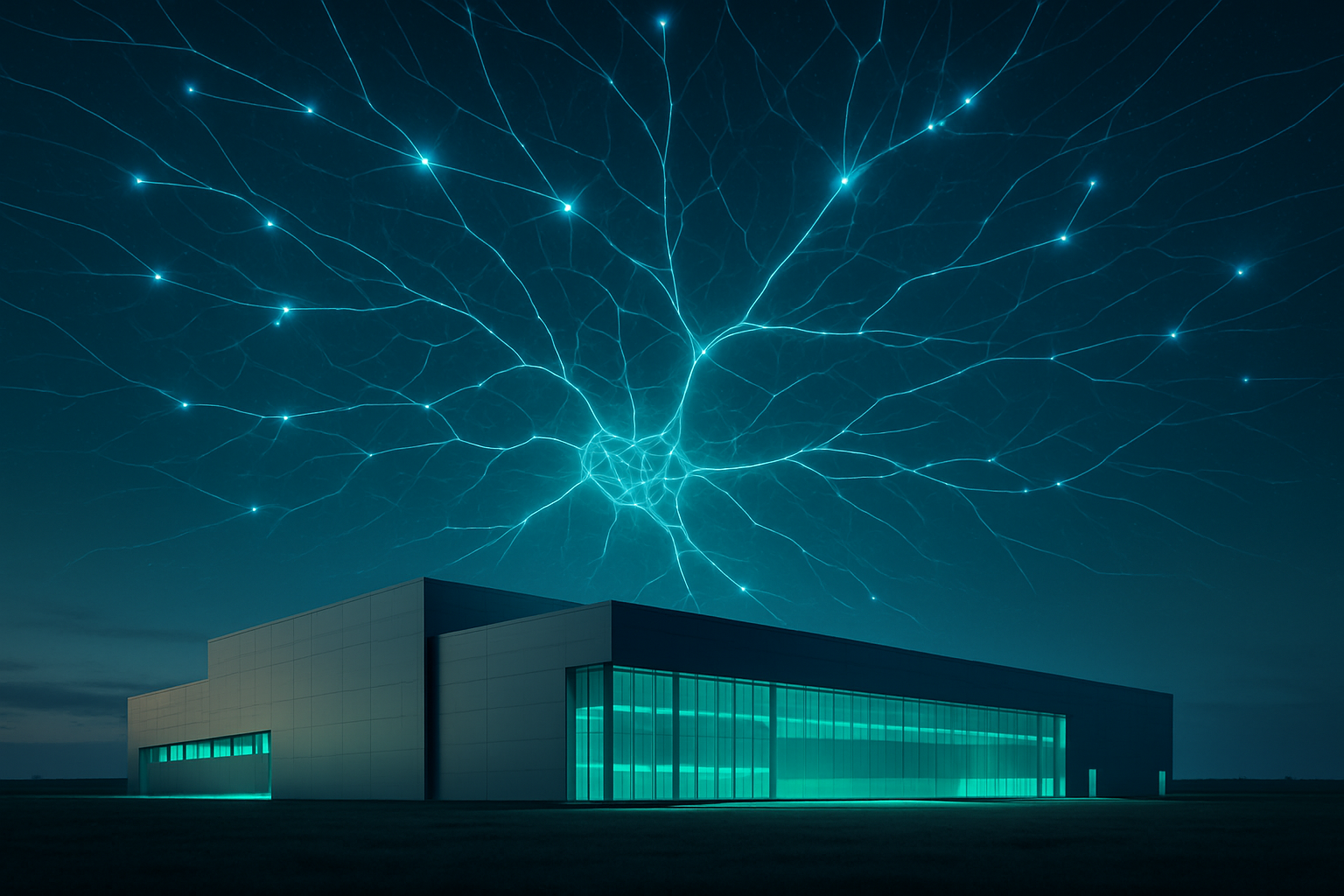
    Engineering the Future: The Technical Marvels Powering AI's Ascent

    The relentless march of progress in AI is intrinsically linked to groundbreaking innovations within semiconductor technology. Recent advancements in chip architecture, materials science, and manufacturing processes are pushing the boundaries of what's possible, fundamentally altering the performance, power efficiency, and cost of the hardware that drives artificial intelligence.

    Gate-All-Around FET (GAAFET) Transistors represent a pivotal evolution in transistor design, succeeding the FinFET architecture. While FinFETs improved electrostatic control by wrapping the gate around three sides of a fin-shaped channel, GAAFETs take this a step further by completely enclosing the channel on all four sides, typically using nanowire or stacked nanosheet technology. This "gate-all-around" design provides unparalleled control over current flow, drastically minimizing leakage and short-channel effects at advanced nodes (e.g., 3nm and beyond). Companies like Samsung (KRX: 005930) with its MBCFET and Intel (NASDAQ: INTC) with its RibbonFET are leading this transition, promising up to 45% less power consumption and a 16% smaller footprint compared to previous FinFET processes, crucial for denser, more energy-efficient AI processors.

    3D Stacking (3D ICs) is revolutionizing chip design by moving beyond traditional 2D layouts. Instead of placing components side-by-side, 3D stacking involves vertically integrating multiple semiconductor dies (chips) and interconnecting them with Through-Silicon Vias (TSVs). This "high-rise" approach dramatically increases compute density, allowing for significantly more processing power within the same physical footprint. Crucially for AI, it shortens interconnect lengths, leading to ultra-fast data transfer, significantly higher memory bandwidth, and reduced latency—addressing the notorious "memory wall" problem. AI accelerators utilizing 3D stacking have demonstrated up to a 50% improvement in performance per watt and can deliver up to 10 times faster AI inference and training, making it indispensable for data centers and edge AI.

    Wide-Bandgap (WBG) Materials like Silicon Carbide (SiC) and Gallium Nitride (GaN) are transforming power electronics, a critical but often overlooked component of AI infrastructure. Unlike traditional silicon, these materials boast superior electrical and thermal properties, including wider bandgaps and higher breakdown electric fields. SiC, with its ability to withstand higher voltages and temperatures, is ideal for high-power applications, significantly reducing switching losses and enabling more efficient power conversion in AI data centers and electric vehicles. GaN, excelling in high-frequency operations and offering superior electron mobility, allows for even faster switching speeds and greater power density, making power supplies for AI servers smaller, lighter, and more efficient. Their deployment directly reduces the energy footprint of AI, which is becoming a major concern.

    Extreme Ultraviolet (EUV) Lithography is the linchpin enabling the fabrication of these advanced chips. By utilizing an extremely short wavelength of 13.5 nm, EUV allows manufacturers to print incredibly fine patterns on silicon wafers, creating features well below 10 nm. This capability is absolutely essential for manufacturing 7nm, 5nm, 3nm, and upcoming 2nm process nodes, which are the foundation for packing billions of transistors onto a single chip. Without EUV, the semiconductor industry would have hit a physical wall in its quest for continuous miniaturization, directly impeding the exponential growth trajectory of AI's computational capabilities. Leading foundries like Taiwan Semiconductor Manufacturing Company (TSMC) (NYSE: TSM), Samsung (KRX: 005930), and Intel (NASDAQ: INTC) have heavily invested in EUV, recognizing its critical role in sustaining Moore's Law and delivering the raw processing power demanded by sophisticated AI models.

    Initial reactions from the AI research community and industry experts are overwhelmingly positive, viewing these innovations as "foundational to the continued advancement of artificial intelligence." Experts emphasize that these technologies are not just making existing AI faster but are enabling entirely new paradigms, such as more energy-efficient neuromorphic computing and advanced edge AI, by providing the necessary hardware muscle.

    Reshaping the Tech Landscape: Competitive Dynamics and Market Positioning

    The relentless pace of semiconductor innovation is profoundly reshaping the competitive dynamics across the technology industry, creating both immense opportunities and significant challenges for AI companies, tech giants, and startups alike.

    NVIDIA (NASDAQ: NVDA), a dominant force in AI GPUs, stands to benefit immensely. Their market leadership in AI accelerators is directly tied to their ability to leverage cutting-edge foundry processes and advanced packaging. The superior performance and energy efficiency enabled by EUV-fabricated chips and 3D stacking directly translate into more powerful and desirable AI solutions, further solidifying NVIDIA's competitive edge and strengthening its CUDA software platform. The company is actively integrating wide-bandgap materials like GaN and SiC into its data center architectures for improved power management.

    Intel (NASDAQ: INTC) and Advanced Micro Devices (NASDAQ: AMD) are aggressively pursuing their own strategies. Intel's "IDM 2.0" strategy, focusing on manufacturing leadership, sees it investing heavily in GAAFET (RibbonFET) and advanced packaging (Foveros, EMIB) for its upcoming process nodes (Intel 18A, 14A). This is a direct play to regain market share in the high-performance computing and AI segments. AMD, a fabless semiconductor company, relies on partners like TSMC (NYSE: TSM) for advanced manufacturing. Its EPYC processors with 3D V-Cache and MI300 series AI accelerators demonstrate how it leverages these innovations to deliver competitive performance in AI and data center markets.

    Cloud Providers like Amazon (NASDAQ: AMZN) (AWS), Alphabet (NASDAQ: GOOGL) (Google), and Microsoft (NASDAQ: MSFT) are increasingly becoming custom silicon powerhouses. They are designing their own AI chips (e.g., AWS Trainium and Inferentia, Google TPUs, Microsoft Azure Maia) to optimize performance, power efficiency, and cost for their vast data centers and AI services. This vertical integration allows them to tailor hardware precisely to their AI workloads, reducing reliance on external suppliers and gaining a strategic advantage in the fiercely competitive cloud AI market. The adoption of SiC and GaN in their data center power delivery systems is also critical for managing the escalating energy demands of AI.

    For semiconductor foundries like TSMC (NYSE: TSM) and Samsung (KRX: 005930), and increasingly Intel Foundry Services (IFS), the race for process leadership at 3nm, 2nm, and beyond, coupled with advanced packaging capabilities, is paramount. Their ability to deliver GAAFET-based chips and sophisticated 3D stacking solutions is what attracts the top-tier AI chip designers. Samsung's "one-stop shop" approach, integrating memory, foundry, and packaging, aims to streamline AI chip production.

    Startups in the AI hardware space face both immense opportunities and significant barriers. While they can leverage these cutting-edge technologies to develop highly specialized and energy-efficient AI hardware, access to advanced fabrication capabilities, with their immense complexity and exorbitant costs, remains a major hurdle. Strategic partnerships with leading foundries and design houses are crucial for these smaller players to bring their innovations to market.

    The competitive implications are clear: companies that successfully integrate and leverage these semiconductor advancements into their products and services—whether as chip designers, manufacturers, or end-users—are best positioned to thrive in the evolving AI landscape. This also signals a potential disruption to traditional monolithic chip designs, with a growing emphasis on modular chiplet architectures and advanced packaging to maximize performance and efficiency.

    A New Era of Intelligence: Wider Significance and Emerging Concerns

    The profound advancements in semiconductor technology extend far beyond the direct realm of AI hardware, reshaping industries, economies, and societies on a global scale. These innovations are not merely making existing technologies faster; they are enabling entirely new capabilities and paradigms that will define the next generation of intelligent systems.

    In the automotive industry, SiC and GaN are pivotal for the ongoing electric vehicle (EV) revolution. SiC power electronics are extending EV range, improving charging speeds, and enabling the transition to more efficient 800V architectures. GaN's high-frequency capabilities are enhancing on-board chargers and power inverters, making them smaller and lighter. Furthermore, 3D stacked memory integrated with AI processors is critical for advanced driver-assistance systems (ADAS) and autonomous driving, allowing vehicles to process vast amounts of sensor data in real-time for safer and more reliable operation.

    Data centers, the backbone of the AI economy, are undergoing a massive transformation. GAAFETs contribute to lower power consumption, while 3D stacking significantly boosts compute density (up to five times more processing power in the same footprint) and improves thermal management, with chips dissipating heat up to three times more effectively. GaN semiconductors in server power supplies can cut energy use by 10%, creating more space for AI accelerators. These efficiencies are crucial as AI workloads drive an unprecedented surge in energy demand, making sustainable data center operations a paramount concern.

    The telecommunications sector is also heavily reliant on these innovations. GaN's high-frequency performance and power handling are essential for the widespread deployment of 5G and the development of future 6G networks, enabling faster, more reliable communication and advanced radar systems. In consumer electronics, GAAFETs enable more powerful and energy-efficient mobile processors, translating to longer battery life and faster performance in smartphones and other devices, while GaN has already revolutionized compact and rapid charging solutions.

    The economic implications are staggering. The global semiconductor industry, currently valued around $600 billion, is projected to surpass $1 trillion by the end of the decade, largely fueled by AI. The AI chip market alone is expected to exceed $150 billion in 2025 and potentially reach over $400 billion by 2027. This growth fuels innovation, creates new markets, and boosts operational efficiency across countless industries.

    However, this rapid progress comes with emerging concerns. The geopolitical competition for dominance in advanced chip technology has intensified, with nations recognizing semiconductors as strategic assets critical for national security and economic leadership. The "chip war" highlights the vulnerabilities of a highly concentrated and interdependent global supply chain, particularly given that a single region (Taiwan) produces a vast majority of the world's most advanced semiconductors.

    Environmental impact is another critical concern. Semiconductor manufacturing is incredibly resource-intensive, consuming vast amounts of water, energy, and hazardous chemicals. EUV tools, in particular, are extremely energy-hungry, with a single machine rivaling the annual energy consumption of an entire city. Addressing these environmental footprints through energy-efficient production, renewable energy adoption, and advanced waste management is crucial for sustainable growth.

    Furthermore, the exorbitant costs associated with developing and implementing these advanced technologies (a new sub-3nm fabrication plant can cost up to $20 billion) create high barriers to entry, concentrating innovation and manufacturing capabilities among a few dominant players. This raises concerns about accessibility and could potentially widen the digital divide, limiting broader participation in the AI revolution.

    In terms of AI history, these semiconductor developments represent a watershed moment. They have not merely facilitated the growth of AI but have actively shaped its trajectory, pushing it from theoretical potential to ubiquitous reality. The current "AI Supercycle" is a testament to this symbiotic relationship, where the insatiable demands of AI for computational power drive semiconductor innovation, and in turn, advanced silicon unlocks new AI capabilities, creating a self-reinforcing loop of progress. This is a period of foundational hardware advancements, akin to the invention of the transistor or the advent of the GPU, that physically enables the execution of sophisticated AI models and opens doors to entirely new paradigms like neuromorphic and quantum-enhanced computing.

    The Horizon of Intelligence: Future Developments and Challenges

    The future of AI is inextricably linked to the trajectory of semiconductor innovation. The coming years promise a fascinating array of developments that will push the boundaries of computational power, efficiency, and intelligence, albeit alongside significant challenges.

    In the near-term (1-5 years), the industry will see a continued focus on refining existing silicon-based technologies. This includes the mainstream adoption of 3nm and 2nm process nodes, enabling even higher transistor density and more powerful AI chips. Specialized AI accelerators (ASICs, NPUs) will proliferate further, with tech giants heavily investing in custom silicon tailored for their specific cloud AI workloads. Heterogeneous integration and advanced packaging, particularly chiplets and 3D stacking with High-Bandwidth Memory (HBM), will become standard for high-performance computing (HPC) and AI, crucial for overcoming memory bottlenecks and maximizing computational throughput. Silicon photonics is also poised to emerge as a critical technology for addressing data movement bottlenecks in AI data centers, enabling faster and more energy-efficient data transfer.

    Looking long-term (beyond 5 years), more radical shifts are on the horizon. Neuromorphic computing, inspired by the human brain, aims to achieve drastically lower energy consumption for AI tasks by utilizing spiking neural networks (SNNs). Companies like Intel (NASDAQ: INTC) with Loihi and IBM (NYSE: IBM) with TrueNorth are exploring this path, with potential energy efficiency improvements of up to 1000x for specific AI inference tasks. These systems could revolutionize edge AI and robotics, enabling highly adaptable, real-time processing with minimal power.

    Further advancements in transistor architectures, such as Complementary FETs (CFETs), which vertically stack n-type and p-type GAAFETs, promise even greater density and efficiency. Research into beyond-silicon materials, including chalcogenides and 2D materials, will be crucial for overcoming silicon's physical limitations in performance, power efficiency, and heat resistance, especially for high-performance and heat-resistant applications. The eventual integration with quantum computing could unlock unprecedented computational capabilities for AI, leveraging quantum superposition and entanglement to solve problems currently intractable for classical computers, though this remains a more distant prospect.

    These future developments will enable a plethora of potential applications. Neuromorphic computing will empower more sophisticated robotics, real-time healthcare diagnostics, and highly efficient edge AI for IoT devices. Quantum-enhanced AI could revolutionize drug discovery, materials science, and natural language processing by tackling complex problems at an atomic level. Advanced edge AI will be critical for truly autonomous systems, smart cities, and personalized electronics, enabling real-time decision-making without reliance on cloud connectivity.

    Crucially, AI itself is transforming chip design. AI-driven Electronic Design Automation (EDA) tools are already automating complex tasks like schematic generation and layout optimization, significantly reducing design cycles from months to weeks and optimizing performance, power, and area (PPA) with extreme precision. AI will also play a vital role in manufacturing optimization, predictive maintenance, and supply chain management within the semiconductor industry.

    However, significant challenges need to be addressed. The escalating power consumption and heat management of AI workloads demand massive upgrades in data center infrastructure, including new liquid cooling systems, as traditional air cooling becomes insufficient. The development of advanced materials beyond silicon faces hurdles in growth quality, material compatibility, and scalability. The manufacturing costs of advanced process nodes continue to soar, creating financial barriers and intensifying the need for economies of scale. Finally, a critical global talent shortage in the semiconductor industry, particularly for engineers and process technologists, threatens to impede progress, requiring strategic investments in workforce training and development.

    Experts predict that the "AI supercycle" will continue to drive unprecedented investment and innovation in the semiconductor industry, creating a profound and mutually beneficial partnership. The demand for specialized AI chips will skyrocket, fueling R&D and capital expansion. The race for superior HBM and other high-performance memory solutions will intensify, as will the competition for advanced packaging and process leadership.

    The Unfolding Symphony: A Comprehensive Wrap-up

    The fundamental contribution of the semiconductor industry to broader technological advancements, particularly in AI, cannot be overstated. From the intricate logic of Gate-All-Around FETs to the high-density integration of 3D stacking, the energy efficiency of SiC and GaN, and the precision of EUV lithography, these innovations form the very foundation upon which the modern digital world and the burgeoning AI era are built. They are the silent, yet powerful, enablers of every smart device, every cloud service, and every AI-driven breakthrough.

    In the annals of AI history, these semiconductor developments represent a watershed moment. They have not merely facilitated the growth of AI but have actively shaped its trajectory, pushing it from theoretical potential to ubiquitous reality. The current "AI Supercycle" is a testament to this symbiotic relationship, where the insatiable demands of AI for computational power drive semiconductor innovation, and in turn, advanced silicon unlocks new AI capabilities, creating a self-reinforcing loop of progress. This is a period of foundational hardware advancements, akin to the invention of the transistor or the advent of the GPU, that physically enables the execution of sophisticated AI models and opens doors to entirely new paradigms like neuromorphic and quantum-enhanced computing.

    The long-term impact on technology and society will be profound and transformative. We are moving towards a future where AI is deeply embedded across all industries and aspects of daily life, from fully autonomous vehicles and smart cities to personalized medicine and intelligent robotics. These semiconductor innovations will make AI systems more efficient, accessible, and cost-effective, democratizing access to advanced intelligence and driving unprecedented breakthroughs in scientific research and societal well-being. However, this progress is not without its challenges, including the escalating costs of development, geopolitical tensions over supply chains, and the environmental footprint of manufacturing, all of which demand careful global management and responsible innovation.

    In the coming weeks and months, several key trends warrant close observation. Watch for continued announcements regarding manufacturing capacity expansions from leading foundries, particularly the progress of 2nm process volume production expected in late 2025. The competitive landscape for AI chips will intensify, with new architectures and product lines from AMD (NASDAQ: AMD) and Intel (NASDAQ: INTC) challenging NVIDIA's (NASDAQ: NVDA) dominance. The performance and market traction of "AI-enabled PCs," integrating AI directly into operating systems, will be a significant indicator of mainstream AI adoption. Furthermore, keep an eye on advancements in 3D chip stacking, novel packaging techniques, and the exploration of non-silicon materials, as these will be crucial for pushing beyond current limitations. Developments in neuromorphic computing and silicon photonics, along with the increasing trend of in-house chip development by major tech giants, will signal the diversification and specialization of the AI hardware ecosystem. Finally, the ongoing geopolitical dynamics and efforts to build resilient supply chains will remain critical factors shaping the future of this indispensable industry.

    This content is intended for informational purposes only and represents analysis of current AI developments.

    TokenRing AI delivers enterprise-grade solutions for multi-agent AI workflow orchestration, AI-powered development tools, and seamless remote collaboration platforms.
    For more information, visit https://www.tokenring.ai/.

  • AI’s Silicon Revolution: How Intelligent Machines are Redrawing the Semiconductor Landscape

    AI’s Silicon Revolution: How Intelligent Machines are Redrawing the Semiconductor Landscape

    The Artificial Intelligence (AI) revolution is not merely consuming advanced technology; it is actively reshaping the very foundations of its existence – the semiconductor industry. From dictating unprecedented demand for cutting-edge chips to fundamentally transforming their design and manufacturing, AI has become the primary catalyst driving a profound and irreversible shift in silicon innovation. This symbiotic relationship, where AI fuels the need for more powerful hardware and simultaneously becomes the architect of its creation, is ushering in a new era of technological advancement, creating immense market opportunities, and redefining global tech leadership.

    The insatiable computational appetite of modern AI, particularly for complex models like generative AI and large language models (LLMs), has ignited an unprecedented demand for high-performance semiconductors. This surge is not just about more chips, but about chips that are exponentially faster, more energy-efficient, and highly specialized. This dynamic is propelling the semiconductor industry into an accelerated cycle of innovation, making it the bedrock of the global AI economy and positioning it at the forefront of the next technological frontier.

    The Technical Crucible: AI Forging the Future of Silicon

    AI's technical influence on semiconductors spans the entire lifecycle, from conception to fabrication, leading to groundbreaking advancements in design methodologies, novel architectures, and packaging technologies. This represents a significant departure from traditional, often manual, or rule-based approaches.

    At the forefront of this transformation are AI-driven Electronic Design Automation (EDA) tools. These sophisticated platforms leverage machine learning and deep learning algorithms, including reinforcement learning and generative AI, to automate and optimize intricate chip design processes. Companies like Synopsys (NASDAQ: SNPS) and Cadence Design Systems (NASDAQ: CDNS) are pioneering these tools, which can explore billions of design configurations for optimal Power, Performance, and Area (PPA) at speeds far beyond human capability. Synopsys's DSO.ai, for instance, has reportedly slashed the design optimization cycle for a 5nm chip from six months to a mere six weeks, a 75% reduction in time-to-market. These AI systems automate tasks such as logic synthesis, floor planning, routing, and timing analysis, while also predicting potential flaws and enhancing verification robustness, drastically improving design efficiency and quality compared to previous iterative, human-intensive methods.

    Beyond conventional designs, AI is catalyzing the emergence of neuromorphic computing. This radical architecture, inspired by the human brain, integrates memory and processing directly on the chip, eliminating the "Von Neumann bottleneck" inherent in traditional computers. Neuromorphic chips, like Intel's (NASDAQ: INTC) Loihi series and its large-scale Hala Point system (featuring 1.15 billion neurons), operate on an event-driven model, consuming power only when neurons are active. This leads to exceptional energy efficiency and real-time adaptability, making them ideal for tasks like pattern recognition and sensory data processing—a stark contrast to the energy-intensive, sequential processing of conventional AI systems.

    Furthermore, advanced packaging technologies are becoming indispensable, with AI playing a crucial role in their innovation. As traditional Moore's Law scaling faces physical limits, integrating multiple semiconductor components (chiplets) into a single package through 2.5D and 3D stacking has become critical. Technologies like TSMC's (NYSE: TSM) CoWoS (Chip-on-Wafer-on-Substrate) allow for the vertical integration of memory (e.g., High-Bandwidth Memory – HBM) and logic chips. This close integration dramatically reduces data travel distance, boosting bandwidth and reducing latency, which is vital for high-performance AI chips. For example, NVIDIA's (NASDAQ: NVDA) H100 AI chip uses CoWoS to achieve 4.8 TB/s interconnection speeds. AI algorithms optimize packaging design, improve material selection, automate quality control, and predict defects, making these complex multi-chip integrations feasible and efficient.

    The AI research community and industry experts have universally hailed AI's role as a "game-changer" and "critical enabler" for the next wave of innovation. Many suggest that AI chip development is now outpacing traditional Moore's Law, with AI's computational power doubling approximately every six months. Experts emphasize that AI-driven EDA tools free engineers from mundane tasks, allowing them to focus on architectural breakthroughs, thereby addressing the escalating complexity of modern chip designs and the growing talent gap in the semiconductor industry. This symbiotic relationship is creating a self-reinforcing cycle of innovation that promises to push technological boundaries further and faster.

    Corporate Chessboard: Beneficiaries, Battles, and Strategic Shifts

    The AI-driven semiconductor revolution is redrawing the competitive landscape, creating clear winners, intense rivalries, and strategic shifts among tech giants and startups alike.

    NVIDIA (NASDAQ: NVDA) remains the undisputed leader in the AI chip market. Its Graphics Processing Units (GPUs), such as the A100 and H100, coupled with its robust CUDA software platform, have become the de facto standard for AI training and inference. This powerful hardware-software ecosystem creates significant switching costs for customers, solidifying NVIDIA's competitive moat. The company's data center business has experienced exponential growth, with AI sales forming a substantial portion of its revenue. Upcoming Blackwell AI chips, including the GeForce RTX 50 Series, are expected to further cement its market dominance.

    Challengers are emerging, however. AMD (NASDAQ: AMD) is rapidly gaining ground with its Instinct MI series GPUs and EPYC CPUs. A multi-year, multi-billion dollar agreement to supply AI chips to OpenAI, including the deployment of MI450 systems, marks a significant win for AMD, positioning it as a crucial player in the global AI supply chain. This partnership, which also includes OpenAI acquiring up to a 10% equity stake in AMD, validates the performance of AMD's Instinct GPUs for demanding AI workloads. Intel (NASDAQ: INTC), while facing stiff competition, is also actively pursuing its AI chip strategy, developing AI accelerators and leveraging its CPU technology, alongside investments in foundry services and advanced packaging.

    At the manufacturing core, TSMC (NYSE: TSM) is an indispensable titan. As the world's largest contract chipmaker, it fabricates nearly all of the most advanced chips for NVIDIA, AMD, Google, and Amazon. TSMC's cutting-edge process technologies (e.g., 3nm, 5nm) and advanced packaging solutions like CoWoS are critical enablers for high-performance AI chips. The company is aggressively expanding its CoWoS production capacity to meet surging AI chip demand, with AI-related applications significantly boosting its revenue. Similarly, ASML (NASDAQ: ASML) holds a near-monopoly in Extreme Ultraviolet (EUV) lithography machines, essential for manufacturing these advanced chips. Without ASML's technology, the production of next-generation AI silicon would be impossible, granting it a formidable competitive moat and pricing power.

    A significant competitive trend is the vertical integration by tech giants. Companies like Google (NASDAQ: GOOGL) with its Tensor Processing Units (TPUs), Amazon (NASDAQ: AMZN) with Trainium and Inferentia for AWS, and Microsoft (NASDAQ: MSFT) with its Azure Maia AI Accelerator and Cobalt CPU, are designing their own custom AI silicon. This strategy aims to optimize hardware precisely for their specific AI models and workloads, reduce reliance on external suppliers (like NVIDIA), lower costs, and enhance control over their cloud infrastructure. Meta Platforms (NASDAQ: META) is also aggressively pursuing custom AI chips, unveiling its second-generation Meta Training and Inference Accelerator (MTIA) and acquiring chip startup Rivos to bolster its in-house silicon development, driven by its expansive AI ambitions for generative AI and the metaverse.

    For startups, the landscape presents both opportunities and challenges. Niche innovators can thrive by developing highly specialized AI accelerators or innovative software tools for AI chip design. However, they face significant hurdles in securing capital-intensive funding and competing with the massive R&D budgets of tech giants. Some startups may become attractive acquisition targets, as evidenced by Meta's acquisition of Rivos. The increasing capacity in advanced packaging, however, could democratize access to critical technologies, fostering innovation from smaller players. The overall economic impact is staggering, with the AI chip market alone projected to surpass $150 billion in 2025 and potentially exceed $400 billion by 2027, signaling an immense financial stake and driving a "supercycle" of investment and innovation.

    Broader Horizons: Societal Shifts and Geopolitical Fault Lines

    The profound impact of AI on the semiconductor industry extends far beyond corporate balance sheets, touching upon wider societal implications, economic shifts, and geopolitical tensions. This dynamic fits squarely into the broader AI landscape, where hardware advancements are fundamental to unlocking increasingly sophisticated AI capabilities.

    Economically, the AI-driven semiconductor surge is generating unprecedented market growth. The global semiconductor market is projected to reach $1 trillion by 2030, with generative AI potentially pushing it to $1.3 trillion. The AI chip market alone is a significant contributor, with projections of hundreds of billions in sales within the next few years. This growth is attracting massive investment in capital expenditures, particularly for advanced manufacturing nodes and strategic partnerships, concentrating economic profit among a select group of top-tier companies. While automation in chip design and manufacturing may lead to some job displacement in traditional roles, it simultaneously creates demand for a new workforce skilled in AI and data science, necessitating extensive reskilling initiatives.

    However, this transformative period is not without its concerns. The supply chain for AI chips faces rising risks due to extreme geographic concentration. Over 90% of the world's most advanced chips (<10nm) are manufactured by TSMC in Taiwan and Samsung in South Korea, while the US leads in chip design and manufacturing equipment. This high concentration creates significant vulnerabilities to geopolitical disruptions, natural disasters, and reliance on single-source equipment providers like ASML for EUV lithography. To mitigate these risks, companies are shifting from "just-in-time" to "just-in-case" inventory models, stockpiling critical components.

    The immense energy consumption of AI is another growing concern. The computational demands of training and running large AI models lead to a substantial increase in electricity usage. Global data center electricity consumption is projected to double by 2030, with AI being the primary driver, potentially accounting for nearly half of data center power consumption by the end of 2025. This surge in energy, often from fossil fuels, contributes to greenhouse gas emissions and increased water usage for cooling, raising environmental and economic sustainability questions.

    Geopolitical implications are perhaps the most significant wider concern. The "AI Cold War," primarily between the United States and China, has elevated semiconductors to strategic national assets, leading to a "Silicon Curtain." Nations are prioritizing technological sovereignty over economic efficiency, resulting in export controls (e.g., US restrictions on advanced AI chips to China), trade wars, and massive investments in domestic semiconductor production (e.g., US CHIPS Act, European Chips Act). This competition risks creating bifurcated technological ecosystems with parallel supply chains and potentially divergent standards, impacting global innovation and interoperability. While the US aims to maintain its competitive advantage, China is aggressively pursuing self-sufficiency in advanced AI chip production, though a significant performance gap remains in complex analytics and advanced manufacturing.

    Comparing this to previous AI milestones, the current surge is distinct. While early AI relied on mainframes and the GPU revolution (1990s-2010s) accelerated deep learning, the current era is defined by purpose-built AI accelerators and the integration of AI into the chip design process itself. This marks a transition where AI is not just enabled by hardware, but actively shaping its evolution, pushing beyond the traditional limits of Moore's Law through advanced packaging and novel architectures.

    The Horizon Beckons: Future Trajectories and Emerging Frontiers

    The future trajectory of AI's impact on the semiconductor industry promises continued, rapid innovation, driven by both evolutionary enhancements and revolutionary breakthroughs. Experts predict a robust and sustained era of growth, with the semiconductor market potentially reaching $1 trillion by 2030, largely fueled by AI.

    In the near-term (1-3 years), expect further advancements in AI-driven EDA tools, leading to even greater automation in chip design, verification, and intellectual property (IP) discovery. Generative AI is poised to become a "game-changer," enabling more complex designs and freeing engineers to focus on higher-level architectural innovations, significantly reducing time-to-market. In manufacturing, AI will drive self-optimizing systems, including advanced predictive maintenance, highly accurate AI-enhanced image recognition for defect detection, and machine learning models that optimize production parameters for improved yield and efficiency. Real-time quality control and AI-streamlined supply chain management will become standard.

    Longer-term (5-10+ years), we anticipate fully autonomous manufacturing environments, drastically reducing labor costs and human error, and fundamentally reshaping global production strategies. Technologically, AI will drive disruptive hardware architectures, including more sophisticated neuromorphic computing designs and chips specifically optimized for quantum computing workloads. The quest for fault-tolerant quantum computing through robust error correction mechanisms is the ultimate goal in this domain. Highly resilient and secure chips with advanced hardware-level security features will also become commonplace, while AI will facilitate the exploration of new materials with unique properties, opening up entirely new markets for customized semiconductor offerings across diverse sectors.

    Edge AI is a critical and expanding frontier. AI processing is increasingly moving closer to the data source—on-device—reducing latency, conserving bandwidth, enhancing privacy, and enabling real-time decision-making. This will drive demand for specialized, low-power, high-performance semiconductors in autonomous vehicles, industrial automation, augmented reality devices, smart home appliances, robotics, and wearable healthcare monitors. These Edge AI chips prioritize power efficiency, memory usage, and processing speed within tight constraints.

    The proliferation of specialized AI accelerators will continue. While GPUs remain dominant for training, Application-Specific Integrated Circuits (ASICs), Field-Programmable Gate Arrays (FPGAs), and Neural Processing Units (NPUs) are becoming essential for specific AI tasks like deep learning inference, natural language processing, and image recognition, especially at the edge. Custom System-on-Chip (SoC) designs, integrating multiple accelerator types, will become powerful enablers for compact, edge-based AI deployments.

    However, several challenges must be addressed. Energy efficiency and heat dissipation remain paramount, as high-performance AI chips can consume over 500 watts, demanding innovative cooling solutions and architectural optimizations. The cost and scalability of building state-of-the-art fabrication plants (fabs) are immense, creating high barriers to entry. The complexity and precision required for modern AI chip design at atomic scales (e.g., 3nm transistors) necessitate advanced tools and expertise. Data scarcity and quality for training AI models in semiconductor design and manufacturing, along with the interpretability and validation of "black box" AI decisions, pose significant hurdles. Finally, a critical workforce shortage of professionals proficient in both AI algorithms and semiconductor technology (projected to exceed one million additional skilled workers by 2030) and persistent supply chain and geopolitical challenges demand urgent attention.

    Experts predict a continued "arms race" in chip development, with heavy investments in advanced packaging technologies like 3D stacking and chiplets to overcome traditional scaling limitations. AI is expected to become the "backbone of innovation," dramatically accelerating the adoption of AI and machine learning in semiconductor manufacturing. The shift in demand from consumer devices to data centers and cloud infrastructure will continue to fuel the need for High-Performance Computing (HPC) chips and custom silicon. Near-term developments will focus on optimizing AI accelerators for energy efficiency and specialized architectures, while long-term predictions include the emergence of novel computing paradigms like neuromorphic and quantum computing, fundamentally reshaping chip design and AI capabilities.

    The Silicon Supercycle: A Transformative Era

    The profound impact of Artificial Intelligence on the semiconductor industry marks a transformative era, often dubbed the "Silicon Supercycle." The key takeaway is a symbiotic relationship: AI is not merely a consumer of advanced chips but an indispensable architect of their future. This dynamic is driving unprecedented demand for high-performance, specialized silicon, while simultaneously revolutionizing chip design, manufacturing, and packaging through AI-driven tools and methodologies.

    This development is undeniably one of the most significant in AI history, fundamentally accelerating technological progress across the board. It ensures that the physical infrastructure required for increasingly complex AI models can keep pace with algorithmic advancements. The strategic importance of semiconductors has never been higher, intertwining technological leadership with national security and economic power.

    Looking ahead, the long-term impact will be a world increasingly powered by highly optimized, intelligent hardware, enabling AI to permeate every aspect of society, from autonomous systems and advanced healthcare to personalized computing and beyond. The coming weeks and months will see continued announcements of new AI chip designs, further investments in advanced manufacturing capacity, and intensified competition among tech giants and semiconductor firms to secure their position in this rapidly evolving landscape. Watch for breakthroughs in energy-efficient AI hardware, advancements in AI-driven EDA, and continued geopolitical maneuvering around the global semiconductor supply chain. The AI-driven silicon revolution is just beginning, and its ripples will define the technological future.


    This content is intended for informational purposes only and represents analysis of current AI developments.

    TokenRing AI delivers enterprise-grade solutions for multi-agent AI workflow orchestration, AI-powered development tools, and seamless remote collaboration platforms. For more information, visit https://www.tokenring.ai/.

  • Google’s $4 Billion Arkansas Bet: Fueling the Future of U.S. AI Innovation

    Google’s $4 Billion Arkansas Bet: Fueling the Future of U.S. AI Innovation

    Google (NASDAQ: GOOGL) has announced a monumental $4 billion investment in cloud and artificial intelligence (AI) infrastructure in Arkansas through 2027, marking a significant stride in the tech giant's commitment to advancing U.S. AI capabilities. This substantial financial injection will primarily fund the construction of Google's first data center in the state, located in West Memphis, and underscores a strategic push to expand the company's regional cloud presence and enhance its AI processing power. The announcement, made on October 2, 2025, with further elaborations by Google and Alphabet CEO Sundar Pichai on October 6, 2025, highlights Arkansas's emerging role in the national AI landscape.

    This multi-faceted investment is poised to have immediate and far-reaching implications for AI innovation across the United States. By establishing a new, massive data center and integrating sustainable energy solutions, Google is not only scaling its operational capacity but also setting a precedent for responsible AI development. The initiative is expected to generate thousands of jobs, foster a skilled workforce through free AI training programs, and solidify the U.S.'s competitive edge in the global AI race, demonstrating Google's dedication to both technological advancement and regional economic growth.

    The Technical Core of Google's Arkansas Expansion

    Google's $4 billion investment is anchored by the development of its first Arkansas data center, an expansive facility spanning over 1,000 acres in West Memphis. This new infrastructure is meticulously designed to serve as a critical hub for cloud and AI operations, providing the colossal computing power necessary to train sophisticated large language models and process the ever-growing datasets that fuel advanced AI applications. The scale of this data center signifies a substantial increase in Google's capacity to handle the surging demand for AI computing, offering enhanced reliability and speed for businesses relying on AI-powered cloud services, particularly in the Southern U.S.

    Beyond the physical data center, Google is integrating cutting-edge energy initiatives to power its operations sustainably. A $25 million Energy Impact Fund will support energy efficiency and affordability for local residents, while a collaboration with Entergy will bring a new 600 MW solar project to the grid, complemented by a 350 MW battery storage system. This commitment to renewable energy and grid stability differentiates Google's approach, demonstrating an effort to mitigate the significant energy demands typically associated with large-scale AI infrastructure. This sustainable design is a crucial evolution from previous data center models, which often faced criticism for their environmental footprint, positioning Google as a leader in eco-conscious AI development.

    Initial reactions from the AI research community and industry experts have been overwhelmingly positive. Many see this investment as a vital step in strengthening the foundational infrastructure required for the next generation of AI breakthroughs. The emphasis on both raw processing power and sustainable energy has been particularly lauded, indicating a maturing understanding within the industry of the broader societal and environmental responsibilities that come with scaling AI technologies. Experts predict that this robust infrastructure will accelerate research and development in areas like generative AI, advanced machine learning, and autonomous systems.

    Competitive Implications and Market Positioning

    This significant investment by Google (NASDAQ: GOOGL) in Arkansas carries profound implications for the competitive landscape of the AI sector, impacting tech giants, emerging AI labs, and startups alike. Google's expansion of its cloud and AI infrastructure directly strengthens its competitive position against rivals such as Amazon (NASDAQ: AMZN) with Amazon Web Services (AWS) and Microsoft (NASDAQ: MSFT) with Azure, both of whom are also heavily investing in AI-driven cloud solutions. By increasing its data center footprint and processing capabilities, Google can offer more robust, faster, and potentially more cost-effective AI services, attracting a broader array of enterprise clients and developers.

    Companies heavily reliant on Google Cloud for their AI workloads stand to benefit immensely from this development. Startups and mid-sized businesses leveraging Google's AI Platform or various AI/ML APIs will experience enhanced performance, reduced latency, and greater scalability, which are critical for deploying and iterating on AI-powered products and services. This investment could also encourage new startups to build on Google Cloud, given the enhanced infrastructure and the company's commitment to fostering a skilled workforce through its training programs.

    The strategic advantage for Google lies in its ability to further integrate its AI research directly into its cloud offerings. This tight coupling allows for faster deployment of new AI models and features, potentially disrupting existing products or services offered by competitors who may not have the same level of integrated hardware and software development. Furthermore, the focus on sustainable energy solutions could become a key differentiator, appealing to environmentally conscious businesses and governmental organizations. This move solidifies Google's market positioning as not just a leader in AI research, but also as a provider of the foundational infrastructure essential for the widespread adoption and development of AI.

    Broader Significance in the AI Landscape

    Google's $4 billion investment in Arkansas is a pivotal development that seamlessly integrates into the broader AI landscape and reflects several overarching trends. Firstly, it underscores the escalating demand for computational power driven by the rapid advancements in AI, particularly in large language models and complex machine learning algorithms. This investment signifies that the "AI race" is not just about algorithmic innovation, but also about the physical infrastructure required to support it. It aligns with a global trend of major tech players establishing regional data centers to bring AI closer to users and developers, thereby reducing latency and improving service delivery.

    The impacts of this investment extend beyond mere technological expansion. Economically, it promises to revitalize the local Arkansas economy, creating thousands of construction jobs and hundreds of high-skilled operational roles. The provision of free AI courses and certifications, in partnership with the Arkansas Department of Commerce, is a critical initiative aimed at upskilling the local workforce, creating a talent pipeline that will support not only Google's operations but also foster a broader tech ecosystem in the region. This human capital development is crucial for ensuring equitable access to the opportunities presented by the AI revolution.

    While the benefits are substantial, potential concerns could include the environmental impact of such a large-scale data center, even with Google's commitment to renewable energy. The sheer volume of resources required for construction and ongoing operation necessitates careful monitoring. Comparisons to previous AI milestones, such as the initial breakthroughs in deep learning or the widespread adoption of cloud computing, highlight that infrastructure investments of this magnitude are often precursors to significant leaps in technological capability and accessibility. This move by Google is reminiscent of the foundational investments made during the early days of the internet, laying the groundwork for future innovation.

    Future Developments and Expert Predictions

    Looking ahead, Google's substantial investment in Arkansas is expected to catalyze a wave of near-term and long-term developments in the U.S. AI landscape. In the near term, we can anticipate a rapid acceleration in the construction phase of the West Memphis data center, leading to the creation of thousands of construction jobs and a significant boost to local economies. Once operational, the data center will provide a powerful new hub for Google Cloud services, attracting businesses and developers seeking high-performance AI and cloud computing resources, particularly in the Southern U.S.

    In the long term, this infrastructure is poised to unlock a plethora of potential applications and use cases. Enhanced processing power and reduced latency will facilitate the development and deployment of more sophisticated AI models, including advanced generative AI, real-time analytics, and highly complex simulations across various industries. We can expect to see advancements in areas such as precision agriculture, logistics optimization, and personalized healthcare, all powered by the increased AI capabilities. The workforce development initiatives, offering free AI courses and certifications, will also contribute to a more AI-literate population, potentially fostering a new generation of AI innovators and entrepreneurs in Arkansas and beyond.

    However, challenges remain. The continuous demand for energy to power such large-scale AI infrastructure will necessitate ongoing innovation in renewable energy and energy efficiency. Cybersecurity will also be paramount, as these data centers become critical national assets. Experts predict that this investment will solidify Google's position as a dominant player in the AI infrastructure space, potentially leading to further regional investments by other tech giants as they seek to compete. The expectation is that this will foster a more distributed and resilient AI infrastructure across the U.S., ultimately accelerating the pace of AI innovation and its integration into daily life.

    A New Era for U.S. AI Infrastructure

    Google's (NASDAQ: GOOGL) $4 billion investment in Arkansas represents a pivotal moment in the ongoing evolution of artificial intelligence and cloud computing infrastructure in the United States. The construction of a new, state-of-the-art data center in West Memphis, coupled with significant commitments to sustainable energy and workforce development, underscores a strategic vision that extends beyond mere technological expansion. Key takeaways include the substantial boost to U.S. AI processing capabilities, the creation of thousands of jobs, and the establishment of a new regional hub for AI innovation, particularly in the Southern U.S.

    This development holds immense significance in AI history, marking a new chapter where the physical infrastructure supporting AI becomes as critical as the algorithmic breakthroughs themselves. It signifies a move towards a more robust, distributed, and sustainable AI ecosystem, addressing the growing demands for computational power while also acknowledging environmental responsibilities. The investment in human capital through free AI training programs is equally important, ensuring that the benefits of this technological advancement are accessible to a broader segment of the population.

    In the coming weeks and months, industry observers will be closely watching the progress of the data center's construction and the impact of Google's workforce development initiatives. We can expect further announcements regarding partnerships, new AI services leveraging this enhanced infrastructure, and potentially, similar investments from competing tech giants. This monumental undertaking by Google is not just an investment in technology; it is an investment in the future of U.S. AI leadership and a testament to the transformative power of artificial intelligence.

    This content is intended for informational purposes only and represents analysis of current AI developments.

    TokenRing AI delivers enterprise-grade solutions for multi-agent AI workflow orchestration, AI-powered development tools, and seamless remote collaboration platforms.
    For more information, visit https://www.tokenring.ai/.

  • Semiconductor Showdown: Reed Semiconductor and Monolithic Power Systems Clash in High-Stakes IP Battle

    Semiconductor Showdown: Reed Semiconductor and Monolithic Power Systems Clash in High-Stakes IP Battle

    The fiercely competitive semiconductor industry, the bedrock of modern technology, is once again embroiled in a series of high-stakes legal battles, underscoring the critical role of intellectual property (IP) in shaping innovation and market dominance. As of late 2025, a multi-front legal conflict is actively unfolding between Reed Semiconductor Corp., a Rhode Island-based innovator founded in 2019, and Monolithic Power Systems, Inc. (NASDAQ: MPWR), a well-established fabless manufacturer of high-performance power management solutions. This ongoing litigation highlights the intense pressures faced by both emerging players and market leaders in protecting their technological advancements within the vital power management sector.

    This complex legal entanglement sees both companies asserting claims of patent infringement against each other, along with allegations of competitive misconduct. Reed Semiconductor has accused Monolithic Power Systems of infringing its U.S. Patent No. 7,960,955, related to power semiconductor devices incorporating a linear regulator. Conversely, Monolithic Power Systems has initiated multiple lawsuits against Reed Semiconductor and its affiliates, alleging infringement of its own patents concerning power management technologies, including those related to "bootstrap refresh threshold" and "pseudo constant on time control circuit." These cases, unfolding in the U.S. District Courts for the Western District of Texas and the District of Delaware, as well as before the Patent Trial and Appeal Board (PTAB), are not just isolated disputes but a vivid case study into how legal challenges are increasingly defining the trajectory of technological development and market dynamics in the semiconductor industry.

    The Technical Crucible: Unpacking the Patents at the Heart of the Dispute

    At the core of the Reed Semiconductor vs. Monolithic Power Systems litigation lies a clash over fundamental power management technologies crucial for the efficiency and reliability of modern electronic systems. Reed Semiconductor's asserted U.S. Patent No. 7,960,955 focuses on power semiconductor devices that integrate a linear regulator to stabilize input voltage. This innovation aims to provide a consistent and clean internal power supply for critical control circuitry within power management ICs, improving reliability and performance by buffering against input voltage fluctuations. Compared to simpler internal biasing schemes, this integrated linear regulation offers superior noise rejection and regulation accuracy, particularly beneficial in noisy environments or applications demanding precise internal voltage stability. It represents a step towards more robust and precise power management solutions, simplifying overall power conversion design.

    Monolithic Power Systems, in its counter-assertions, has brought forth patents related to "bootstrap refresh threshold" and "pseudo constant on time control circuit." U.S. Patent No. 9,590,608, concerning "bootstrap refresh threshold," describes a control circuit vital for high-side gate drive applications in switching converters. It actively monitors the voltage across a bootstrap capacitor, initiating a "refresh" operation if the voltage drops below a predetermined threshold. This ensures the high-side switch receives sufficient gate drive voltage, preventing efficiency loss, overheating, and malfunctions, especially under light-load conditions where natural switching might be insufficient. This intelligent refresh mechanism offers a more robust and integrated solution compared to simpler, potentially less reliable, prior art approaches or external charge pumps.

    Furthermore, MPS's patents related to "pseudo constant on time control circuit," such as U.S. Patent No. 9,041,377, address a critical area in DC-DC converter design. Constant On-Time (COT) control is prized for its fast transient response, essential for rapidly changing loads in applications like CPUs and GPUs. However, traditional COT can suffer from variable switching frequencies, leading to electromagnetic interference (EMI) issues. "Pseudo COT" introduces adaptive mechanisms, such as internal ramp compensation or on-time adjustment based on input/output conditions, to stabilize the switching frequency while retaining the fast transient benefits. This represents a significant advancement over purely hysteretic COT, providing a balance between rapid response and predictable EMI characteristics, making it suitable for a broader array of demanding applications in computing, telecommunications, and portable electronics.

    These patents collectively highlight the industry's continuous drive for improved efficiency, reliability, and transient performance in power converters. The technical specificities of these claims underscore the intricate nature of semiconductor design and the fine lines that often separate proprietary innovation from alleged infringement, setting the stage for a protracted legal and technical examination. Initial reactions from the broader semiconductor community often reflect a sense of caution, as such disputes can set precedents for how aggressively IP is protected and how emerging technologies are integrated into the market.

    Corporate Crossroads: Competitive Implications for Industry Players

    The legal skirmishes between Reed Semiconductor and Monolithic Power Systems (NASDAQ: MPWR) carry substantial competitive implications, not just for the two companies involved but for the broader semiconductor landscape. Monolithic Power Systems, founded in 1997, is a formidable player in high-performance power solutions, boasting significant revenue growth and a growing market share, particularly in automotive, industrial, and data center power solutions. Its strategy hinges on heavy R&D investment, expanding product portfolios, and aggressive IP enforcement to maintain its leadership. Reed Semiconductor, a younger firm founded in 2019, positions itself as an innovator in advanced power management for critical sectors like AI and modern data centers, focusing on technologies like COT control, Smart Power Stage (SPS) architecture, and DDR5 PMICs. Its lawsuit against MPS signals an assertive stance on protecting its technological advancements.

    For both companies, the litigation presents a considerable financial and operational burden. Patent lawsuits are notoriously expensive, diverting significant resources—both monetary and human—from R&D, product development, and market expansion into legal defense and prosecution. For a smaller, newer company like Reed Semiconductor, this burden can be particularly acute, potentially impacting its ability to compete against a larger, more established entity. Conversely, for MPS, allegations of "bad-faith interference" and "weaponizing questionable patents" could tarnish its reputation and potentially affect its stock performance if the claims gain traction or lead to unfavorable rulings.

    The potential for disruption to existing products and services is also significant. Reed Semiconductor's lawsuit alleges infringement across "multiple MPS product families." A successful outcome for Reed could result in injunctions against the sale of infringing MPS products, forcing costly redesigns or withdrawals, which would directly impact MPS's revenue streams and market supply. Similarly, MPS's lawsuits against Reed Semiconductor could impede the latter's growth and market penetration if its products are found to infringe. These disruptions underscore how IP disputes can directly affect a company's ability to commercialize its innovations and serve its customer base.

    Ultimately, these legal battles will influence the strategic advantages of both firms in terms of innovation and IP enforcement. For Reed Semiconductor, successfully defending its IP would validate its technological prowess and deter future infringements, solidifying its market position. For MPS, its history of vigorous IP enforcement reflects a strategic commitment to protecting its extensive patent portfolio. The outcomes will not only set precedents for their future IP strategies but also send a clear message to the industry about the risks and rewards of aggressive patent assertion and defense, potentially leading to more cautious "design-arounds" or increased efforts in cross-licensing and alternative dispute resolution across the sector.

    The Broader Canvas: IP's Role in Semiconductor Innovation and Market Dynamics

    The ongoing legal confrontation between Reed Semiconductor and Monolithic Power Systems is a microcosm of the wider intellectual property landscape in the semiconductor industry—a landscape characterized by paradox, where IP is both a catalyst for innovation and a potential inhibitor. In this high-stakes sector, where billions are invested in research and development, patents are considered the "lifeblood" of innovation, providing the exclusive rights necessary for companies to protect and monetize their groundbreaking work. Without robust IP protection, the incentive for such massive investments would diminish, as competitors could easily replicate technologies without bearing the associated development costs, thus stifling progress.

    However, this reliance on IP also creates "patent thickets"—dense webs of overlapping patents that can make it exceedingly difficult for companies, especially new entrants, to innovate without inadvertently infringing on existing rights. This complexity often leads to strategic litigation, where patents are used not just to protect inventions but also to delay competitors' product launches, suppress competition, and maintain market dominance. The financial burden of such litigation, which saw semiconductor patent lawsuits surge 20% annually between 2023-2025 with an estimated $4.3 billion in damages in 2024 alone, diverts critical resources from R&D, potentially slowing the overall pace of technological advancement.

    The frequency of IP disputes in the semiconductor industry is exceptionally high, driven by rapid technological change, the global nature of supply chains, and intense competitive pressures. Between 2019 and 2023, the sector experienced over 2,200 patent litigation cases. These disputes impact technological development by encouraging "defensive patenting"—where companies file patents primarily to build portfolios against potential lawsuits—and by fostering a cautious approach to innovation to avoid infringement. On market dynamics, IP disputes can lead to market concentration, as extensive patent portfolios held by dominant players make it challenging for new entrants. They also result in costly licensing agreements and royalties, impacting profit margins across the supply chain.

    A significant concern within this landscape is the rise of "patent trolls," or Non-Practicing Entities (NPEs), who acquire patents solely for monetization through licensing or litigation, rather than for producing goods. These entities pose a constant threat of nuisance lawsuits, driving up legal costs and diverting attention from core innovation. While operating companies like Monolithic Power Systems also employ aggressive IP strategies to protect their market control, the unique position of NPEs—who are immune to counterclaims—adds a layer of risk for all operating semiconductor firms. Historically, the industry has moved from foundational disputes over the transistor and integrated circuit to the creation of "mask work" protection in the 1980s. The current era, however, is distinguished by the intense geopolitical dimension, particularly the U.S.-China tech rivalry, where IP protection has become a tool of national security and economic policy, adding unprecedented complexity and strategic importance to these disputes.

    Glimpsing the Horizon: Future Trajectories of Semiconductor IP and Innovation

    Looking ahead, the semiconductor industry's IP and litigation landscape is poised for continued evolution, driven by both technological imperatives and strategic legal maneuvers. In the near term, experts predict a sustained upward trend in semiconductor patent litigation, particularly from Non-Practicing Entities (NPEs) who are increasingly acquiring and asserting patent portfolios. The growing commercial stakes in advanced packaging technologies are also expected to fuel a surge in related patent disputes, with an increased interest in utilizing forums like the International Trade Commission (ITC) for asserting patent rights. Companies will continue to prioritize robust IP protection, strategically patenting manufacturing process technologies and building diversified portfolios to attract investors, facilitate M&A, and generate licensing revenue. Government initiatives, such as the U.S. CHIPS and Science Act and the EU Chips Act, will further influence this by strengthening domestic IP landscapes and fostering R&D collaboration.

    Long-term developments will see advanced power management technologies becoming even more critical as the "end of Moore's Law and Dennard's Law" necessitates new approaches for performance and efficiency gains. Future applications and use cases are vast and impactful: Artificial Intelligence (AI) and High-Performance Computing will rely heavily on efficient power management for specialized AI accelerators and High-Bandwidth Memory. Smart grids and renewable energy systems will leverage AI-powered power management for optimized energy supply, demand forecasting, and grid stability. The explosive growth of Electric Vehicles (EVs) and the broader electrification trend will demand more precise and efficient power delivery solutions. Furthermore, the proliferation of Internet of Things (IoT) devices, the expansion of 5G/6G infrastructure, and advancements in industrial automation and medical equipment will all drive the need for highly efficient, compact, and reliable power management integrated circuits.

    However, significant challenges remain in IP protection and enforcement. The difficulty of managing trade secrets due to high employee mobility, coupled with the increasing complexity and secrecy of modern chip designs, makes proving infringement exceptionally difficult and costly, often requiring sophisticated reverse engineering. The persistent threat of NPE litigation continues to divert resources from innovation, while global enforcement complexities and persistent counterfeiting activities demand ongoing international cooperation. Moreover, a critical talent gap in semiconductor engineering and AI research, along with the immense costs of R&D and global IP portfolio management, poses a continuous challenge to maintaining a competitive edge.

    Experts predict a "super cycle" for the semiconductor industry, with global sales potentially reaching $1 trillion by 2030, largely propelled by AI, IoT, and 5G/6G. This growth will intensify the focus on energy efficiency and specialized AI chips. Robust IP portfolios will remain paramount, serving as competitive differentiators, revenue sources, risk mitigation tools, and factors in market valuation. There's an anticipated geographic shift in innovation and patent leadership, with Asian jurisdictions rapidly increasing their patent filings. AI itself will play a dual role, driving demand for advanced chips while also becoming an invaluable tool for combating IP theft through advanced monitoring and analysis. Ultimately, collaborative and government-backed innovation will be crucial to address IP theft and foster a secure environment for sustained technological advancement and global competition.

    The Enduring Battle: A Wrap-Up of Semiconductor IP Dynamics

    The ongoing patent infringement disputes between Reed Semiconductor and Monolithic Power Systems serve as a potent reminder of the enduring, high-stakes battles over intellectual property that define the semiconductor industry. This particular case, unfolding in late 2025, highlights key takeaways: the relentless pursuit of innovation in power management, the aggressive tactics employed by both emerging and established players to protect their technological advantages, and the substantial financial and strategic implications of prolonged litigation. It underscores that in the semiconductor world, IP is not merely a legal construct but a fundamental competitive weapon and a critical determinant of a company's market position and future trajectory.

    This development holds significant weight in the annals of AI and broader tech history, not as an isolated incident, but as a continuation of a long tradition of IP skirmishes that have shaped the industry since its inception. From the foundational disputes over the transistor to the modern-day complexities of "patent thickets" and the rise of "patent trolls," the semiconductor sector has consistently seen IP as central to its evolution. The current geopolitical climate, particularly the tech rivalry between major global powers, adds an unprecedented layer of strategic importance to these disputes, transforming IP protection into a matter of national economic and security policy.

    The long-term impact of such legal battles will likely manifest in several ways: a continued emphasis on robust, diversified IP portfolios as a core business strategy; increased resource allocation towards both offensive and defensive patenting; and potentially, a greater impetus for collaborative R&D and licensing agreements to navigate the dense IP landscape. What to watch for in the coming weeks and months includes the progression of the Reed vs. MPS lawsuits in their respective courts and at the PTAB, any injunctions or settlements that may arise, and how these outcomes influence the design and market availability of critical power management components. These legal decisions will not only determine the fates of the involved companies but also set precedents that will guide future innovation and competition in this indispensable industry.

    This content is intended for informational purposes only and represents analysis of current AI developments.

    TokenRing AI delivers enterprise-grade solutions for multi-agent AI workflow orchestration, AI-powered development tools, and seamless remote collaboration platforms.
    For more information, visit https://www.tokenring.ai/.