Tag: Innovation

  • AI-Powered CT Scanners Revolutionize US Air Travel: A New Era of Security and Convenience Dawns

    AI-Powered CT Scanners Revolutionize US Air Travel: A New Era of Security and Convenience Dawns

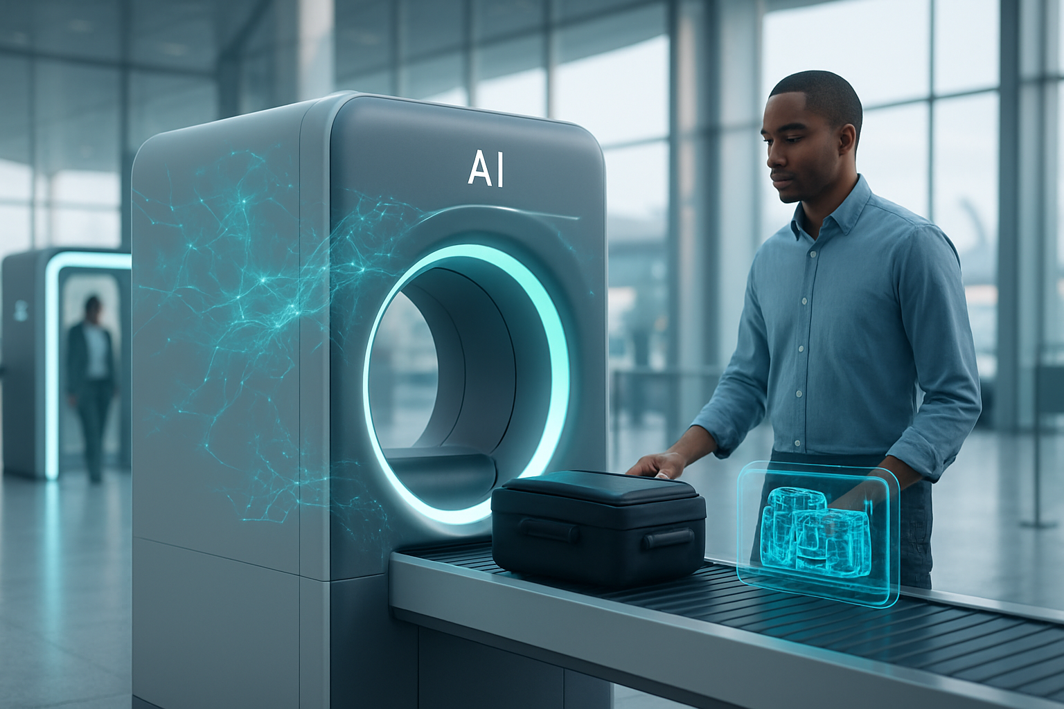
    October 4, 2025 – The skies above the United States are undergoing a profound transformation, ushering in an era where airport security is not only more robust but also remarkably more efficient and passenger-friendly. At the heart of this revolution are advanced AI-powered Computed Tomography (CT) scanners, sophisticated machines that are fundamentally reshaping the experience of air travel. These cutting-edge technologies are moving beyond the limitations of traditional 2D X-ray systems, providing detailed 3D insights into carry-on luggage, enhancing threat detection capabilities, drastically improving operational efficiency, and significantly elevating the overall passenger journey.

    The immediate significance of these AI CT scanners cannot be overstated. By leveraging artificial intelligence to interpret volumetric X-ray images, airports are now equipped with an intelligent defense mechanism that can identify prohibited items with unprecedented precision, including explosives and weapons. This technological leap has begun to untangle the long-standing bottlenecks at security checkpoints, allowing travelers the convenience of keeping laptops, other electronic devices, and even liquids within their bags. The rollout, which began with pilot programs in 2017 and saw significant acceleration from 2018 onwards, continues to gain momentum, promising a future where airport security is a seamless part of the travel experience, rather than a source of stress and delay.

    A Technical Deep Dive into Intelligent Screening

    The core of advanced AI CT scanners lies in the sophisticated integration of computed tomography with powerful artificial intelligence and machine learning (ML) algorithms. Unlike conventional 2D X-ray machines that produce flat, static images often cluttered by overlapping items, CT scanners generate high-resolution, volumetric 3D representations from hundreds of different views as baggage passes through a rotating gantry. This allows security operators to "digitally unpack" bags, zooming in, out, and rotating images to inspect contents from any angle, without physical intervention.

    The AI advancements are critical. Deep neural networks, trained on vast datasets of X-ray images, enable these systems to recognize threat characteristics based on shape, texture, color, and density. This leads to Automated Prohibited Item Detection Systems (APIDS), which leverage machine learning to automatically identify a wide range of prohibited items, from weapons and explosives to narcotics. Companies like SeeTrue and ScanTech AI (with its Sentinel platform) are at the forefront of developing such AI, continuously updating their databases with new threat profiles. Technical specifications include automatic explosives detection (EDS) capabilities that meet stringent regulatory standards (e.g., ECAC EDS CB C3 and TSA APSS v6.2 Level 1), and object recognition software (like Smiths Detection's iCMORE or Rapiscan's ScanAI) that highlights specific prohibited items. These systems significantly increase checkpoint throughput, potentially doubling it, by eliminating the need to remove items and by reducing false alarms, with some conveyors operating at speeds up to 0.5 m/s.

    Initial reactions from the AI research community and industry experts have been largely optimistic, hailing these advancements as a transformative leap. Experts agree that AI-powered CT scanners will drastically improve threat detection accuracy, reduce human errors, and lower false alarm rates. This paradigm shift also redefines the role of security screeners, transitioning them from primary image interpreters to overseers who reinforce AI decisions and focus on complex cases. However, concerns have been raised regarding potential limitations of early AI algorithms, the risk of consistent flaws if AI is not trained properly, and the extensive training required for screeners to adapt to interpreting dynamic 3D images. Privacy and cybersecurity also remain critical considerations, especially as these systems integrate with broader airport datasets.

    Industry Shifts: Beneficiaries, Disruptions, and Market Positioning

    The widespread adoption of AI CT scanners is profoundly reshaping the competitive landscape for AI companies, tech giants, and startups. The most immediate beneficiaries are the manufacturers of these advanced security systems and the developers of the underlying AI algorithms.

    Leading the charge are established security equipment manufacturers such as Smiths Detection (LSE: SMIN), Rapiscan Systems, and Leidos (NYSE: LDOS), who collectively dominate the global market. These companies are heavily investing in and integrating advanced AI into their CT scanners. Analogic Corporation (NASDAQ: ALOG) has also secured substantial contracts with the TSA for its ConneCT systems. Beyond hardware, specialized AI software and algorithm developers like SeeTrue and ScanTech AI are experiencing significant growth, focusing on improving accuracy and reducing false alarms. Companies providing integrated security solutions, such as Thales (EPA: HO) with its biometric and cybersecurity offerings, and training and simulation companies like Renful Premier Technologies, are also poised for expansion.

    For major AI labs and tech giants, this presents opportunities for market leadership and consolidation. These larger entities could develop or license their advanced AI/ML algorithms to scanner manufacturers or offer platforms that integrate CT scanners with broader airport operational systems. The ability to continuously update and improve AI algorithms to recognize evolving threats is a critical competitive factor. Strategic partnerships between airport consortiums and tech companies are also becoming more common to achieve autonomous airport operations.

    The disruption to existing products and services is substantial. Traditional 2D X-ray machines are increasingly becoming obsolete, replaced by superior 3D CT technology. This fundamentally alters long-standing screening procedures, such as the requirement to remove laptops and liquids, minimizing manual inspections. Consequently, the roles of security staff are evolving, necessitating significant retraining and upskilling. Airports must also adapt their infrastructure and operational planning to accommodate the larger CT scanners and new workflows, which can cause short-term disruptions. Companies will compete on technological superiority, continuous AI innovation, enhanced passenger experience, seamless integration capabilities, and global scalability, all while demonstrating strong return on investment.

    Wider Significance: AI's Footprint in Critical Infrastructure

    The deployment of advanced AI CT scanners in airport security is more than just a technological upgrade; it's a significant marker in the broader AI landscape, signaling a deeper integration of intelligent systems into critical infrastructure. This trend aligns with the wider adoption of AI across the aviation industry, from air traffic management and cybersecurity to predictive maintenance and customer service. The US Department of Homeland Security's framework for AI in critical infrastructure underscores this shift towards leveraging AI for enhanced security, resilience, and efficiency.

    In terms of security, the move from 2D to 3D imaging, coupled with AI's analytical power, is a monumental leap. It significantly improves the ability to detect concealed threats and identify suspicious patterns, moving aviation security from a reactive to a more proactive stance. This continuous learning capability, where AI algorithms adapt to new threat data, is a hallmark of modern AI breakthroughs. However, this transformative journey also brings forth critical concerns. Privacy implications arise from the detailed images and the potential integration with biometric data; while the TSA states data is not retained for long, public trust hinges on transparency and robust privacy protection.

    Ethical considerations, particularly algorithmic bias, are paramount. Reports of existing full-body scanners causing discomfort for people of color and individuals with religious head coverings highlight the need for a human-centered design approach to avoid unintentional discrimination. The ethical limits of AI in assessing human intent also remain a complex area. Furthermore, the automation offered by AI CT scanners raises concerns about job displacement for human screeners. While AI can automate repetitive tasks and create new roles focused on oversight and complex decision-making, the societal impact of workforce transformation must be carefully managed. The high cost of implementation and the logistical challenges of widespread deployment also remain significant hurdles.

    Future Horizons: A Glimpse into Seamless Travel

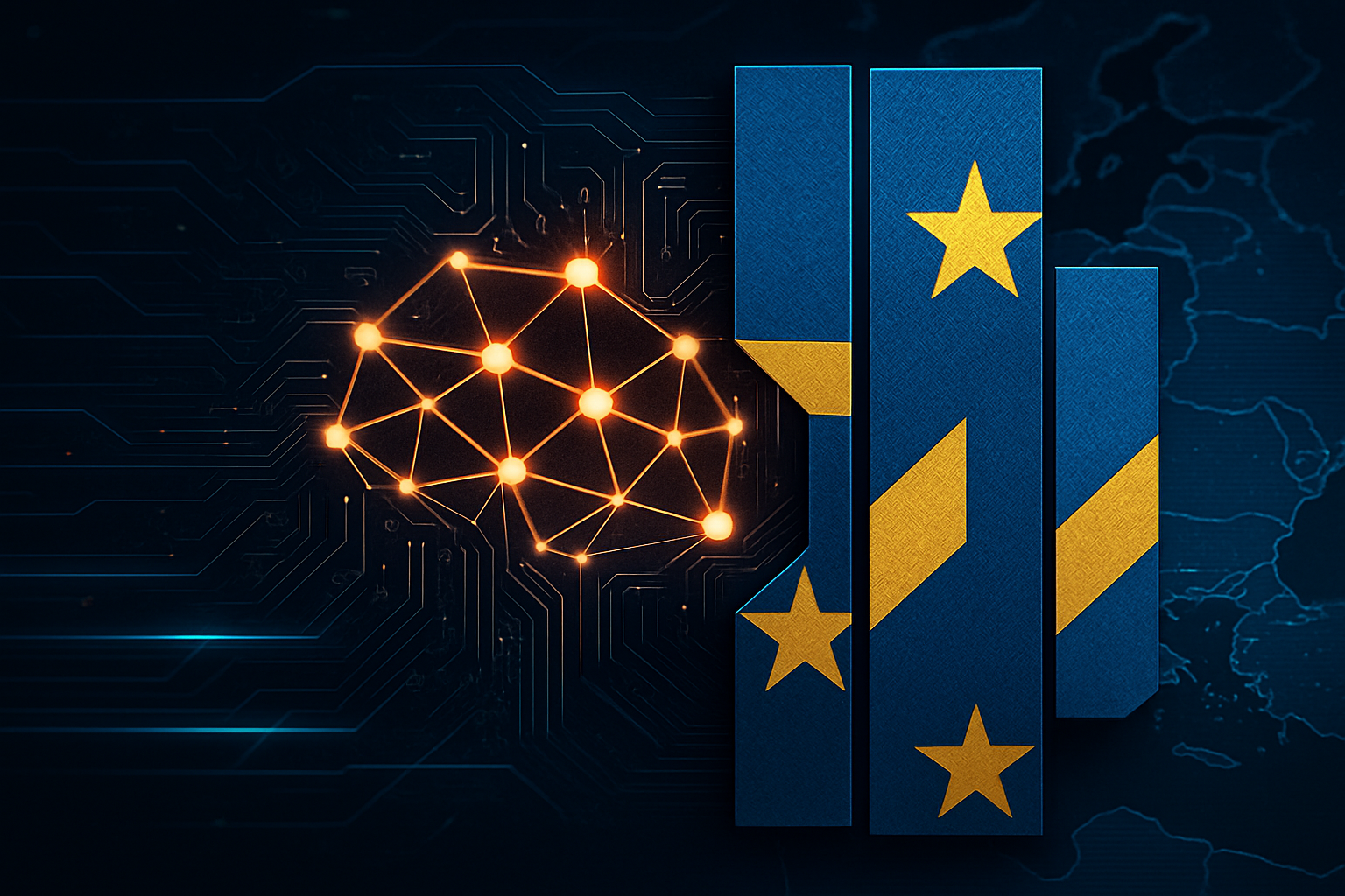
    Looking ahead, the evolution of AI CT scanners in airport security promises a future where air travel is characterized by unparalleled efficiency and convenience. In the near term, we can expect continued refinement of AI algorithms, leading to even greater accuracy in threat detection and a further reduction in false alarms. The European Union's mandate for CT scanners by 2026 and the TSA's ongoing deployment efforts underscore the rapid adoption. Passengers will increasingly experience the benefit of keeping all items in their bags, with some airports already trialing "walk-through" security scanners where bags are scanned alongside passengers.

    Long-term developments envision fully automated and self-service checkpoints where AI handles automatic object recognition, enabling "alarm-only" viewing of X-ray images. This could lead to security experiences as simple as walking along a travelator, with only flagged bags diverted. AI systems will also advance to predictive analytics and behavioral analysis, moving beyond object identification to anticipating risks by analyzing passenger data and behavior patterns. The integration with biometrics and digital identities, creating a comprehensive, frictionless travel experience from check-in to boarding, is also on the horizon. The TSA is exploring remote screening capabilities to further optimize operations.

    Potential applications include advanced Automated Prohibited Item Detection Systems (APIDS) that significantly reduce operator scanning time, and AI-powered body scanning that pinpoints threats without physical pat-downs. Challenges remain, including the substantial cost of deployment, the need for vast quantities of high-quality data to train AI, and the ongoing battle against algorithmic bias and cybersecurity threats. Experts predict that AI, biometric security, and CT scanners will become standard features globally, with the market for aviation security body scanners projected to reach USD 4.44 billion by 2033. The role of security personnel will fundamentally shift to overseeing AI, and a proactive, multi-layered security approach will become the norm, crucial for detecting evolving threats like 3D-printed weapons.

    A New Chapter in Aviation Security

    The advent of advanced AI CT scanners marks a pivotal moment in the history of aviation security and the broader application of artificial intelligence. These intelligent systems are not merely incremental improvements; they represent a fundamental paradigm shift, delivering enhanced threat detection accuracy, significantly improved passenger convenience, and unprecedented operational efficiency. The ability of AI to analyze complex 3D imagery and detect threats faster and more reliably than human counterparts highlights its growing capacity to augment and, in specific data-intensive tasks, even surpass human performance. This firmly positions AI as a critical enabler for a more proactive and intelligent security posture in critical infrastructure.

    The long-term impact promises a future where security checkpoints are no longer the dreaded bottlenecks of air travel but rather seamless, integrated components of a streamlined journey. This will likely lead to the standardization of advanced screening technologies globally, potentially lifting long-standing restrictions on liquids and electronics. However, this transformative journey also necessitates continuous vigilance regarding cybersecurity, data privacy, and the ethical implications of AI, particularly concerning potential biases and the evolving roles for human security personnel.

    In the coming weeks and months, travelers and industry observers alike should watch for the accelerated deployment of these CT scanners in major international airports, particularly as deadlines like the UK's June 2024 target for major airports and the EU's 2026 mandate approach. Keep an eye on regulatory adjustments, as governments begin to formally update carry-on rules in response to these advanced capabilities. Monitoring performance metrics, such as reported reductions in wait times and improvements in passenger satisfaction, will be crucial indicators of success. Finally, continued advancements in AI algorithms and their integration with other cutting-edge security technologies will signal the ongoing evolution towards a truly seamless and intelligent air travel experience.


    This content is intended for informational purposes only and represents analysis of current AI developments.

    TokenRing AI delivers enterprise-grade solutions for multi-agent AI workflow orchestration, AI-powered development tools, and seamless remote collaboration platforms. For more information, visit https://www.tokenring.ai/.

  • The New Frontier: Advanced Packaging Technologies Revolutionize Semiconductors and Power the AI Era

    The New Frontier: Advanced Packaging Technologies Revolutionize Semiconductors and Power the AI Era

    In an era where the insatiable demand for computational power seems limitless, particularly with the explosive growth of Artificial Intelligence, the semiconductor industry is undergoing a profound transformation. The traditional path of continually shrinking transistors, long the engine of Moore's Law, is encountering physical and economic limitations. As a result, a new frontier in chip manufacturing – advanced packaging technologies – has emerged as the critical enabler for the next generation of high-performance, energy-efficient, and compact electronic devices. This paradigm shift is not merely an incremental improvement; it is fundamentally redefining how chips are designed, manufactured, and integrated, becoming the indispensable backbone for the AI revolution.

    Advanced packaging's immediate significance lies in its ability to overcome these traditional scaling challenges by integrating multiple components into a single, cohesive package, moving beyond the conventional single-chip model. This approach is vital for applications such as AI, High-Performance Computing (HPC), 5G, autonomous vehicles, and the Internet of Things (IoT), all of which demand rapid data exchange, immense computational power, low latency, and superior energy efficiency. The importance of advanced packaging is projected to grow exponentially, with its market share expected to double by 2030, outpacing the broader chip industry and solidifying its role as a strategic differentiator in the global technology landscape.

    Beyond the Monolith: Technical Innovations Driving the New Chip Era

    Advanced packaging encompasses a suite of sophisticated manufacturing processes that combine multiple semiconductor dies, or "chiplets," into a single, high-performance package, optimizing performance, power, area, and cost (PPAC). Unlike traditional monolithic integration, where all components are fabricated on a single silicon die (System-on-Chip or SoC), advanced packaging allows for modular, heterogeneous integration, offering significant advantages.

    Key Advanced Packaging Technologies:

    • 2.5D Packaging: This technique places multiple semiconductor dies side-by-side on a passive silicon interposer within a single package. The interposer acts as a high-density wiring substrate, providing fine wiring patterns and high-bandwidth interconnections, bridging the fine-pitch capabilities of integrated circuits with the coarser pitch of the assembly substrate. Through-Silicon Vias (TSVs), vertical electrical connections passing through the silicon interposer, connect the dies to the package substrate. A prime example is High-Bandwidth Memory (HBM) used in NVIDIA Corporation (NASDAQ: NVDA) H100 AI chips, where DRAM is placed adjacent to logic chips on an interposer, enabling rapid data exchange.
    • 3D Packaging (3D ICs): Representing the highest level of integration density, 3D packaging involves vertically stacking multiple semiconductor dies or wafers. TSVs are even more critical here, providing ultra-short, high-performance vertical interconnections between stacked dies, drastically reducing signal delays and power consumption. This technique is ideal for applications demanding extreme density and efficient heat dissipation, such as high-end GPUs and FPGAs, directly addressing the "memory wall" problem by boosting memory bandwidth and reducing latency for memory-intensive AI workloads.
    • Chiplets: Chiplets are small, specialized, unpackaged dies that can be assembled into a single package. This modular approach disaggregates a complex SoC into smaller, functionally optimized blocks. Each chiplet can be manufactured using the most suitable process node (e.g., a 3nm logic chiplet with a 28nm I/O chiplet), leading to "heterogeneous integration." High-speed, low-power die-to-die interconnects, increasingly governed by standards like Universal Chiplet Interconnect Express (UCIe), are crucial for seamless communication between chiplets. Chiplets offer advantages in cost reduction (improved yield), design flexibility, and faster time-to-market.
    • Fan-Out Wafer-Level Packaging (FOWLP): In FOWLP, individual dies are diced, repositioned on a temporary carrier wafer, and then molded with an epoxy compound to form a "reconstituted wafer." A Redistribution Layer (RDL) is then built atop this molded area, fanning out electrical connections beyond the original die area. This eliminates the need for a traditional package substrate or interposer, leading to miniaturization, cost efficiency, and improved electrical performance, making it a cost-effective solution for high-volume consumer electronics and mobile devices.

    These advanced techniques fundamentally differ from monolithic integration by enabling superior performance, bandwidth, and power efficiency through optimized interconnects and modular design. They significantly improve manufacturing yield by allowing individual functional blocks to be tested before integration, reducing costs associated with large, complex dies. Furthermore, they offer unparalleled design flexibility, allowing for the combination of diverse functionalities and process nodes within a single package, a "Lego building block" approach to chip design.

    The initial reaction from the semiconductor and AI research community has been overwhelmingly positive. Experts emphasize that 3D stacking and heterogeneous integration are "critical" for AI development, directly addressing the "memory wall" bottleneck and enabling the creation of specialized, energy-efficient AI hardware. This shift is seen as fundamental to sustaining innovation beyond Moore's Law and is reshaping the industry landscape, with packaging prowess becoming a key differentiator.

    Corporate Chessboard: Beneficiaries, Disruptors, and Strategic Advantages

    The rise of advanced packaging technologies is dramatically reshaping the competitive landscape across the tech industry, creating new strategic advantages and identifying clear beneficiaries while posing potential disruptions.

    Companies Standing to Benefit:

    • Foundries and Advanced Packaging Providers: Giants like TSMC (NYSE: TSM), Intel Corporation (NASDAQ: INTC), and Samsung Electronics Co., Ltd. (KRX: 005930) are investing billions in advanced packaging capabilities. TSMC's CoWoS (Chip-on-Wafer-on-Substrate) and SoIC (System on Integrated Chips), Intel's Foveros (3D stacking) and EMIB (Embedded Multi-die Interconnect Bridge), and Samsung's SAINT technology are examples of proprietary solutions solidifying their positions as indispensable partners for AI chip production. Their expanding capacity is crucial for meeting the surging demand for AI accelerators.
    • AI Hardware Developers: Companies such as NVIDIA Corporation (NASDAQ: NVDA) and Advanced Micro Devices, Inc. (NASDAQ: AMD) are primary drivers and beneficiaries. NVIDIA's H100 and A100 GPUs leverage 2.5D CoWoS technology, while AMD extensively uses chiplets in its Ryzen and EPYC processors and integrates GPU, CPU, and memory chiplets using advanced packaging in its Instinct MI300A/X series accelerators, achieving unparalleled AI performance.
    • Hyperscalers and Tech Giants: Alphabet Inc. (NASDAQ: GOOGL – Google), Amazon (NASDAQ: AMZN – Amazon Web Services), and Microsoft (NASDAQ: MSFT), which are developing custom AI chips or heavily utilizing third-party accelerators, directly benefit from the performance and efficiency gains. These companies rely on advanced packaging to power their massive data centers and AI services.
    • Semiconductor Equipment Suppliers: Companies like ASML Holding N.V. (NASDAQ: ASML), Lam Research Corporation (NASDAQ: LRCX), and SCREEN Holdings Co., Ltd. (TYO: 7735) are crucial enablers, providing specialized equipment for advanced packaging processes, from deposition and etch to inspection, ensuring the high yields and precision required for cutting-edge AI chips.

    Competitive Implications and Disruption:

    Packaging prowess is now a critical competitive battleground, shifting the industry's focus from solely designing the best chip to effectively integrating and packaging it. Companies with strong foundry ties and early access to advanced packaging capacity gain significant strategic advantages. This shift from monolithic to modular designs alters the semiconductor value chain, with value creation migrating towards companies that can design and integrate complex, system-level chip solutions. This also elevates the role of back-end design and packaging as key differentiators.

    The disruption potential is significant. Older technologies relying solely on 2D scaling will struggle to compete. Faster innovation cycles, fueled by enhanced access to advanced packaging, will transform device capabilities in autonomous systems, industrial IoT, and medical devices. Chiplet technology, in particular, could lower barriers to entry for AI startups, allowing them to innovate faster in specialized AI hardware by leveraging pre-designed components.

    A New Pillar of AI: Broader Significance and Societal Impact

    Advanced packaging technologies are more than just an engineering feat; they represent a new pillar supporting the entire AI ecosystem, complementing and enabling algorithmic advancements. Its significance can be compared to previous hardware milestones that unlocked new eras of AI development.

    Fit into the Broader AI Landscape:

    The current AI landscape, dominated by massive Large Language Models (LLMs) and sophisticated generative AI, demands unprecedented computational power, vast memory bandwidth, and ultra-low latency. Advanced packaging directly addresses these requirements by:

    • Enabling Next-Generation AI Models: It provides the essential physical infrastructure to realize and deploy today's and tomorrow's sophisticated AI models at scale, breaking through bottlenecks in computational power and memory access.
    • Powering Specialized AI Hardware: It allows for the creation of highly optimized AI accelerators (GPUs, ASICs, NPUs) by integrating multiple compute cores, memory interfaces, and specialized accelerators into a single package, essential for efficient AI training and inference.
    • From Cloud to Edge AI: These advancements are critical for HPC and data centers, providing unparalleled speed and energy efficiency for demanding AI workloads. Concurrently, modularity and power efficiency benefit edge AI devices, enabling real-time processing in autonomous systems and IoT.
    • AI-Driven Optimization: AI itself is increasingly used to optimize chiplet-based semiconductor designs, leveraging machine learning for power, performance, and thermal efficiency layouts, creating a virtuous cycle of innovation.

    Broader Impacts and Potential Concerns:

    Broader Impacts: Advanced packaging delivers unparalleled performance enhancements, significantly lower power consumption (chiplet-based designs can offer 30-40% lower energy consumption), and cost advantages through improved manufacturing yields and optimized process node utilization. It also redefines the semiconductor ecosystem, fostering greater collaboration across the value chain and enabling faster time-to-market for new AI hardware.

    Potential Concerns: The complexity and high manufacturing costs of advanced packaging, especially 2.5D and 3D solutions, pose challenges, particularly for smaller enterprises. Thermal management remains a significant hurdle as power density increases. The intricate global supply chain for advanced packaging also introduces new vulnerabilities to disruptions and geopolitical tensions. Furthermore, a shortage of skilled labor capable of managing these sophisticated processes could hinder adoption. The environmental impact of energy-intensive manufacturing processes is another growing concern.

    Comparison to Previous AI Milestones:

    Just as the development of GPUs (e.g., NVIDIA's CUDA in 2006) provided the parallel processing power for the deep learning revolution, advanced packaging provides the essential physical infrastructure to realize and deploy today's sophisticated AI models at scale. While Moore's Law drove AI progress for decades through transistor miniaturization, advanced packaging represents a new paradigm shift, moving from monolithic scaling to modular optimization. It's a fundamental redefinition of how computational power is delivered, offering a level of hardware flexibility and customization crucial for the extreme demands of modern AI, especially LLMs. It ensures the relentless march of AI innovation can continue, pushing past physical constraints that once seemed insurmountable.

    The Road Ahead: Future Developments and Expert Predictions

    The trajectory of advanced packaging technologies points towards a future of even greater integration, efficiency, and specialization, driven by the relentless demands of AI and other cutting-edge applications.

    Expected Near-Term and Long-Term Developments:

    • Near-Term (1-5 years): Expect continued maturation of 2.5D and 3D packaging, with larger interposer areas and the emergence of silicon bridge solutions. Hybrid bonding, particularly copper-copper (Cu-Cu) bonding for ultra-fine pitch vertical interconnects, will become critical for future HBM and 3D ICs. Panel-Level Packaging (PLP) will gain traction for cost-effective, high-volume production, potentially utilizing glass interposers for their fine routing capabilities and tunable thermal expansion. AI will become increasingly integrated into the packaging design process for automation, stress prediction, and optimization.
    • Long-Term (beyond 5 years): Fully modular semiconductor designs dominated by custom chiplets optimized for specific AI workloads are anticipated. Widespread 3D heterogeneous computing, with vertical stacking of GPU tiers, DRAM, and other components, will become commonplace. Co-Packaged Optics (CPO) for ultra-high bandwidth communication will be more prevalent, enhancing I/O bandwidth and reducing energy consumption. Active interposers, containing transistors, are expected to gradually replace passive ones, further enhancing in-package functionality. Advanced packaging will also facilitate the integration of emerging technologies like quantum and neuromorphic computing.

    Potential Applications and Use Cases:

    These advancements are critical enablers for next-generation applications across diverse sectors:

    • High-Performance Computing (HPC) and Data Centers: Powering generative AI, LLMs, and data-intensive workloads with unparalleled speed and energy efficiency.
    • Artificial Intelligence (AI) Accelerators: Creating more powerful and energy-efficient specialized AI chips by integrating CPUs, GPUs, and HBM to overcome memory bottlenecks.
    • Edge AI Devices: Supporting real-time processing in autonomous systems, industrial IoT, consumer electronics, and portable devices due to modularity and power efficiency.
    • 5G and 6G Communications: Shaping future radio access network (RAN) architectures with innovations like antenna-in-package solutions.
    • Autonomous Vehicles: Integrating sensor suites and computing units for processing vast amounts of data while ensuring safety, reliability, and compactness.
    • Healthcare, Quantum Computing, and Neuromorphic Computing: Leveraging advanced packaging for transformative applications in computational efficiency and integration.

    Challenges and Expert Predictions:

    Key challenges include the high manufacturing costs and complexity, particularly for ultra-fine pitch hybrid bonding, and the need for innovative thermal management solutions for increasingly dense packages. Developing new materials to address thermal expansion and heat transfer, along with advanced Electronic Design Automation (EDA) software for complex multi-chip simulations, are also crucial. Supply chain coordination and standardization across the chiplet ecosystem require unprecedented collaboration.

    Experts widely recognize advanced packaging as essential for extending performance scaling beyond traditional transistor miniaturization, addressing the "memory wall," and enabling new, highly optimized heterogeneous computing architectures crucial for modern AI. The market is projected for robust growth, with the package itself becoming a crucial point of innovation. AI will continue to accelerate this shift, not only driving demand but also playing a central role in optimizing design and manufacturing. Strategic partnerships and the boom of Outsourced Semiconductor Assembly and Test (OSAT) providers are expected as companies navigate the immense capital expenditure for cutting-edge packaging.

    The Unsung Hero: A New Era of Innovation

    In summary, advanced packaging technologies are the unsung hero powering the next wave of innovation in semiconductors and AI. They represent a fundamental shift from "More than Moore" to an era where heterogeneous integration and 3D stacking are paramount, pushing the boundaries of what's possible in terms of integration, performance, and efficiency.

    The key takeaways underscore its role in extending Moore's Law, overcoming the "memory wall," enabling specialized AI hardware, and delivering unprecedented performance, power efficiency, and compact form factors. This development is not merely significant; it is foundational, ensuring that hardware innovation keeps pace with the rapid evolution of AI software and applications.

    The long-term impact will see chiplet-based designs become the new standard, sustained acceleration in AI capabilities, widespread adoption of co-packaged optics, and AI-driven design automation. The market for advanced packaging is set for explosive growth, fundamentally reshaping the semiconductor ecosystem and demanding greater collaboration across the value value chain.

    In the coming weeks and months, watch for accelerated adoption of 2.5D and 3D hybrid bonding, the continued maturation of the chiplet ecosystem and UCIe standards, and significant investments in packaging capacity by major players like TSMC (NYSE: TSM), Intel Corporation (NASDAQ: INTC), and Samsung Electronics Co., Ltd. (KRX: 005930). Further innovations in thermal management and novel substrates, along with the increasing application of AI within packaging manufacturing itself, will be critical trends to observe as the industry collectively pushes the boundaries of integration and performance.

    This content is intended for informational purposes only and represents analysis of current AI developments.

    TokenRing AI delivers enterprise-grade solutions for multi-agent AI workflow orchestration, AI-powered development tools, and seamless remote collaboration platforms.
    For more information, visit https://www.tokenring.ai/.

  • Semiconductor Startups Spark a New Era: Billions in Funding Fuel AI’s Hardware Revolution

    Semiconductor Startups Spark a New Era: Billions in Funding Fuel AI’s Hardware Revolution

    The global semiconductor industry is undergoing a profound transformation, driven by an unprecedented surge in investments and a wave of groundbreaking innovations from a vibrant ecosystem of startups. As of October 4, 2025, venture capital is pouring billions into companies that are pushing the boundaries of chip design, interconnectivity, and specialized processing, fundamentally reshaping the future of Artificial Intelligence (AI) and high-performance computing. This dynamic period, marked by significant funding rounds and disruptive technological breakthroughs, signals a new golden era for silicon, poised to accelerate AI development and deployment across every sector.

    This explosion of innovation is directly responding to the insatiable demands of AI, from the colossal computational needs of large language models to the intricate requirements of on-device edge AI. Startups are introducing novel architectures, advanced materials, and revolutionary packaging techniques that promise to overcome the physical limitations of traditional silicon, paving the way for more powerful, energy-efficient, and ubiquitous AI applications. The immediate significance of these developments lies in their potential to unlock unprecedented AI capabilities, foster increased competition, and alleviate critical bottlenecks in data transfer and power consumption that have constrained the industry's growth.

    Detailed Technical Coverage: The Dawn of Specialized AI Hardware

    The core of this semiconductor renaissance lies in highly specialized AI chip architectures and advanced interconnect solutions designed to bypass the limitations of general-purpose CPUs and even traditional GPUs. Companies are innovating across the entire stack, from the foundational materials to the system-level integration.

    Cerebras Systems, for example, continues to redefine high-performance AI computing with its Wafer-Scale Engine (WSE). The latest iteration, WSE-3, fabricated on TSMC's (NYSE: TSM) 5nm process, packs an astounding 4 trillion transistors and 900,000 AI-optimized cores onto a single silicon wafer. This monolithic design dramatically reduces latency and bandwidth limitations inherent in multi-chip GPU clusters, allowing for the training of massive AI models with up to 24 trillion parameters on a single system. Its "Weight Streaming Architecture" disaggregates memory from compute, enabling efficient handling of arbitrarily large parameter counts. While NVIDIA (NASDAQ: NVDA) dominates with its broad ecosystem, Cerebras's specialized approach offers compelling performance advantages for ultra-fast AI inference, challenging the status quo for specific high-end workloads.

    Tenstorrent, led by industry veteran Jim Keller, is championing the open-source RISC-V architecture for efficient and cost-effective AI processing. Their chips, designed with a proprietary mesh topology featuring both general-purpose and specialized RISC-V cores, aim to deliver superior efficiency and lower costs compared to NVIDIA's (NASDAQ: NVDA) offerings, partly by utilizing GDDR6 memory instead of expensive High Bandwidth Memory (HBM). Tenstorrent's upcoming "Black Hole" and "Quasar" processors promise to expand their footprint in both standalone AI and multi-chiplet solutions. This open-source strategy directly challenges proprietary ecosystems like NVIDIA's (NASDAQ: NVDA) CUDA, fostering greater customization and potentially more affordable AI development, though building a robust software environment remains a significant hurdle.

    Beyond compute, power delivery and data movement are critical bottlenecks being addressed. Empower Semiconductor is revolutionizing power management with its Crescendo platform, a vertically integrated power delivery solution that fits directly beneath the processor. This "vertical power delivery" eliminates lateral transmission losses, offering 20x higher bandwidth, 5x higher density, and a more than 10% reduction in power delivery losses compared to traditional methods. This innovation is crucial for sustaining the escalating power demands of next-generation AI processors, ensuring they can operate efficiently and without thermal throttling.

    The "memory wall" and data transfer bottlenecks are being tackled by optical interconnect specialists. Ayar Labs is at the forefront with its TeraPHY™ optical I/O chiplet and SuperNova™ light source, using light to move data at unprecedented speeds. Their technology, which includes the first optical UCIe-compliant chiplet, offers 16 Tbps of bi-directional bandwidth with latency as low as a few nanoseconds and significantly reduced power consumption. Similarly, Celestial AI is advancing a "Photonic Fabric" technology that delivers optical interconnects directly into the heart of the silicon, addressing the "beachfront problem" and enabling memory disaggregation for pooled, high-speed memory access across data centers. These optical solutions are seen as the only viable path to scale performance and power efficiency in large-scale AI and HPC systems, potentially replacing traditional electrical interconnects like NVLink.

    Enfabrica is tackling I/O bottlenecks in massive AI clusters with its "SuperNICs" and memory fabrics. Their Accelerated Compute Fabric (ACF) SuperNIC, Millennium, is a one-chip solution that delivers 8 terabytes per second of bandwidth, uniquely bridging Ethernet and PCIe/CXL technologies. Its EMFASYS AI Memory Fabric System enables elastic, rack-scale memory pooling, allowing GPUs to offload data from limited HBM into shared storage, freeing up HBM for critical tasks and potentially reducing token processing costs by up to 50%. This approach offers a significant uplift in I/O bandwidth and a 75% reduction in node-to-node latency, directly addressing the scaling challenges of modern AI workloads.

    Finally, Black Semiconductor is exploring novel materials, leveraging graphene to co-integrate electronics and optics directly onto chips. Graphene's superior optical, electrical, and thermal properties enable ultra-fast, energy-efficient data transfer over longer distances, moving beyond the physical limitations of copper. This innovative material science holds the promise of fundamentally changing how chips communicate, offering a path to overcome the bandwidth and energy constraints that currently limit inter-chip communication.

    Impact on AI Companies, Tech Giants, and Startups

    The rapid evolution within semiconductor startups is sending ripples throughout the entire AI and tech ecosystem, creating both opportunities and competitive pressures for established giants and emerging players alike.

    Tech giants like NVIDIA (NASDAQ: NVDA), despite its commanding lead with a market capitalization reaching $4.5 trillion as of October 2025, faces intensifying competition. While its vertically integrated stack of GPUs, CUDA software, and networking solutions remains a formidable moat, the rise of specialized AI chips from startups and custom silicon initiatives from its largest customers (Google (NASDAQ: GOOGL), Amazon (NASDAQ: AMZN), Microsoft (NASDAQ: MSFT)) are challenging its dominance. NVIDIA's recent $5 billion investment in Intel (NASDAQ: INTC) and co-development partnership signals a strategic move to secure domestic chip supply, diversify its supply chain, and fuse GPU and CPU expertise to counter rising threats.

    Intel (NASDAQ: INTC) and AMD (NASDAQ: AMD) are aggressively rolling out their own AI accelerators and CPUs to capture market share. AMD's Instinct MI300X chips, integrated by cloud providers like Oracle (NYSE: ORCL) and Google (NASDAQ: GOOGL), position it as a strong alternative to NVIDIA's (NASDAQ: NVDA) GPUs. Intel's (NASDAQ: INTC) manufacturing capabilities, particularly with U.S. government backing and its strategic partnership with NVIDIA (NASDAQ: NVDA), provide a unique advantage in the quest for technological leadership and supply chain resilience.

    Hyperscalers such as Google (NASDAQ: GOOGL) (Alphabet), Amazon (NASDAQ: AMZN) (AWS), and Microsoft (NASDAQ: MSFT) (Azure) are making massive capital investments, projected to exceed $300 billion collectively in 2025, primarily for AI infrastructure. Critically, these companies are increasingly developing custom silicon (ASICs) like Google's TPUs and Axion CPUs, Microsoft's Azure Maia 100 AI Accelerator, and Amazon's Trainium2. This vertical integration strategy aims to reduce reliance on external suppliers, optimize performance for specific AI workloads, achieve cost efficiency, and gain greater control over their cloud platforms, directly disrupting the market for general-purpose AI hardware.

    For other AI companies and startups, these developments offer a mixed bag. They stand to benefit from the increasing availability of diverse, specialized, and potentially more cost-effective hardware, allowing them to access powerful computing resources without the prohibitive costs of building their own. The shift towards open-source architectures like RISC-V also fosters greater flexibility and innovation. However, the complexity of optimizing AI models for various hardware architectures presents a new challenge, and the capital-intensive nature of the AI chip industry means startups often require significant venture capital to compete effectively. Strategic partnerships with tech giants or cloud providers become crucial for long-term viability.

    Wider Significance: The AI Cold War and a Sustainable Future

    The profound investments and innovations in semiconductor startups carry a wider significance that extends into geopolitical arenas, environmental concerns, and the very trajectory of AI development. These advancements are not merely technological improvements; they are foundational shifts akin to past milestones, enabling a new era of AI.

    These innovations fit squarely into the broader AI landscape, acting as the essential hardware backbone for sophisticated AI systems. The trend towards specialized AI chips (GPUs, TPUs, ASICs, NPUs) optimized for parallel processing is crucial for scaling machine learning and deep learning models. Furthermore, the push for Edge AI — processing data locally on devices — is being directly enabled by these startups, reducing latency, conserving bandwidth, and enhancing privacy for applications ranging from autonomous vehicles and IoT to industrial automation. Innovations in advanced packaging, new materials like graphene, and even nascent neuromorphic and quantum computing are pushing beyond the traditional limits of Moore's Law, ensuring continued breakthroughs in AI capabilities.

    The impacts are pervasive across numerous sectors. In healthcare, enhanced AI capabilities, powered by faster chips, accelerate drug discovery and medical imaging. In transportation, autonomous vehicles and ADAS rely heavily on these advanced chips for real-time sensor data processing. Industrial automation, consumer electronics, and data centers are all experiencing transformative shifts due to more powerful and efficient AI hardware.

    However, this technological leap comes with significant concerns. Energy consumption is a critical issue; AI data centers already consume a substantial portion of global electricity, with projections indicating a sharp increase in CO2 emissions from AI accelerators. The urgent need for more sustainable and energy-efficient chip designs and cooling solutions is paramount. The supply chain remains incredibly vulnerable, with a heavy reliance on a few key manufacturers like TSMC (NYSE: TSM) in Taiwan. This concentration, exacerbated by geopolitical tensions, raw material shortages, and export restrictions, creates strategic risks.

    Indeed, semiconductors have become strategic assets in an "AI Cold War," primarily between the United States and China. Nations are prioritizing technological sovereignty, leading to export controls (e.g., US restrictions on advanced semiconductor technologies to China), trade barriers, and massive investments in domestic production (e.g., US CHIPS Act, European Chips Act). This geopolitical rivalry risks fragmenting the global technology ecosystem, potentially leading to duplicated supply chains, higher costs, and a slower pace of global innovation.

    Comparing this era to previous AI milestones, the current semiconductor innovations are as foundational as the development of GPUs and the CUDA platform in enabling the deep learning revolution. Just as parallel processing capabilities unlocked the potential of neural networks, today's advanced packaging, specialized AI chips, and novel interconnects are providing the physical infrastructure to deploy increasingly complex and sophisticated AI models at an unprecedented scale. This creates a virtuous cycle where hardware advancements enable more complex AI, which in turn demands and helps create even better hardware.

    Future Developments: A Trillion-Dollar Market on the Horizon

    The trajectory of AI-driven semiconductor innovation promises a future of unprecedented computational power and ubiquitous intelligence, though significant challenges remain. Experts predict a dramatic acceleration of AI/ML adoption, with the market expanding from $46.3 billion in 2024 to $192.3 billion by 2034, and the global semiconductor market potentially reaching $1 trillion by 2030.

    In the near-term (2025-2028), we can expect to see AI-driven tools revolutionize chip design and verification, compressing development cycles from months to days. AI-powered Electronic Design Automation (EDA) tools will automate tasks, predict errors, and optimize layouts, leading to significant gains in power efficiency and design productivity. Manufacturing optimization will also be transformed, with AI enhancing predictive maintenance, defect detection, and real-time process control in fabs. The expansion of advanced process node capacity (7nm and below, including 2nm) will accelerate, driven by the explosive demand for AI accelerators and High Bandwidth Memory (HBM).

    Looking further ahead (beyond 2028), the vision includes fully autonomous manufacturing facilities and AI-designed chips created with minimal human intervention. We may witness the emergence of novel computing paradigms such as neuromorphic computing, which mimics the human brain for ultra-efficient processing, and the continued advancement of quantum computing. Advanced packaging technologies like 3D stacking and chiplets will become even more sophisticated, overcoming traditional silicon scaling limits and enabling greater customization. The integration of Digital Twins for R&D will accelerate innovation and optimize performance across the semiconductor value chain.

    These advancements will power a vast array of new applications. Edge AI and IoT will see specialized, low-power chips enabling smarter devices and real-time processing in robotics and industrial automation. High-Performance Computing (HPC) and data centers will continue to be the lifeblood for generative AI, with semiconductor sales in this market projected to grow at an 18% CAGR from 2025 to 2030. The automotive sector will rely heavily on AI-driven chips for electrification and autonomous driving. Photonics, augmented/virtual reality (AR/VR), and robotics will also be significant beneficiaries.

    However, critical challenges must be addressed. Power consumption and heat dissipation remain paramount concerns for AI workloads, necessitating continuous innovation in energy-efficient designs and advanced cooling solutions. The manufacturing complexities and costs of sub-11nm chips are soaring, with new fabs exceeding $20 billion in 2024 and projected to reach $40 billion by 2028. A severe and intensifying global talent shortage in semiconductor design and manufacturing, potentially exceeding one million additional skilled professionals by 2030, poses a significant threat. Geopolitical tensions and supply chain vulnerabilities will continue to necessitate strategic investments and diversification.

    Experts predict a continued "arms race" in chip development, with heavy investment in advanced packaging and AI integration into design and manufacturing. Strategic partnerships between chipmakers, AI developers, and material science companies will be crucial. While NVIDIA (NASDAQ: NVDA) currently dominates, competition from AMD (NASDAQ: AMD), Intel (NASDAQ: INTC), and Qualcomm (NASDAQ: QCOM) will intensify, particularly in specialized architectures and edge AI segments.

    Comprehensive Wrap-up: Forging the Future of AI

    The current wave of investments and emerging innovations within semiconductor startups represents a pivotal moment in AI history. The influx of billions of dollars, particularly from Q3 2024 to Q3 2025, underscores an industry-wide recognition that advanced AI demands a fundamentally new approach to hardware. Startups are leading the charge in developing specialized AI chips, revolutionary optical interconnects, efficient power delivery solutions, and open-source architectures like RISC-V, all designed to overcome the critical bottlenecks of processing power, energy consumption, and data transfer.

    These developments are not merely incremental; they are fundamentally reshaping how AI systems are designed, deployed, and scaled. By providing the essential hardware foundation, these innovations are enabling the continued exponential growth of AI models, pushing towards more sophisticated, energy-efficient, and ubiquitous AI applications. The ability to process data locally at the edge, for instance, is crucial for autonomous vehicles and IoT devices, bringing AI capabilities closer to the source of data and unlocking new possibilities. This symbiotic relationship between AI and semiconductor innovation is accelerating progress and redefining the possibilities of what AI can achieve.

    The long-term impact will be transformative, leading to sustained AI advancement, the democratization of chip design through AI-powered tools, and a concerted effort towards energy efficiency and sustainability in computing. We can expect more diversified and resilient supply chains driven by geopolitical motivations, and potentially entirely new computing paradigms emerging from RISC-V and quantum technologies. The semiconductor industry, projected for substantial growth, will continue to be the primary engine of the AI economy.

    In the coming weeks and months, watch for the commercialization and market adoption of these newly funded products, particularly in optical interconnects and specialized AI accelerators. Performance benchmarks will be crucial indicators of market leadership, while the continued development of the RISC-V ecosystem will signal its long-term viability. Keep an eye on further funding rounds, potential M&A activity, and new governmental policies aimed at bolstering domestic semiconductor capabilities. The ongoing integration of AI into chip design (EDA) and advancements in advanced packaging will also be key areas to monitor, as they directly impact the speed and cost of innovation. The semiconductor startup landscape remains a vibrant hub, laying the groundwork for an AI-driven future that is more powerful, efficient, and integrated into every facet of our lives.


    This content is intended for informational purposes only and represents analysis of current AI developments.

    TokenRing AI delivers enterprise-grade solutions for multi-agent AI workflow orchestration, AI-powered development tools, and seamless remote collaboration platforms. For more information, visit https://www.tokenring.ai/.

  • Intel’s Phoenix Moment: Foundry Push and Aggressive Roadmap Fuel Bid to Reclaim Chip Dominance

    Intel (NASDAQ: INTC) is in the midst of an audacious and critical turnaround effort, dubbed "IDM 2.0," aiming to resurrect its once-unquestioned leadership in the semiconductor industry. Under the strategic direction of CEO Lip-Bu Tan, who took the helm in March 2025, the company is making a monumental bet on transforming itself into a major global provider of foundry services through Intel Foundry Services (IFS). This initiative, coupled with an aggressive process technology roadmap and substantial investments, is designed to reclaim market share, diversify revenue, and solidify its position as a cornerstone of the global chip supply chain by the end of the decade.

    The immediate significance of this pivot cannot be overstated. With geopolitical tensions highlighting the fragility of a concentrated chip manufacturing base, Intel's push to offer advanced foundry capabilities in the U.S. and Europe provides a crucial alternative. Key customer wins, including a landmark commitment from Microsoft (NASDAQ: MSFT) for its 18A process, and reported early-stage talks with long-time rival AMD (NASDAQ: AMD), signal growing industry confidence. As of October 2025, Intel is not just fighting for survival; it's actively charting a course to re-establish itself at the vanguard of semiconductor innovation and production.

    Rebuilding from the Core: Intel's IDM 2.0 and Foundry Ambitions

    Intel's IDM 2.0 strategy, first unveiled in March 2021, is a comprehensive blueprint to revitalize the company's fortunes. It rests on three fundamental pillars: maintaining internal manufacturing for the majority of its core products, strategically increasing its use of third-party foundries for certain components, and, most critically, establishing Intel Foundry Services (IFS) as a leading global foundry. This last pillar signifies Intel's transformation from a solely integrated device manufacturer to a hybrid model that also serves external clients, a direct challenge to industry titans like Taiwan Semiconductor Manufacturing Company (TSMC) (NYSE: TSM) and Samsung (KRX: 005930).

    A central component of this strategy is an aggressive process technology roadmap, famously dubbed "five nodes in four years" (5N4Y). This ambitious timeline aims to achieve "process performance leadership" by 2025. The roadmap includes Intel 7 (already in high-volume production), Intel 4 (in production since H2 2022), Intel 3 (now in high volume), Intel 20A (ushering in the "Angstrom era" with RibbonFET and PowerVia technologies in 2024), and Intel 18A, slated for volume manufacturing in late 2025. Intel is confident that the 18A node will be the cornerstone of its return to process leadership. These advancements are complemented by significant investments in advanced packaging technologies like EMIB and Foveros, and pioneering work on glass substrates for future high-performance computing.

    The transition to an "internal foundry model" in Q1 2024 further solidifies IFS's foundation. By operating its manufacturing groups with standalone profit and loss (P&L) statements, Intel effectively created the industry's second-largest foundry by volume from internal customers, de-risking the venture for external clients. This move provides a substantial baseline volume, making IFS a more attractive and stable partner for other chip designers. The technical capabilities offered by IFS extend beyond just leading-edge nodes, encompassing advanced packaging, design services, and robust intellectual property (IP) ecosystems, including partnerships with Arm (NASDAQ: ARM) for optimizing its processor cores on Intel's advanced nodes.

    Initial reactions from the AI research community and industry experts have been cautiously optimistic, particularly given the significant customer commitments. The validation from a major player like Microsoft, choosing Intel's 18A process for its in-house designed AI accelerators (Maia 100) and server CPUs (Cobalt 100), is a powerful testament to Intel's progress. Furthermore, the rumored early-stage talks with AMD regarding potential manufacturing could mark a pivotal moment, providing AMD with supply chain diversification and substantially boosting IFS's credibility and order book. These developments suggest that Intel's aggressive technological push is beginning to yield tangible results and gain traction in a highly competitive landscape.

    Reshaping the Semiconductor Ecosystem: Competitive Implications and Market Shifts

    Intel's strategic pivot into the foundry business carries profound implications for the entire semiconductor industry, potentially reshaping competitive dynamics for tech giants, AI companies, and startups alike. The most direct beneficiaries of a successful IFS would be customers seeking a geographically diversified and technologically advanced manufacturing alternative to the current duopoly of TSMC and Samsung. Companies like Microsoft, already committed to 18A, stand to gain enhanced supply chain resilience and potentially more favorable terms as Intel vies for market share. The U.S. government is also a customer for 18A through the RAMP and RAMP-C programs, highlighting the strategic national importance of Intel's efforts.

    The competitive implications for major AI labs and tech companies are significant. As AI workloads demand increasingly specialized and high-performance silicon, having another leading-edge foundry option could accelerate innovation. For companies designing their own AI chips, such as Google (NASDAQ: GOOGL), Amazon (NASDAQ: AMZN), and potentially even Nvidia (NASDAQ: NVDA) (which has reportedly invested in Intel and partnered on custom x86 CPUs for AI infrastructure), IFS could offer a valuable alternative, reducing reliance on a single foundry. This increased competition among foundries could lead to better pricing, faster technology development, and more customized solutions for chip designers.

    Potential disruption to existing products or services could arise if Intel's process technology roadmap truly delivers on its promise of leadership. If Intel 18A indeed achieves superior performance-per-watt by late 2025, it could enable new levels of efficiency and capability for chips manufactured on that node, potentially putting pressure on products built on rival processes. For instance, if Intel's internal CPUs manufactured on 18A outperform competitors, it could help regain market share in the lucrative server and PC segments where Intel has seen declines, particularly against AMD.

    From a market positioning standpoint, Intel aims to become the world's second-largest foundry by revenue by 2030. This ambitious goal directly challenges Samsung's current position and aims to chip away at TSMC's dominance. Success in this endeavor would not only diversify Intel's revenue streams but also provide strategic advantages by giving Intel deeper insights into the design needs of its customers, potentially informing its own product development. The reported engagement with MediaTek (TPE: 2454) for Intel 16nm and Cisco (NASDAQ: CSCO) further illustrates the breadth of industries Intel Foundry Services is targeting, from mobile to networking.

    Broader Significance: Geopolitics, Supply Chains, and the Future of Chipmaking

    Intel's turnaround efforts, particularly its foundry ambitions, resonate far beyond the confines of its balance sheet; they carry immense wider significance for the broader AI landscape, global supply chains, and geopolitical stability. The push for geographically diversified chip manufacturing, with new fabs planned or under construction in Arizona, Ohio, and Germany, directly addresses the vulnerabilities exposed by an over-reliance on a single region for advanced semiconductor production. This initiative is strongly supported by government incentives like the U.S. CHIPS Act and similar European programs, underscoring its national and economic security importance.

    The impacts of a successful IFS are multifaceted. It could foster greater innovation by providing more avenues for chip designers to bring their ideas to fruition. For AI, where specialized hardware is paramount, a competitive foundry market ensures that cutting-edge designs can be manufactured efficiently and securely. This decentralization of advanced manufacturing could also mitigate the risks of future supply chain disruptions, which have plagued industries from automotive to consumer electronics in recent years. Furthermore, it represents a significant step towards "reshoring" critical manufacturing capabilities to Western nations.

    Potential concerns, however, remain. The sheer capital expenditure required for Intel's aggressive roadmap is staggering, placing significant financial pressure on the company. Execution risk is also high; achieving "five nodes in four years" is an unprecedented feat, and any delays could undermine market confidence. The profitability of its foundry operations, especially when competing against highly optimized and established players like TSMC, will be a critical metric to watch. Geopolitical tensions, while driving the need for diversification, could also introduce complexities if trade relations shift.

    Comparisons to previous AI milestones and breakthroughs are apt. Just as the development of advanced algorithms and datasets has fueled AI's progress, the availability of cutting-edge, reliable, and geographically diverse hardware manufacturing is equally crucial. Intel's efforts are not just about regaining market share; they are about building the foundational infrastructure upon which the next generation of AI innovation will be built. This mirrors historical moments when access to new computing paradigms, from mainframes to cloud computing, unlocked entirely new technological frontiers.

    The Road Ahead: Anticipated Developments and Lingering Challenges

    Looking ahead, the semiconductor industry will closely watch several key developments stemming from Intel's turnaround. In the near term, the successful ramp-up of Intel 18A in late 2025 will be paramount. Any indication of delays or performance issues could significantly impact market perception and customer commitments. The continued progress of key customer tape-outs, particularly from Microsoft and potential engagements with AMD, will serve as crucial validation points. Further announcements regarding new IFS customers or expansions of existing partnerships will also be closely scrutinized.

    Long-term, the focus will shift to the profitability and sustained growth of IFS. Experts predict that Intel will need to demonstrate consistent execution on its process roadmap beyond 18A to maintain momentum and attract a broader customer base. The development of next-generation packaging technologies and specialized process nodes for AI accelerators will be critical for future applications. Potential use cases on the horizon include highly integrated chiplets for AI supercomputing, custom silicon for edge AI devices, and advanced processors for quantum computing, all of which could leverage Intel's foundry capabilities.

    However, significant challenges need to be addressed. Securing a steady stream of external foundry customers beyond the initial anchor clients will be crucial for scaling IFS. Managing the complex interplay between Intel's internal product groups and its external foundry customers, ensuring fair allocation of resources and capacity, will also be a delicate balancing act. Furthermore, talent retention amidst ongoing restructuring and the intense global competition for semiconductor engineering expertise remains a persistent hurdle. The global economic climate and potential shifts in government support for domestic chip manufacturing could also influence Intel's trajectory.

    Experts predict that while Intel faces an uphill battle, its aggressive investments and strategic focus on foundry services position it for a potential resurgence. The industry will be observing whether Intel can not only achieve process leadership but also translate that into sustainable market share gains and profitability. The coming years will determine if Intel's multi-billion-dollar gamble pays off, transforming it from a struggling giant into a formidable player in the global foundry market.

    A New Chapter for an Industry Icon: Assessing Intel's Rebirth

    Intel's strategic efforts represent one of the most significant turnaround attempts in recent technology history. The key takeaways underscore a company committed to a radical transformation: a bold "IDM 2.0" strategy, an aggressive "five nodes in four years" process roadmap culminating in 18A leadership by late 2025, and a monumental pivot into foundry services with significant customer validation from Microsoft and reported interest from AMD. These initiatives are not merely incremental changes but a fundamental reorientation of Intel's business model and technological ambitions.

    The significance of this development in semiconductor history cannot be overstated. It marks a potential shift in the global foundry landscape, offering a much-needed alternative to the concentrated manufacturing base. If successful, Intel's IFS could enhance supply chain resilience, foster greater innovation, and solidify Western nations' access to cutting-edge chip production. This endeavor is a testament to the strategic importance of semiconductors in the modern world, where technological leadership is inextricably linked to economic and national security.

    Final thoughts on the long-term impact suggest that a revitalized Intel, particularly as a leading foundry, could usher in a new era of competition and collaboration in the chip industry. It could accelerate the development of specialized AI hardware, enable new computing paradigms, and reinforce the foundational technology for countless future innovations. The successful integration of its internal product groups with its external foundry business will be crucial for sustained success.

    In the coming weeks and months, the industry will be watching closely for further announcements regarding Intel 18A's progress, additional customer wins for IFS, and the financial performance of Intel's manufacturing division under the new internal foundry model. Any updates on the rumored AMD partnership would also be a major development. Intel's journey is far from over, but as of October 2025, the company has laid a credible foundation for its ambitious bid to reclaim its place at the pinnacle of the semiconductor world.

    This content is intended for informational purposes only and represents analysis of current AI developments.

    TokenRing AI delivers enterprise-grade solutions for multi-agent AI workflow orchestration, AI-powered development tools, and seamless remote collaboration platforms.
    For more information, visit https://www.tokenring.ai/.

  • Geopolitics and Chips: Navigating the Turbulent Semiconductor Supply Chain

    Geopolitics and Chips: Navigating the Turbulent Semiconductor Supply Chain

    The global semiconductor industry, the bedrock of modern technology and the engine driving the artificial intelligence revolution, finds itself at the epicenter of an unprecedented geopolitical maelstrom. Far from a mere commercial enterprise, semiconductors have unequivocally become strategic assets, with nations worldwide scrambling for technological supremacy and self-sufficiency. This escalating tension, fueled by export controls, trade restrictions, and a fierce competition for advanced manufacturing capabilities, is creating widespread disruptions, escalating costs, and fundamentally reshaping the intricate global supply chain. The ripple effects are profound, threatening the stability of the entire tech sector and, most critically, the future trajectory of AI development and deployment.

    This turbulent environment signifies a paradigm shift where geopolitical alignment increasingly dictates market access and operational strategies, transforming a once globally integrated network into a battleground for technological dominance. For the burgeoning AI industry, which relies insatiably on cutting-edge, high-performance semiconductors, these disruptions are particularly critical. Delays, shortages, and increased costs for these essential components risk slowing the pace of innovation, exacerbating the digital divide, and potentially fragmenting AI development along national lines. The world watches as the delicate balance of chip production and distribution hangs in the balance, with immediate and long-term implications for global technological progress.

    The Technical Fault Lines: How Geopolitics Reshapes Chip Production and Distribution

    The intricate dance of semiconductor manufacturing, once governed primarily by economic efficiency and global collaboration, is now dictated by the sharp edges of geopolitical strategy. Specific trade policies, escalating international rivalries, and the looming specter of regional conflicts are not merely inconveniencing the industry; they are fundamentally altering its technical architecture, distribution pathways, and long-term stability in ways unprecedented in its history.

    At the forefront of these technical disruptions are export controls, wielded as precision instruments to impede technological advancement. The most potent example is the restriction on advanced lithography equipment, particularly Extreme Ultraviolet (EUV) and advanced Deep Ultraviolet (DUV) systems from companies like ASML (AMS:ASML) in the Netherlands. These highly specialized machines, crucial for etching transistor patterns smaller than 7 nanometers, are essential for producing the cutting-edge chips demanded by advanced AI. By limiting access to these tools for nations like China, geopolitical actors are effectively freezing their ability to produce leading-edge semiconductors, forcing them to focus on less advanced, "mature node" technologies. This creates a technical chasm, hindering the development of high-performance computing necessary for sophisticated AI models. Furthermore, controls extend to critical manufacturing equipment, metrology tools, and Electronic Design Automation (EDA) software, meaning even if a nation could construct a fabrication plant, it would lack the precision tools and design capabilities for advanced chip production, leading to lower yields and poorer performance. Companies like NVIDIA (NASDAQ:NVDA) have already been forced to technically downgrade their AI chip offerings for certain markets to comply with these regulations, directly impacting their product portfolios and market strategies.

    Tariffs, while seemingly a blunt economic instrument, also introduce significant technical and logistical complexities. Proposed tariffs, such as a 10% levy on Taiwan-made chips or a potential 25% on all semiconductors, directly inflate the cost of critical components for Original Equipment Manufacturers (OEMs) across sectors, from AI accelerators to consumer electronics. This cost increase is not simply absorbed; it can necessitate a disproportionate rise in end-product prices (e.g., a $1 chip price increase potentially leading to a $3 product price hike), impacting overall manufacturing costs and global competitiveness. The threat of substantial tariffs, like a hypothetical 100% on imported semiconductors, compels major Asian manufacturers such as Taiwan Semiconductor Manufacturing Company (TSMC) (NYSE:TSM), Samsung Electronics (KRX:005930), and SK Hynix (KRX:000660) to consider massive investments in establishing manufacturing facilities in regions like the United States. This "reshoring" or "friend-shoring" requires years of planning, tens of billions of dollars in capital expenditure, and the development of entirely new logistical frameworks and skilled workforces—a monumental technical undertaking that fundamentally alters global production footprints.

    The overarching US-China tech rivalry has transformed semiconductors into the central battleground for technological leadership, accelerating a "technical decoupling" or "bifurcation" of global technological ecosystems. This rivalry drives both nations to invest heavily in domestic semiconductor manufacturing and R&D, leading to duplicated efforts and less globally efficient, but strategically necessary, technological infrastructures. China's push for self-reliance, backed by massive state-led investments, aims to overcome restrictions on IP and design tools. Conversely, the US CHIPS Act incentivizes domestic production and "friend-shoring" to reduce reliance on foreign supply chains, especially for advanced nodes. Technically, this means building entirely new fabrication plants (fabs) from the ground up—a process that takes 3-5 years and requires intricate coordination across a vast ecosystem of suppliers and highly specialized talent. The long-term implication is a potential divergence in technical standards and product offerings between different geopolitical blocs, slowing universal advancements.

    These current geopolitical approaches represent a fundamental departure from previous challenges in the semiconductor industry. Historically, disruptions stemmed largely from unintended shocks like natural disasters (e.g., earthquakes, fires), economic downturns, or market fluctuations, leading to temporary shortages or oversupply. The industry responded by optimizing for "just-in-time" efficiency. Today, the disruptions are deliberate, state-led efforts to strategically control technology flows, driven by national security and technological supremacy. This "weaponization of interdependence" transforms semiconductors from commercial goods into critical strategic assets, necessitating a shift from "just-in-time" to "just-in-case" strategies. The extreme concentration of advanced manufacturing in a single geographic region (e.g., TSMC in Taiwan) makes the industry uniquely vulnerable to these targeted geopolitical shocks, leading to a more permanent fragmentation of global technological ecosystems and a costly re-prioritization of resilience over pure economic efficiency.

    The Shifting Sands of Innovation: Impact on AI Companies, Tech Giants, and Startups

    The escalating geopolitical tensions, manifesting as a turbulent semiconductor supply chain, are profoundly reshaping the competitive landscape for AI companies, tech giants, and nascent startups alike. The foundational hardware that powers artificial intelligence – advanced chips – is now a strategic asset, dictating who innovates, how quickly, and where. This "Silicon Curtain" is driving up costs, fragmenting development pathways, and forcing a fundamental reassessment of operational strategies across the industry.

    For tech giants like Alphabet (NASDAQ:GOOGL), Amazon (NASDAQ:AMZN), and Microsoft (NASDAQ:MSFT), the immediate impact includes increased costs for critical AI accelerators and prolonged supply chain disruptions. In response, these hyperscalers are increasingly investing in in-house chip design, developing custom AI chips such as Google's TPUs, Amazon's Inferentia, and Microsoft's Azure Maia AI Accelerator. This strategic move aims to reduce reliance on external vendors like NVIDIA (NASDAQ:NVDA) and AMD (NASDAQ:AMD), providing greater control over their AI infrastructure, optimizing performance for their specific workloads, and mitigating geopolitical risks. While this offers a strategic advantage, it also represents a massive capital outlay and a significant shift from their traditional software-centric business models. The competitive implication for established chipmakers is a push towards specialization and differentiation, as their largest customers become their competitors in certain segments.

    AI startups, often operating on tighter budgets and with less leverage, face significantly higher barriers to entry. Increased component costs, coupled with fragmented supply chains, make it harder to procure the necessary advanced GPUs and other specialized chips. This struggle for hardware parity can stifle innovation, as startups compete for limited resources against tech giants who can absorb higher costs or leverage economies of scale. Furthermore, the "talent war" for skilled semiconductor engineers and AI specialists intensifies, with giants offering vastly more computing power and resources, making it challenging for startups to attract and retain top talent. Policy volatility, such as export controls on advanced AI chips, can also directly disrupt a startup's product roadmap if their chosen hardware becomes restricted or unavailable in key markets.

    Conversely, certain players are strategically positioned to benefit from this new environment. Semiconductor manufacturers with diversified production capabilities, particularly those responding to government incentives, stand to gain. Intel (NASDAQ:INTC), for example, is a significant recipient of CHIPS Act funding for its expansion in the U.S., aiming to re-establish its foundry leadership. TSMC (NYSE:TSM) is similarly investing billions in new facilities in Arizona and Japan, strategically addressing the need for onshore and "friend-shored" production. These investments, though costly, secure future market access and strengthen their position as indispensable partners in a fractured supply chain. In China, domestic AI chip startups are receiving substantial government funding, benefiting from a protected market and a national drive for self-sufficiency, accelerating their development in a bid to replace foreign technology. Additionally, non-China-based semiconductor material and equipment firms, such as Japanese chemical companies and equipment giants like ASML (AMS:ASML), Applied Materials (NASDAQ:AMAT), and Lam Research (NASDAQ:LRCX), are seeing increased demand as global fab construction proliferates outside of politically sensitive regions, despite facing restrictions on advanced exports to China.

    The competitive implications for major AI labs are a fundamental reassessment of their global supply chain strategies, prioritizing resilience and redundancy over pure cost efficiency. This involves exploring multiple suppliers, investing in proprietary chip design, and even co-investing in new fabrication facilities. The need to comply with export controls has also forced companies like NVIDIA and AMD to develop downgraded versions of their AI chips for specific markets, potentially diverting R&D resources from pushing the absolute technological frontier to optimizing for legal limits. This paradoxical outcome could inadvertently boost rivals who are incentivized to innovate rapidly within their own ecosystems, such as Huawei in China. Ultimately, the geopolitical landscape is driving a profound and costly realignment, where market positioning is increasingly determined by strategic control over the semiconductor supply chain, rather than just technological prowess alone.

    The "AI Cold War": Wider Significance and Looming Concerns

    The geopolitical wrestling match over semiconductor supply chains transcends mere economic competition; it is the defining characteristic of an emerging "AI Cold War," fundamentally reshaping the global technological landscape. This strategic rivalry, primarily between the United States and China, views semiconductors not just as components, but as the foundational strategic assets upon which national security, economic dominance, and military capabilities in the age of artificial intelligence will be built.

    The impact on the broader AI landscape is profound and multifaceted. Export controls, such as those imposed by the U.S. on advanced AI chips (like NVIDIA's A100 and H100) and critical manufacturing equipment (like ASML's (AMS:ASML) EUV lithography machines), directly hinder the development of cutting-edge AI in targeted nations. While intended to slow down rivals, this strategy also forces companies like NVIDIA (NASDAQ:NVDA) to divert engineering resources into developing "China-compliant" versions of their accelerators with reduced capabilities, potentially slowing their overall pace of innovation. This deliberate fragmentation accelerates "techno-nationalism," pushing global tech ecosystems into distinct blocs with potentially divergent standards and limited interoperability – a "digital divorce" that affects global trade, investment, and collaborative AI research. The inherent drive for self-sufficiency, while boosting domestic industries, also leads to duplicated supply chains and higher production costs, which could translate into increased prices for AI chips and, consequently, for AI-powered products and services globally.

    Several critical concerns arise from this intensified geopolitical environment. First and foremost is a potential slowdown in global innovation. Reduced international collaboration, market fragmentation, and the diversion of R&D efforts into creating compliant or redundant technologies rather than pushing the absolute frontier of AI could stifle the collective pace of advancement that has characterized the field thus far. Secondly, economic disruption remains a significant threat, with supply chain vulnerabilities, soaring production costs, and the specter of trade wars risking instability, inflation, and reduced global growth. Furthermore, the explicit link between advanced AI and national security raises security risks, including the potential for diversion or unauthorized use of advanced chips, prompting proposals for intricate location verification systems for exported AI hardware. Finally, the emergence of distinct AI ecosystems risks creating severe technological divides, where certain regions lag significantly in access to advanced AI capabilities, impacting everything from healthcare and education to defense and economic competitiveness.

    Comparing this era to previous AI milestones or technological breakthroughs reveals a stark difference. While AI's current trajectory is often likened to transformative shifts like the Industrial Revolution or the Information Age due to its pervasive impact, the "AI Cold War" introduces a new, deliberate geopolitical dimension. Previous tech races were primarily driven by innovation and market forces, fostering a more interconnected global scientific community. Today, the race is explicitly tied to national security and strategic military advantage, with governments actively intervening to control the flow of foundational technologies. This weaponization of interdependence contrasts sharply with past eras where technological progress, while competitive, was less overtly politicized at the fundamental hardware level. The narrative of an "AI Cold War" underscores that the competition is not just about who builds the better algorithm, but who controls the very silicon that makes AI possible, setting the stage for a fragmented and potentially less collaborative future for artificial intelligence.

    The Road Ahead: Navigating a Fragmented Future

    The semiconductor industry, now undeniably a linchpin of geopolitical power, faces a future defined by strategic realignment, intensified competition, and a delicate balance between national security and global innovation. Both near-term and long-term developments point towards a fragmented yet resilient ecosystem, fundamentally altered by the ongoing geopolitical tensions.

    In the near term, expect to see a surge in government-backed investments aimed at boosting domestic manufacturing capabilities. Initiatives like the U.S. CHIPS Act, the European Chips Act, and similar programs in Japan and India are fueling the construction of new fabrication plants (fabs) and expanding existing ones. This aggressive push for "chip nationalism" aims to reduce reliance on concentrated manufacturing hubs in East Asia. China, in parallel, will continue to pour billions into indigenous research and development to achieve greater self-sufficiency in chip technologies and improve its domestic equipment manufacturing capabilities, attempting to circumvent foreign restrictions. Companies will increasingly adopt "split-shoring" strategies, balancing offshore production with domestic manufacturing to enhance flexibility and resilience, though these efforts will inevitably lead to increased production costs due to the substantial capital investments and potentially higher operating expenses in new regions. The intense global talent war for skilled semiconductor engineers and AI specialists will also escalate, driving up wages and posing immediate challenges for companies seeking qualified personnel.

    Looking further ahead, long-term developments will likely solidify a deeply bifurcated global semiconductor market, characterized by distinct technological ecosystems and standards catering to different geopolitical blocs. This could manifest as two separate, less efficient supply chains, impacting everything from consumer electronics to advanced AI infrastructure. The emphasis will shift from pure economic efficiency to strategic resilience and national security, making the semiconductor supply chain a critical battleground in the global race for AI supremacy and overall technological dominance. This re-evaluation of globalization prioritizes technological sovereignty over interconnectedness, leading to a more regionalized and, ultimately, more expensive semiconductor industry, though potentially more resilient against single points of failure.

    These geopolitical shifts are directly influencing potential applications and use cases on the horizon. AI chips will remain at the heart of this struggle, recognized as essential national security assets for military superiority and economic dominance. The insatiable demand for computational power for AI, including large language models and autonomous systems, will continue to drive the need for more advanced and efficient semiconductors. Beyond AI, semiconductors are vital for the development and deployment of 5G/6G communication infrastructure, the burgeoning electric vehicle (EV) industry (where China's domestic chip development is a key differentiator), and advanced military and defense systems. The nascent field of quantum computing also carries significant geopolitical implications, with control over quantum technology becoming a key factor in future national security and economic power.

    However, significant challenges must be addressed. The continued concentration of advanced chip manufacturing in geopolitically sensitive regions, particularly Taiwan, poses a catastrophic risk, with potential disruptions costing hundreds of billions annually. The industry also confronts a severe and escalating global talent shortage, projected to require over one million additional skilled workers by 2030, exacerbated by an aging workforce, declining STEM enrollments, and restrictive immigration policies. The enormous costs of reshoring and building new, cutting-edge fabs (around $20 billion each) will lead to higher consumer and business expenses. Furthermore, the trend towards "techno-nationalism" and decoupling from Chinese IT supply chains poses challenges for global interoperability and collaborative innovation.

    Experts predict an intensification of the geopolitical impact on the semiconductor industry. Continued aggressive investment in domestic chip manufacturing by the U.S. and its allies, alongside China's indigenous R&D push, will persist, though bringing new fabs online and achieving significant production volumes will take years. The global semiconductor market will become more fragmented and regionalized, likely leading to higher manufacturing costs and increased prices for electronic goods. Resilience will remain a paramount priority for nations and corporations, fostering an ecosystem where long-term innovation and cross-border collaboration for resilience may ultimately outweigh pure competition. Despite these uncertainties, demand for semiconductors is expected to grow rapidly, driven by the ongoing digitalization of the global economy, AI, EVs, and 5G/6G, with the sector potentially reaching $1 trillion in revenue by 2030. Companies like NVIDIA (NASDAQ:NVDA) will continue to strategically adapt, developing region-specific chips and leveraging their existing ecosystems to maintain relevance in this complex global market, as the industry moves towards a more decentralized and geopolitically influenced future where national security and technological sovereignty are paramount.

    A New Era of Silicon Sovereignty: The Enduring Impact and What Comes Next

    The global semiconductor supply chain, once a testament to interconnected efficiency, has been irrevocably transformed by the relentless forces of geopolitics. What began as a series of trade disputes has blossomed into a full-blown "AI Cold War," fundamentally redefining the industry's structure, driving up costs, and reshaping the trajectory of technological innovation, particularly within the burgeoning field of artificial intelligence.

    Key takeaways from this turbulent period underscore that semiconductors are no longer mere commercial goods but critical strategic assets, indispensable for national security and economic power. The intensifying US-China rivalry stands as the primary catalyst, manifesting in aggressive export controls by the United States to curb China's access to advanced chip technology, and a determined, state-backed push by China for technological self-sufficiency. This has led to a pronounced fragmentation of supply chains, with nations investing heavily in domestic manufacturing through initiatives like the U.S. CHIPS Act and the European Chips Act, aiming to reduce reliance on concentrated production hubs, especially Taiwan. Taiwan's (TWSE:2330) pivotal role, home to TSMC (NYSE:TSM) and its near-monopoly on advanced chip production, makes its security paramount to global technology and economic stability, rendering cross-strait tensions a major geopolitical risk. The vulnerabilities exposed by past disruptions, such as the COVID-19 pandemic, have reinforced the need for resilience, albeit at the cost of rising production expenses and a critical global shortage of skilled talent.

    In the annals of AI history, this geopolitical restructuring marks a truly critical juncture. The future of AI, from its raw computational power to its accessibility, is now intrinsically linked to the availability, resilience, and political control of its underlying hardware. The insatiable demand for advanced semiconductors (GPUs, ASICs, High Bandwidth Memory) to power large language models and autonomous systems collides with an increasingly scarce and politically controlled supply. This acute scarcity of specialized, cutting-edge components threatens to slow the pace of AI innovation and raise costs across the tech ecosystem. This dynamic risks concentrating AI power among a select few dominant players or nations, potentially widening economic and digital divides. The "techno-nationalism" currently on display underscores that control over advanced chips is now foundational for national AI strategies and maintaining a competitive edge, profoundly altering the landscape of AI development.

    The long-term impact will see a more fragmented, regionalized, and ultimately more expensive semiconductor industry. Major economic blocs will strive for greater self-sufficiency in critical chip production, leading to duplicated supply chains and a slower pace of global innovation. Diversification beyond East Asia will accelerate, with significant investments expanding leading-edge wafer fabrication capacity into the U.S., Europe, and Japan, and Assembly, Test, and Packaging (ATP) capacity spreading across Southeast Asia, Latin America, and Eastern Europe. Companies will permanently shift from lean "just-in-time" inventory models to more resilient "just-in-case" strategies, incorporating multi-sourcing and real-time market intelligence. Large technology companies and automotive OEMs will increasingly focus on in-house chip design to mitigate supply chain risks, ensuring that access to advanced chip technology remains a central pillar of national power and strategic competition for decades to come.

    In the coming weeks and months, observers should closely watch the continued implementation and adjustment of national chip strategies by major players like the U.S., China, the EU, and Japan, including the progress of new "fab" constructions and reshoring initiatives. The adaptation of semiconductor giants such as TSMC, Samsung (KRX:005930), and Intel (NASDAQ:INTC) to these changing geopolitical realities and government incentives will be crucial. Political developments, particularly election cycles and their potential impact on existing legislation (e.g., criticisms of the CHIPS Act), could introduce further uncertainty. Expect potential new rounds of export controls or retaliatory trade disputes as nations continue to vie for technological advantage. Monitoring the "multispeed recovery" of the semiconductor supply chain, where demand for AI, 5G, and electric vehicles surges while other sectors catch up, will be key. Finally, how the industry addresses persistent challenges like skilled labor shortages, high construction costs, and energy constraints will determine the ultimate success of diversification efforts, all against a backdrop of continued market volatility heavily influenced by regulatory changes and geopolitical announcements. The journey towards silicon sovereignty is long and fraught with challenges, but its outcome will define the next chapter of technological progress and global power.

    This content is intended for informational purposes only and represents analysis of current AI developments.

    TokenRing AI delivers enterprise-grade solutions for multi-agent AI workflow orchestration, AI-powered development tools, and seamless remote collaboration platforms.
    For more information, visit https://www.tokenring.ai/.

  • Pfizer’s AI Revolution: A New Era for Drug Discovery and Pharmaceutical Innovation

    Pfizer’s AI Revolution: A New Era for Drug Discovery and Pharmaceutical Innovation

    In a groundbreaking strategic pivot, pharmaceutical giant Pfizer (NYSE: PFE) is aggressively integrating artificial intelligence (AI), machine learning (ML), and advanced data science across its entire value chain. This comprehensive AI overhaul, solidified by numerous partnerships and internal initiatives throughout 2024 and 2025, signals a profound shift in how drugs are discovered, developed, manufactured, and brought to market. The company's commitment to AI is not merely an incremental improvement but a fundamental reimagining of its operational framework, promising to dramatically accelerate the pace of medical innovation and redefine industry benchmarks for efficiency and personalized medicine.

    Pfizer's concerted drive into AI represents a significant milestone for the pharmaceutical industry, positioning the company at the forefront of a technological revolution that stands to deliver life-saving therapies faster and more cost-effectively. With ambitious goals to expand profit margins, simplify operations, and achieve substantial cost savings by 2027, the company's AI strategy is poised to yield both scientific breakthroughs and considerable financial returns. This proactive embrace of cutting-edge AI technologies underscores a broader industry trend towards data-driven drug development, but Pfizer's scale and strategic depth set a new precedent for what's possible.

    Technical Deep Dive: Pfizer's AI-Powered R&D Engine

    Pfizer's AI strategy is characterized by a multi-pronged approach, combining strategic external collaborations with robust internal development. A pivotal partnership announced in October 2024 with the Ignition AI Accelerator, involving tech titan NVIDIA (NASDAQ: NVDA), Tribe, and Digital Industry Singapore (DISG), aims to leverage advanced AI to expedite drug discovery, enhance operational efficiency, and optimize manufacturing processes, leading to improved yields and reduced cycle times. This collaboration highlights a focus on leveraging high-performance computing and specialized AI infrastructure.

    Further bolstering its R&D capabilities, Pfizer expanded its collaboration with XtalPi in June 2025, a company renowned for integrating AI and robotics. This partnership is dedicated to developing an advanced AI-based drug discovery platform with next-generation molecular modeling capabilities. The goal is to significantly enhance predictive accuracy and throughput, particularly within Pfizer's proprietary small molecule chemical space. XtalPi's technology previously played a critical role in the rapid development of Pfizer's oral COVID-19 treatment, Paxlovid, showcasing the tangible impact of AI in accelerating drug timelines from years to as little as 30 days. This contrasts sharply with traditional, often serendipitous, and labor-intensive drug discovery methods, which typically involve extensive manual screening and experimentation.

    Beyond molecular modeling, Pfizer is also investing in AI for data integration and contextualization. A multi-year partnership with Data4Cure, announced in March 2025, focuses on advanced analytics, knowledge graphs, and Large Language Models (LLMs) to integrate and contextualize vast amounts of public and internal biomedical data. This initiative is particularly aimed at informing drug development in oncology, enabling consistent data analysis and continuous insight generation for researchers. Additionally, an April 2024 collaboration with the Research Center for Molecular Medicine (CeMM) resulted in a novel AI-driven drug discovery method, published in Science, which measures how hundreds of small molecules bind to thousands of human proteins, creating a publicly available catalog for new drug development and fostering open science. Internally, Pfizer's "Charlie" AI platform, launched in February 2024, exemplifies the application of generative AI beyond R&D, assisting with fact-checking, legal reviews, and content creation, streamlining internal communication and compliance processes.

    Competitive Implications and Market Dynamics

    Pfizer's aggressive embrace of AI has significant competitive implications, setting a new bar for pharmaceutical innovation and potentially disrupting existing market dynamics. Companies with robust AI capabilities, such as XtalPi and Data4Cure, stand to benefit immensely from these high-profile partnerships, validating their technologies and securing long-term growth opportunities. Tech giants like NVIDIA, whose hardware and software platforms are foundational to advanced AI, will see increased demand as pharmaceutical companies scale their AI infrastructure.

    For major AI labs and other tech companies, Pfizer's strategy underscores the growing imperative to specialize in life sciences applications. Those that can develop AI solutions tailored to complex biological data, drug design, clinical trial optimization, and manufacturing stand to gain significant market share. Conversely, pharmaceutical companies that lag in AI adoption risk falling behind in the race for novel therapies, facing longer development cycles, higher costs, and reduced competitiveness. Pfizer's success in leveraging AI for cost reduction, targeting an additional $1.2 billion in savings by the end of 2027 through enhanced digital enablement, including AI and automation, further pressures competitors to seek similar efficiencies.

    The potential disruption extends to contract research organizations (CROs) and traditional R&D service providers. As AI streamlines clinical trials (e.g., through Pfizer's expanded collaboration with Saama for AI-driven solutions across its R&D portfolio) and automates data review, the demand for conventional, labor-intensive services may shift towards AI-powered platforms and analytical tools. This necessitates an evolution in business models for service providers to integrate AI into their offerings. Pfizer's strong market positioning, reinforced by a May 2024 survey indicating physicians view it as a leader in applying AI/ML in drug discovery and a trusted entity for safely bringing drugs to market using these technologies, establishes a strategic advantage that will be challenging for competitors to quickly replicate.

    Wider Significance in the AI Landscape

    Pfizer's comprehensive AI integration fits squarely into the broader trend of AI's expansion into mission-critical, highly regulated industries. This move signifies a maturation of AI technologies, demonstrating their readiness to tackle complex scientific challenges beyond traditional tech sectors. The emphasis on accelerating drug discovery and development aligns with a global imperative to address unmet medical needs more rapidly and efficiently.

    The impacts are far-reaching. On the positive side, AI-driven drug discovery promises to unlock new therapeutic avenues, potentially leading to cures for currently intractable diseases. By enabling precision medicine, AI can tailor treatments to individual patient profiles, maximizing efficacy and minimizing adverse effects. This shift represents a significant leap from the "one-size-fits-all" approach to healthcare. However, potential concerns also arise, particularly regarding data privacy, algorithmic bias in drug development, and the ethical implications of AI-driven decision-making in healthcare. Ensuring the transparency, explainability, and fairness of AI models used in drug discovery and clinical trials will be paramount.

    Comparisons to previous AI milestones, such as AlphaFold's breakthrough in protein folding, highlight a continuing trajectory of AI revolutionizing fundamental scientific understanding. Pfizer's efforts move beyond foundational science to practical application, demonstrating how AI can translate theoretical knowledge into tangible medical products. This marks a transition from AI primarily being a research tool to becoming an integral part of industrial-scale R&D and manufacturing processes, setting a precedent for other heavily regulated industries like aerospace, finance, and energy to follow suit.

    Future Developments on the Horizon

    Looking ahead, the near-term will likely see Pfizer further scale its AI initiatives, integrating the "Charlie" AI platform more deeply across its content supply chain and expanding its partnerships for specific drug targets. The Flagship Pioneering "Innovation Supply Chain" partnership, established in July 2024 to co-develop 10 drug candidates, is expected to yield initial preclinical candidates, demonstrating the effectiveness of an AI-augmented venture model in pharma. The focus will be on demonstrating measurable success in shortening drug development timelines and achieving the projected cost savings from its "Realigning Our Cost Base Program."

    In the long term, experts predict that AI will become fully embedded in every stage of the pharmaceutical lifecycle, from initial target identification and compound synthesis to clinical trial design, patient recruitment, regulatory submissions, and even post-market surveillance (pharmacovigilance, where Pfizer has used AI since 2014). We can expect to see AI-powered "digital twins" of patients used to simulate drug responses, further refining personalized medicine. Challenges remain, particularly in integrating disparate datasets, ensuring data quality, and addressing the regulatory frameworks that need to evolve to accommodate AI-driven drug approvals. The ethical considerations around AI in healthcare will also require continuous dialogue and the development of robust governance structures. Experts anticipate a future where AI not only accelerates drug discovery but also enables the proactive identification of disease risks and the development of preventative interventions, fundamentally transforming healthcare from reactive to predictive.

    A New Chapter in Pharmaceutical Innovation

    Pfizer's aggressive embrace of AI marks a pivotal moment in the history of pharmaceutical innovation. By strategically deploying AI across drug discovery, development, manufacturing, and operational efficiency, the company is not just optimizing existing processes but fundamentally reshaping its future. Key takeaways include the dramatic acceleration of drug discovery timelines, significant cost reductions, the advancement of precision medicine, and the establishment of new industry benchmarks for AI adoption.

    This development signifies AI's undeniable role as a transformative force in healthcare. The long-term impact will be measured not only in financial gains but, more importantly, in the faster delivery of life-saving medicines to patients worldwide. As Pfizer continues to integrate AI, the industry will be watching closely for further breakthroughs, particularly in how these technologies translate into tangible patient outcomes and new therapeutic modalities. The coming weeks and months will offer crucial insights into the initial successes of these partnerships and internal programs, solidifying Pfizer's position at the vanguard of the AI-powered pharmaceutical revolution.

    This content is intended for informational purposes only and represents analysis of current AI developments.

    TokenRing AI delivers enterprise-grade solutions for multi-agent AI workflow orchestration, AI-powered development tools, and seamless remote collaboration platforms.
    For more information, visit https://www.tokenring.ai/.

  • AI Fuels Semiconductor Consolidation: A Deep Dive into Recent M&A and Strategic Alliances

    AI Fuels Semiconductor Consolidation: A Deep Dive into Recent M&A and Strategic Alliances

    The global semiconductor industry is in the throes of a transformative period, marked by an unprecedented surge in mergers and acquisitions (M&A) and strategic alliances from late 2024 through late 2025. This intense consolidation and collaboration are overwhelmingly driven by the insatiable demand for artificial intelligence (AI) capabilities, ushering in what many industry analysts are terming the "AI supercycle." Companies are aggressively reconfiguring their portfolios, diversifying supply chains, and forging critical partnerships to enhance technological prowess and secure dominant positions in the rapidly evolving AI and high-performance computing (HPC) landscapes.

    This wave of strategic maneuvers reflects a dual imperative: to accelerate the development of specialized AI chips and associated infrastructure, and to build more resilient and vertically integrated ecosystems. From chip design software giants acquiring simulation experts to chipmakers securing advanced memory supplies and exploring novel manufacturing techniques in space, the industry is recalibrating at a furious pace. The immediate significance of these developments lies in their potential to redefine market leadership, foster unprecedented innovation in AI hardware and software, and reshape global supply chain dynamics amidst ongoing geopolitical complexities.

    The Technical Underpinnings of a Consolidating Industry

    The recent flurry of M&A and strategic alliances isn't merely about market share; it's deeply rooted in the technical demands of the AI era. The acquisitions and partnerships reveal a concentrated effort to build "full-stack" solutions, integrate advanced design and simulation capabilities, and secure access to cutting-edge manufacturing and memory technologies.

    A prime example is Synopsys (NASDAQ: SNPS) acquiring Ansys (NASDAQ: ANSS) for approximately $35 billion in January 2024. This monumental deal aims to merge Ansys's advanced simulation and analysis solutions with Synopsys's electronic design automation (EDA) tools. The technical synergy is profound: by integrating these capabilities, chip designers can achieve more accurate and efficient validation of complex AI-enabled Systems-on-Chip (SoCs), accelerating time-to-market for next-generation processors. This differs from previous approaches where design and simulation often operated in more siloed environments, representing a significant step towards a more unified, holistic chip development workflow. Similarly, Renesas (TYO: 6723) acquired Altium (ASX: ALU), a PCB design software provider, for around $5.9 billion in February 2024, expanding its system design capabilities to offer more comprehensive solutions to its diverse customer base, particularly in embedded AI applications.

    Advanced Micro Devices (AMD) (NASDAQ: AMD) has been particularly aggressive in its strategic acquisitions to bolster its AI and data center ecosystem. By acquiring companies like ZT Systems (for hyperscale infrastructure), Silo AI (for in-house AI model development), and Brium (for AI software), AMD is meticulously building a full-stack AI platform. These moves are designed to challenge Nvidia's (NASDAQ: NVDA) dominance by providing end-to-end AI systems, from silicon to software and infrastructure. This vertical integration strategy is a significant departure from AMD's historical focus primarily on chip design, indicating a strategic shift towards becoming a complete AI solutions provider.

    Beyond traditional M&A, strategic alliances are pushing technical boundaries. OpenAI's groundbreaking "Stargate" initiative, a projected $500 billion endeavor for hyperscale AI data centers, is underpinned by critical semiconductor alliances. By partnering with Samsung Electronics (KRX: 005930) and SK Hynix (KRX: 000660), OpenAI is securing a stable supply of advanced memory chips, particularly High-Bandwidth Memory (HBM) and DRAM, which are indispensable for its massive AI infrastructure. Furthermore, collaboration with Broadcom (NASDAQ: AVGO) for custom AI chip design, with TSMC (NYSE: TSM) providing fabrication services, highlights the industry's reliance on specialized, high-performance silicon tailored for specific AI workloads. These alliances represent a new paradigm where AI developers are directly influencing and securing the supply of their foundational hardware, ensuring the technical specifications meet the extreme demands of future AI models.

    Reshaping the Competitive Landscape: Winners and Challengers

    The current wave of M&A and strategic alliances is profoundly reshaping the competitive dynamics within the semiconductor industry, creating clear beneficiaries, intensifying rivalries, and posing potential disruptions to established market positions.

    Companies like AMD (NASDAQ: AMD) stand to benefit significantly from their aggressive expansion. By acquiring infrastructure, software, and AI model development capabilities, AMD is transforming itself into a formidable full-stack AI contender. This strategy directly challenges Nvidia's (NASDAQ: NVDA) current stronghold in the AI chip and platform market. AMD's ability to offer integrated hardware and software solutions could disrupt Nvidia's existing product dominance, particularly in enterprise and cloud AI deployments. The early-stage discussions between AMD and Intel (NASDAQ: INTC) regarding potential chip manufacturing at Intel's foundries could further diversify AMD's supply chain, reducing reliance on TSMC (NYSE: TSM) and validating Intel's ambitious foundry services, creating a powerful new dynamic in chip manufacturing.

    Synopsys (NASDAQ: SNPS) and Cadence (NASDAQ: CDNS) are solidifying their positions as indispensable partners in the AI chip design ecosystem. Synopsys's acquisition of Ansys (NASDAQ: ANSS) and Cadence's acquisition of Secure-IC for embedded security IP solutions enhance their respective portfolios, offering more comprehensive and secure design tools crucial for complex AI SoCs and chiplet architectures. These moves provide them with strategic advantages by enabling faster, more secure, and more efficient development cycles for their semiconductor clients, many of whom are at the forefront of AI innovation. Their enhanced capabilities could accelerate the development of new AI hardware, indirectly benefiting a wide array of tech giants and startups relying on cutting-edge silicon.

    Furthermore, the significant investments by companies like NXP Semiconductors (NASDAQ: NXPI) in deeptech AI processors (via Kinara.ai) and safety-critical systems for software-defined vehicles (via TTTech Auto) underscore a strategic focus on embedded AI and automotive applications. These acquisitions position NXP to capitalize on the growing demand for AI at the edge and in autonomous systems, areas where specialized, efficient processing is paramount. Meanwhile, Samsung Electronics (KRX: 005930) has signaled its intent for major M&A, particularly to catch up in High-Bandwidth Memory (HBM) chips, critical for AI. This indicates that even industry behemoths are recognizing gaps and are prepared to acquire to maintain competitive edge, potentially leading to further consolidation in the memory segment.

    Broader Implications and the AI Landscape

    The consolidation and strategic alliances sweeping through the semiconductor industry are more than just business transactions; they represent a fundamental realignment within the broader AI landscape. These trends underscore the critical role of specialized hardware in driving the next generation of AI, from generative models to edge computing.

    The intensified focus on advanced packaging (like TSMC's CoWoS), novel memory solutions (HBM, ReRAM), and custom AI silicon directly addresses the escalating computational demands of large language models (LLMs) and other complex AI workloads. This fits into the broader AI trend of hardware-software co-design, where the efficiency and performance of AI models are increasingly dependent on purpose-built silicon. The sheer scale of OpenAI's "Stargate" initiative and its direct engagement with chip manufacturers like Samsung Electronics (KRX: 005930), SK Hynix (KRX: 000660), Broadcom (NASDAQ: AVGO), and TSMC (NYSE: TSM) signifies a new era where AI developers are becoming active orchestrators in the semiconductor supply chain, ensuring their vision isn't constrained by hardware limitations.

    However, this rapid consolidation also raises potential concerns. The increasing vertical integration by major players like AMD (NASDAQ: AMD) and Nvidia (NASDAQ: NVDA) could lead to a more concentrated market, potentially stifling innovation from smaller startups or making it harder for new entrants to compete. Furthermore, the geopolitical dimension remains a significant factor, with "friendshoring" initiatives and investments in domestic manufacturing (e.g., in the US and Europe) aiming to reduce supply chain vulnerabilities, but also potentially leading to a more fragmented global industry. This period can be compared to the early days of the internet boom, where infrastructure providers quickly consolidated to meet burgeoning demand, though the stakes are arguably higher given AI's pervasive impact.

    The Space Forge and United Semiconductors MoU to design processors for advanced semiconductor manufacturing in space in October 2025 highlights a visionary, albeit speculative, aspect of this trend. Leveraging microgravity to produce purer semiconductor crystals could lead to breakthroughs in chip performance, potentially setting a new standard for high-end AI processors. While long-term, this demonstrates the industry's willingness to explore unconventional avenues to overcome material science limitations, pushing the boundaries of what's possible in chip manufacturing.

    The Road Ahead: Future Developments and Challenges

    The current trajectory of M&A and strategic alliances in the semiconductor industry points towards several key near-term and long-term developments, alongside significant challenges that must be addressed.

    In the near term, we can expect continued consolidation, particularly in niche areas critical for AI, such as power management ICs, specialized sensors, and advanced packaging technologies. The race for superior HBM and other high-performance memory solutions will intensify, likely leading to more partnerships and investments in manufacturing capabilities. Samsung Electronics' (KRX: 005930) stated intent for further M&A in this space is a clear indicator. We will also see a deeper integration of AI into the chip design process itself, with EDA tools becoming even more intelligent and autonomous, further driven by the Synopsys (NASDAQ: SNPS) and Ansys (NASDAQ: ANSS) merger.

    Looking further out, the industry will likely see a proliferation of highly customized AI accelerators tailored for specific applications, from edge AI in smart devices to hyperscale data center AI. The development of chiplet-based architectures will become even more prevalent, necessitating robust interoperability standards, which alliances like Intel's (NASDAQ: INTC) Chiplet Alliance aim to foster. The potential for AMD (NASDAQ: AMD) to utilize Intel's foundries could be a game-changer, validating Intel Foundry Services (IFS) and creating a more diversified manufacturing landscape, reducing reliance on a single foundry. Challenges include managing the complexity of these highly integrated systems, ensuring global supply chain stability amidst geopolitical tensions, and addressing the immense energy consumption of AI data centers, as highlighted by TSMC's (NYSE: TSM) renewable energy deals.

    Experts predict that the "AI supercycle" will continue to drive unprecedented investment and innovation. The push for more sustainable and efficient AI hardware will also be a major theme, spurring research into new materials and architectures. The development of quantum computing chips, while still nascent, could also start to attract more strategic alliances as companies position themselves for the next computational paradigm shift. The ongoing talent war for AI and semiconductor engineers will also remain a critical challenge, with companies aggressively recruiting and investing in R&D to maintain their competitive edge.

    A Transformative Era in Semiconductors: Key Takeaways

    The period from late 2024 to late 2025 stands as a pivotal moment in semiconductor history, defined by a strategic reorientation driven almost entirely by the rise of artificial intelligence. The torrent of mergers, acquisitions, and strategic alliances underscores a collective industry effort to meet the unprecedented demands of the AI supercycle, from sophisticated chip design and manufacturing to robust software and infrastructure.

    Key takeaways include the aggressive vertical integration by major players like AMD (NASDAQ: AMD) to offer full-stack AI solutions, directly challenging established leaders. The consolidation in EDA and simulation tools, exemplified by Synopsys (NASDAQ: SNPS) and Ansys (NASDAQ: ANSS), highlights the increasing complexity and precision required for next-generation AI chip development. Furthermore, the proactive engagement of AI developers like OpenAI with semiconductor manufacturers to secure custom silicon and advanced memory (HBM) signals a new era of co-dependency and strategic alignment across the tech stack.

    This development's significance in AI history cannot be overstated; it marks the transition from AI as a software-centric field to one where hardware innovation is equally, if not more, critical. The long-term impact will likely be a more vertically integrated and geographically diversified semiconductor industry, with fewer, larger players controlling comprehensive ecosystems. While this promises accelerated AI innovation, it also brings concerns about market concentration and the need for robust regulatory oversight.

    In the coming weeks and months, watch for further announcements regarding Samsung Electronics' (KRX: 005930) M&A activities in the memory sector, the progression of AMD's discussions with Intel Foundry Services (NASDAQ: INTC), and the initial results and scale of OpenAI's "Stargate" collaborations. These developments will continue to shape the contours of the AI-driven semiconductor landscape, dictating the pace and direction of technological progress for years to come.

    This content is intended for informational purposes only and represents analysis of current AI developments.

    TokenRing AI delivers enterprise-grade solutions for multi-agent AI workflow orchestration, AI-powered development tools, and seamless remote collaboration platforms.
    For more information, visit https://www.tokenring.ai/.

  • Perplexity AI Unleashes Comet Plus: A Free AI-Powered Browser Set to Reshape the Web

    Perplexity AI Unleashes Comet Plus: A Free AI-Powered Browser Set to Reshape the Web

    San Francisco, CA – October 2, 2025 – In a move poised to fundamentally alter how users interact with the internet, Perplexity AI today announced the global free release of its groundbreaking AI-powered web browser, Comet, which includes access to its enhanced Comet Plus features. Previously available only to a select group of high-tier subscribers, this widespread launch makes sophisticated AI assistance an integral part of the browsing experience for everyone. Comet Plus aims to transcend traditional search engines and browsers by embedding a proactive AI assistant directly into the user's workflow, promising to deliver information and complete tasks with unprecedented efficiency.

    The release marks a significant milestone in the ongoing evolution of artificial intelligence, bringing advanced conversational AI and agentic capabilities directly to the consumer's desktop. Perplexity AI's vision for Comet Plus is not merely an incremental improvement on existing browsers but a complete reimagining of web navigation and information discovery. By offering this powerful tool for free, Perplexity AI is signaling its intent to democratize access to cutting-edge AI, potentially setting a new standard for online interaction and challenging the established paradigms of web search and content consumption.

    Unpacking the Technical Revolution Within Comet Plus

    At the heart of Comet Plus lies its "Comet Assistant," a built-in AI agent designed to operate seamlessly alongside the user. This intelligent companion can answer complex questions, summarize lengthy webpages, and even proactively organize browser tabs into intuitive categories. Beyond simple information retrieval, the Comet Assistant is engineered for action, capable of assisting with diverse tasks ranging from in-depth research and meeting preparation to code generation and e-commerce navigation. Users can instruct the AI to find flight tickets, shop online, or perform other web-based actions, transforming browsing into a dynamic, conversational experience.

    A standout innovation is the introduction of "Background Assistants," which Perplexity AI describes as "mission control." These AI agents can operate across the browser, email inbox, or in the background, handling multiple tasks simultaneously and allowing users to monitor their progress. For Comet Plus subscribers, the browser offers frictionless access to paywalled content from participating publishers, with AI assistants capable of completing tasks and formulating answers directly from these premium sources. This capability not only enhances information access but also introduces a unique revenue-sharing model where 80% of Comet Plus subscription revenue is distributed to publishers based on human visits, search citations, and "agent actions"—a significant departure from traditional ad-based models. This AI-first approach prioritizes direct answers and helpful actions, aiming to collapse complex workflows into fluid conversations and minimize distractions.

    Reshaping the Competitive Landscape of AI and Tech

    The global release of Perplexity AI's (private) Comet Plus is set to send ripples across the tech industry, particularly impacting established giants like Alphabet's Google (NASDAQ: GOOGL) and Microsoft (NASDAQ: MSFT). Google, with its dominant search engine, and Microsoft, with its Edge browser and Copilot AI integration, face a formidable new competitor that directly challenges their core offerings. Perplexity AI's emphasis on direct answers, proactive assistance, and a publisher-friendly revenue model could disrupt the advertising-centric business models that have long underpinned web search.

    While Perplexity AI stands to significantly benefit from this move, gaining market share and establishing itself as a leader in AI-powered browsing, the implications for other companies are varied. Participating publishers, who receive a share of Comet Plus revenue, stand to gain a new, potentially lucrative, monetization channel for their premium content. However, other browser developers and search engine companies may find themselves needing to rapidly innovate to keep pace with Comet Plus's advanced AI capabilities. The potential for Comet Plus to streamline workflows and reduce the need for multiple tabs or separate search queries could lead to a significant shift in user behavior, forcing competitors to rethink their product strategies and embrace a more AI-centric approach to web interaction.

    A New Chapter in the Broader AI Narrative

    Perplexity AI's Comet Plus fits squarely into the accelerating trend of integrating sophisticated AI agents directly into user interfaces, marking a significant step towards a more intelligent and proactive web. This development underscores the broader shift in the AI landscape from simple query-response systems to comprehensive, task-oriented AI assistants. The impact on user productivity and information access could be profound, allowing individuals to glean insights and complete tasks far more efficiently than ever before.

    However, this advancement also brings potential concerns. The reliance on AI for information discovery raises questions about data privacy, the potential for AI-generated inaccuracies, and the risk of creating "filter bubbles" where users are exposed only to information curated by the AI. Comparisons to previous AI milestones, such as the advent of personal computers or the launch of early web search engines, highlight Comet Plus's potential to be a similarly transformative moment. It represents a move beyond passive information consumption towards an active, AI-driven partnership in navigating the digital world, pushing the boundaries of what a web browser can be.

    Charting the Course for Future AI Developments

    In the near term, the focus for Comet Plus will likely be on user adoption, gathering feedback, and rapidly iterating on its features. We can expect to see further enhancements to the Comet Assistant's capabilities, potentially more sophisticated "Background Assistants," and an expansion of partnerships with publishers to broaden the scope of premium content access. As users grow accustomed to AI-driven browsing, Perplexity AI may explore deeper integrations across various devices and platforms, moving towards a truly ubiquitous AI companion.

    Longer-term developments could see Comet Plus evolving into a fully autonomous AI agent capable of anticipating user needs and executing complex multi-step tasks without explicit prompts. Challenges that need to be addressed include refining the AI's contextual understanding, ensuring robust data security and privacy protocols, and continuously improving the accuracy and ethical guidelines of its responses. Experts predict that this release will catalyze a new wave of innovation in browser technology, pushing other tech companies to accelerate their own AI integration efforts and ultimately leading to a more intelligent, personalized, and efficient internet experience for everyone.

    A Defining Moment in AI-Powered Web Interaction

    The global free release of Perplexity AI's Comet Plus browser is a watershed moment in artificial intelligence and web technology. Its key takeaways include the pioneering integration of an AI agent as a core browsing component, the innovative revenue-sharing model with publishers, and its potential to significantly disrupt traditional search and browsing paradigms. This development underscores the growing capability of AI to move beyond specialized applications and become a central, indispensable tool in our daily digital lives.

    Comet Plus's significance in AI history cannot be overstated; it represents a tangible step towards a future where AI acts as a proactive partner in our interaction with information, rather than a mere tool for retrieval. The long-term impact could be a fundamental redefinition of how we access, process, and act upon information online. In the coming weeks and months, the tech world will be closely watching user adoption rates, the competitive responses from industry giants, and the continuous evolution of Comet Plus's AI capabilities as it seeks to establish itself as the definitive AI-powered browser.

    This content is intended for informational purposes only and represents analysis of current AI developments.

    TokenRing AI delivers enterprise-grade solutions for multi-agent AI workflow orchestration, AI-powered development tools, and seamless remote collaboration platforms.
    For more information, visit https://www.tokenring.ai/.

  • Europe’s Chip Dream at Risk: ASML Leaders Decry EU Policy Barriers and Lack of Engagement

    Europe’s Chip Dream at Risk: ASML Leaders Decry EU Policy Barriers and Lack of Engagement

    In a series of pointed criticisms that have sent ripples through the European technology landscape, leaders from Dutch chip giant ASML Holding N.V. (ASML:AMS) have publicly admonished the European Union for its perceived inaccessibility to Europe's own tech companies and its often-unrealistic ambitions. These strong remarks, particularly from former CEO Peter Wennink, current CEO Christophe Fouquet, and Executive Vice President of Global Public Affairs Frank Heemskerk, highlight deep-seated concerns about the bloc's ability to foster a competitive and resilient semiconductor industry. Their statements, resonating in late 2025, underscore a growing frustration among key industrial players who feel disconnected from the very policymakers shaping their future, posing a significant threat to the EU's strategic autonomy goals and its standing in the global tech race.

    The immediate significance of ASML's outspokenness cannot be overstated. As a linchpin of the global semiconductor supply chain, manufacturing the advanced lithography machines essential for producing cutting-edge chips, ASML's perspective carries immense weight. The criticisms directly challenge the efficacy and implementation of the EU Chips Act, a flagship initiative designed to double Europe's global chip market share to 20% by 2030. If Europe's most vital technology companies find the policy environment prohibitive or unsupportive, the ambitious goals of the EU Chips Act risk becoming unattainable, potentially leading to a diversion of critical investments and talent away from the continent.

    Unpacking ASML's Grievances: A Multifaceted Critique of EU Tech Policy

    ASML's leadership has articulated a comprehensive critique, touching upon several critical areas where EU policy and engagement fall short. Former CEO Peter Wennink, in January 2024, famously dismissed the EU's 20% market share goal for European chip producers by 2030 as "totally unrealistic," noting Europe's current share is "8% at best." He argued that current investments from major players like Taiwan Semiconductor Manufacturing Company (TSMC:TPE), Robert Bosch GmbH, NXP Semiconductors N.V. (NXPI:NASDAQ), and Infineon Technologies AG (IFX:ETR) are insufficient, estimating that approximately a dozen new fabrication facilities (fabs) and an additional €500 billion investment would be required to meet such targets. This stark assessment directly questions the foundational assumptions of the EU Chips Act, suggesting a disconnect between ambition and the practicalities of industrial growth.

    Adding to this, Frank Heemskerk, ASML's Executive Vice President of Global Public Affairs, recently stated in October 2025 that the EU is "relatively inaccessible to companies operating in Europe." He candidly remarked that "It's not always easy" to secure meetings with top European policymakers, including Commission President Ursula von der Leyen. Heemskerk even drew a sharp contrast, quoting a previous ASML executive who found it "easier to get a meeting in the White House with a senior official than to get a meeting with a commissioner." This perceived lack of proactive engagement stands in sharp opposition to experiences elsewhere, such as current CEO Christophe Fouquet's two-hour meeting with Indian Prime Minister Narendra Modi, where Modi actively sought input, advising Fouquet to "tell me what we can do better." This highlights a significant difference in how industrial leaders are engaged at the highest levels of government, potentially putting European companies at a disadvantage.

    Furthermore, both Wennink and Fouquet have expressed deep concerns about the impact of geopolitical tensions and US-led export controls on advanced chip-making technologies, particularly those targeting China. Fouquet, who took over as CEO in April 2025, labeled these bans as "economically motivated" and warned against disrupting the global semiconductor ecosystem, which could lead to supply chain disruptions, increased costs, and hindered innovation. Wennink previously criticized such discussions for being driven by "ideology" rather than "facts, content, numbers, or data," expressing apprehension when "ideology cuts straight through" business operations. Fouquet has urged European policymakers to assert themselves more, advocating for Europe to "decide for itself what it wants" rather than being dictated by external powers. He also cautioned that isolating China would only push the country to develop its own lithography industry, ultimately undermining Europe's long-term position.

    Finally, ASML has voiced significant irritation regarding the Netherlands' local business climate and attitudes toward the tech sector, particularly concerning "knowledge migrants" – skilled international workers. With roughly 40% of its Dutch workforce being international, ASML's former CEO Wennink criticized policies that could restrict foreign talent, warning that such measures could weaken the Netherlands. He also opposed the idea of teaching solely in Dutch at universities, emphasizing that the technology industry operates globally in English and that maintaining English as the language of instruction is crucial for attracting international students and fostering an inclusive educational environment. These concerns underscore a critical bottleneck for the European semiconductor industry, where a robust talent pipeline is as vital as financial investment.

    Competitive Whirlwind: How EU Barriers Shape the Tech Landscape

    ASML's criticisms resonate deeply within the broader technology ecosystem, affecting not just the chip giant itself but also a multitude of AI companies, tech giants, and startups across Europe. The perceived inaccessibility of EU policymakers and the challenging business climate could lead ASML, a cornerstone of global technology, to prioritize investments and expansion outside of Europe. This potential diversion of resources and expertise would be a severe blow to the continent's aspirations for technological leadership, impacting the entire value chain from chip design to advanced AI applications.

    The competitive implications are stark. While the EU Chips Act aims to attract major global players like TSMC and Intel Corporation (INTC:NASDAQ) to establish fabs in Europe, ASML's concerns suggest that the underlying policy framework might not be sufficiently attractive or supportive for long-term growth. If Europe struggles to retain its own champions like ASML, attracting and retaining other global leaders becomes even more challenging. This could lead to a less competitive European semiconductor industry, making it harder for European AI companies and startups to access cutting-edge hardware, which is fundamental for developing advanced AI models and applications.

    Furthermore, the emphasis on "strategic autonomy" without practical support for industry leaders risks disrupting existing products and services. If European companies face greater hurdles in navigating export controls or attracting talent within the EU, their ability to innovate and compete globally could diminish. This might force European tech giants to re-evaluate their operational strategies, potentially shifting R&D or manufacturing capabilities to regions with more favorable policy environments. For smaller AI startups, the lack of a robust, accessible, and integrated semiconductor ecosystem could mean higher costs, slower development cycles, and reduced competitiveness against well-resourced counterparts in the US and Asia. The market positioning of European tech companies could erode, losing strategic advantages if the EU fails to address these foundational concerns.

    Broader Implications: Europe's AI Future on the Line

    ASML's critique extends beyond the semiconductor sector, illuminating broader challenges within the European Union's approach to technology and innovation. It highlights a recurring tension between the EU's ambitious regulatory and strategic goals and the practical realities faced by its leading industrial players. The EU Chips Act, while well-intentioned, is seen by ASML's leadership as potentially misaligned with the actual investment and operational environment required for success. This situation fits into a broader trend where Europe struggles to translate its scientific prowess into industrial leadership, often hampered by complex regulatory frameworks, perceived bureaucratic hurdles, and a less agile policy-making process compared to other global tech hubs.

    The impacts of these barriers are multifaceted. Economically, a less competitive European semiconductor industry could lead to reduced investment, job creation, and technological sovereignty. Geopolitically, if Europe's champions feel unsupported, the continent's ability to exert influence in critical tech sectors diminishes, making it more susceptible to external pressures and supply chain vulnerabilities. There are also significant concerns about the potential for "brain drain" if restrictive policies regarding "knowledge migrants" persist, exacerbating the already pressing talent shortage in high-tech fields. This could lead to a vicious cycle where a lack of talent stifles innovation, further hindering industrial growth.

    Comparing this to previous AI milestones, the current situation underscores a critical juncture. While Europe boasts strong AI research capabilities, the ability to industrialize and scale these innovations is heavily dependent on a robust hardware foundation. If the semiconductor industry, spearheaded by companies like ASML, faces systemic barriers, the continent's AI ambitions could be significantly curtailed. Previous milestones, such as the development of foundational AI models or specific applications, rely on ever-increasing computational power. Without a healthy and accessible chip ecosystem, Europe risks falling behind in the race to develop and deploy next-generation AI, potentially ceding leadership to regions with more supportive industrial policies.

    The Road Ahead: Navigating Challenges and Forging a Path

    The path forward for the European semiconductor industry, and indeed for Europe's broader tech ambitions, hinges on several critical developments in the near and long term. Experts predict that the immediate focus will be on the EU's response to these high-profile criticisms. The Dutch government's "Operation Beethoven," initiated to address ASML's concerns and prevent the company from expanding outside the Netherlands, serves as a template for the kind of proactive engagement needed. Such initiatives must be scaled up and applied across the EU to demonstrate a genuine commitment to supporting its industrial champions.

    Expected near-term developments include a re-evaluation of the practical implementation of the EU Chips Act, potentially leading to more targeted incentives and streamlined regulatory processes. Policymakers will likely face increased pressure to engage directly and more frequently with industry leaders to ensure that policies are grounded in reality and effectively address operational challenges. On the talent front, there will be ongoing debates and potential reforms regarding immigration policies for skilled workers and the language of instruction in higher education, as these are crucial for maintaining a competitive workforce.

    In the long term, the success of Europe's semiconductor and AI industries will depend on its ability to strike a delicate balance between strategic autonomy and global integration. While reducing reliance on foreign supply chains is a valid goal, protectionist measures that alienate key players or disrupt the global ecosystem could prove self-defeating. Potential applications and use cases on the horizon for advanced AI will demand even greater access to cutting-edge chips and robust manufacturing capabilities. The challenges that need to be addressed include fostering a more agile and responsive policy-making environment, ensuring sufficient and sustained investment in R&D and manufacturing, and cultivating a deep and diverse talent pool. Experts predict that if these fundamental issues are not adequately addressed, Europe risks becoming a consumer rather than a producer of advanced technology, thereby undermining its long-term economic and geopolitical influence.

    A Critical Juncture for European Tech

    ASML's recent criticisms represent a pivotal moment for the European Union's technological aspirations. The blunt assessment from the leadership of one of Europe's most strategically important companies serves as a stark warning: without fundamental changes in policy engagement, investment strategy, and talent retention, the EU's ambitious goals for its semiconductor industry, and by extension its AI future, may remain elusive. The key takeaways are clear: the EU must move beyond aspirational targets to create a truly accessible, supportive, and pragmatic environment for its tech champions.

    The significance of this development in AI history is profound. The advancement of artificial intelligence is inextricably linked to the availability of advanced computing hardware. If Europe fails to cultivate a robust and competitive semiconductor ecosystem, its ability to innovate, develop, and deploy cutting-edge AI technologies will be severely hampered. This could lead to a widening technology gap, impacting everything from economic competitiveness to national security.

    In the coming weeks and months, all eyes will be on Brussels and national capitals to see how policymakers respond. Will they heed ASML's warnings and engage in meaningful reforms, or will the status quo persist? Watch for concrete policy adjustments, increased dialogue between industry and government, and any shifts in investment patterns from major tech players. The future trajectory of Europe's technological sovereignty, and its role in shaping the global AI landscape, may well depend on how these critical issues are addressed.

    This content is intended for informational purposes only and represents analysis of current AI developments.

    TokenRing AI delivers enterprise-grade solutions for multi-agent AI workflow orchestration, AI-powered development tools, and seamless remote collaboration platforms.
    For more information, visit https://www.tokenring.ai/.

  • The Silicon Revolution: Unlocking Unprecedented AI Power with Next-Gen Chip Manufacturing

    The Silicon Revolution: Unlocking Unprecedented AI Power with Next-Gen Chip Manufacturing

    The relentless pursuit of artificial intelligence and high-performance computing (HPC) is ushering in a new era of semiconductor manufacturing, pushing the boundaries of what's possible in chip design and production. Far beyond simply shrinking transistors, the industry is now deploying a sophisticated arsenal of novel processes, advanced materials, and ingenious packaging techniques to deliver the powerful, energy-efficient chips demanded by today's complex AI models and data-intensive workloads. This multi-faceted revolution is not just an incremental step but a fundamental shift, promising to accelerate the AI landscape in ways previously unimaginable.

    As of October 2nd, 2025, the impact of these breakthroughs is becoming increasingly evident, with major foundries and chip designers racing to implement technologies that redefine performance metrics. From atomic-scale transistor architectures to three-dimensional chip stacking, these innovations are laying the groundwork for the next generation of AI accelerators, cloud infrastructure, and intelligent edge devices, ensuring that the exponential growth of AI continues unabated.

    Engineering the Future: A Deep Dive into Semiconductor Advancements

    The core of this silicon revolution lies in several transformative technical advancements that are collectively overcoming the physical limitations of traditional chip scaling.

    One of the most significant shifts is the transition from FinFET transistors to Gate-All-Around FETs (GAAFETs), often referred to as Multi-Bridge Channel FETs (MBCFETs) by Samsung (KRX: 005930). For over a decade, FinFETs have been the workhorse of advanced nodes, but GAAFETs, now central to 3nm and 2nm technologies, offer superior electrostatic control over the transistor channel, leading to higher transistor density and dramatically improved power efficiency. Samsung has already commercialized its second-generation 3nm GAA technology in 2025, while TSMC (NYSE: TSM) anticipates its 2nm (N2) process, featuring GAAFETs, will enter mass production this year, with commercial chips expected in early 2026. Intel (NASDAQ: INTC) is also leveraging its RibbonFET transistors, its GAA implementation, within its cutting-edge 18A node.

    Complementing these new transistor architectures is the groundbreaking Backside Power Delivery Network (BSPDN). Traditionally, power and signal lines share the front side of the wafer, leading to congestion and efficiency losses. BSPDN ingeniously relocates the power delivery network to the backside, freeing up valuable front-side real estate for signal routing. This innovation significantly reduces resistance and parasitic voltage (IR) drop, allowing for thicker, lower-resistance power lines that boost power efficiency, enhance performance, and offer greater design flexibility. Intel's PowerVia is already being implemented at its 18A node, and TSMC plans to integrate its Super PowerRail architecture in its A16 node by 2025. Samsung is optimizing its 2nm process for BSPDN, targeting mass production by 2027, with projections of substantial improvements in chip size, performance, and power efficiency.

    Driving the ability to etch these minuscule features is High-Numerical Aperture (High-NA) Extreme Ultraviolet (EUV) lithography. Tools like ASML's (NASDAQ: ASML) TWINSCAN EXE:5000 and EXE:5200B are indispensable for manufacturing features smaller than 2 nanometers. These systems achieve an unprecedented 8 nm resolution with a single exposure, a massive leap from the 13 nm of previous EUV generations, enabling nearly three times greater transistor density. Early adopters like Intel are using High-NA EUV to simplify complex manufacturing and improve yields, targeting risk production on its 14A process in 2027. SK Hynix has also adopted High-NA EUV for mass production, accelerating memory development for AI and HPC.

    Beyond processes, new materials are also playing a crucial role. AI itself is being employed to design novel compound semiconductors that promise enhanced performance, faster processing, and greater energy efficiency. Furthermore, advanced packaging materials, such as glass core substrates, are enabling sophisticated integration techniques. The burgeoning demand for High-Bandwidth Memory (HBM), with HBM3 and HBM3e widely adopted and HBM4 anticipated in late 2025, underscores the critical need for specialized memory materials to feed hungry AI accelerators.

    Finally, advanced packaging and heterogeneous integration have emerged as cornerstones of innovation, particularly as traditional transistor scaling slows. Techniques like 2.5D and 3D integration/stacking are transforming chip architecture. 2.5D packaging, exemplified by TSMC's Chip-on-Wafer-on-Substrate (CoWoS) and Intel's Embedded Multi-die Interconnect Bridge (EMIB), places multiple dies side-by-side on an interposer for high-bandwidth communication. More revolutionary is 3D integration, which vertically stacks active dies, drastically reducing interconnect lengths and boosting performance. The 3D stacking market, valued at $8.2 billion in 2024, is driven by the need for higher-density chips that cut latency and power consumption. TSMC is aggressively expanding its CoWoS and System on Integrated Chips (SoIC) capacity, while AMD's (NASDAQ: AMD) EPYC processors with 3D V-Cache technology demonstrate significant performance gains by stacking SRAM on top of CPU chiplets. Hybrid bonding is a fundamental technique enabling ultra-fine interconnect pitches, combining dielectric and metal bonding at the wafer level for superior electrical performance. The rise of chiplets and heterogeneous integration allows for combining specialized dies from various process nodes into a single package, optimizing for performance, power, and cost. Companies like AMD (e.g., Instinct MI300) and NVIDIA (NASDAQ: NVDA) (e.g., Grace Hopper Superchip) are already leveraging this to create powerful, unified packages for AI and HPC. Emerging techniques like Co-Packaged Optics (CPO), integrating photonic and electronic ICs, and Panel-Level Packaging (PLP) for cost-effective, large-scale production, further underscore the breadth of this packaging revolution.

    Reshaping the AI Landscape: Corporate Impact and Competitive Edges

    These advancements are profoundly impacting the competitive dynamics among AI companies, tech giants, and ambitious startups, creating clear beneficiaries and potential disruptors.

    Leading foundries like TSMC (NYSE: TSM) and Samsung (KRX: 005930) stand to gain immensely, as they are at the forefront of developing and commercializing the 2nm/3nm GAAFET processes, BSPDN, and advanced packaging solutions like CoWoS and SoIC. Their ability to deliver these cutting-edge technologies is critical for major AI chip designers. Similarly, Intel (NASDAQ: INTC), with its aggressive roadmap for 18A and 14A nodes featuring RibbonFETs, PowerVia, and early adoption of High-NA EUV, is making a concerted effort to regain its leadership in process technology, directly challenging its foundry rivals.

    Chip design powerhouses such as NVIDIA (NASDAQ: NVDA) and AMD (NASDAQ: AMD) are direct beneficiaries. The ability to access smaller, more efficient transistors, coupled with advanced packaging techniques, allows them to design increasingly powerful and specialized AI accelerators (GPUs, NPUs) that are crucial for training and inference of large language models and complex AI applications. Their adoption of heterogeneous integration and chiplet architectures, as seen in NVIDIA's Grace Hopper Superchip and AMD's Instinct MI300, demonstrates how these manufacturing breakthroughs translate into market-leading products. This creates a virtuous cycle where demand from these AI leaders fuels further investment in manufacturing innovation.

    The competitive implications are significant. Companies that can secure access to the most advanced nodes and packaging technologies will maintain a strategic advantage in performance, power efficiency, and time-to-market for their AI solutions. This could lead to a widening gap between those with privileged access and those relying on older technologies. Startups with innovative AI architectures may find themselves needing to partner closely with leading foundries or invest heavily in design optimization for advanced packaging to compete effectively. Existing products and services, especially in cloud computing and edge AI, will see continuous upgrades in performance and efficiency, potentially disrupting older hardware generations and accelerating the adoption of new AI capabilities. The market positioning of major AI labs and tech companies will increasingly hinge not just on their AI algorithms, but on their ability to leverage the latest silicon innovations.

    Broader Significance: Fueling the AI Revolution

    The advancements in semiconductor manufacturing are not merely technical feats; they are foundational pillars supporting the broader AI landscape and its rapid evolution. These breakthroughs directly address critical bottlenecks that have historically limited AI's potential, fitting perfectly into the overarching trend of pushing AI capabilities to unprecedented levels.

    The most immediate impact is on computational power and energy efficiency. Smaller transistors, GAAFETs, and BSPDN enable significantly higher transistor densities and lower power consumption per operation. This is crucial for training ever-larger AI models, such as multi-modal large language models, which demand colossal computational resources and consume vast amounts of energy. By making individual operations more efficient, these technologies make complex AI tasks more feasible and sustainable. Furthermore, advanced packaging, especially 2.5D and 3D stacking, directly tackles the "memory wall" problem by dramatically increasing bandwidth between processing units and memory. This is vital for AI workloads that are inherently data-intensive and memory-bound, allowing AI accelerators to process information much faster and more efficiently.

    These advancements also enable greater specialization. The chiplet approach, combined with heterogeneous integration, allows designers to combine purpose-built processing units (CPUs, GPUs, AI accelerators, custom logic) into a single, optimized package. This tailored approach is essential for specific AI tasks, from real-time inference at the edge to massive-scale training in data centers, leading to systems that are not just faster, but fundamentally better suited to AI's diverse demands. The symbiotic relationship where AI helps design these complex chips (AI-driven EDA tools) and these chips, in turn, power more advanced AI, highlights a self-reinforcing cycle of innovation.

    Comparisons to previous AI milestones reveal the magnitude of this moment. Just as the development of GPUs catalyzed deep learning, and the proliferation of cloud computing democratized access to AI resources, the current wave of semiconductor innovation is setting the stage for the next leap. It's enabling AI to move beyond theoretical models into practical, scalable, and increasingly intelligent applications across every industry. While the potential benefits are immense, concerns around the environmental impact of increased chip production, the concentration of manufacturing power, and the ethical implications of ever-more powerful AI systems will continue to be important considerations as these technologies proliferate.

    The Road Ahead: Future Developments and Expert Predictions

    The current wave of semiconductor innovation is merely a prelude to even more transformative developments on the horizon, promising to further reshape the capabilities of AI.

    In the near term, we can expect continued refinement and mass production ramp-up of the 2nm and A16 nodes, with major foundries pushing for even denser and more efficient processes. The widespread adoption of High-NA EUV will become standard for leading-edge manufacturing, simplifying complex lithography steps. We will also see the full commercialization of HBM4 memory in late 2025, providing another significant boost to memory bandwidth for AI accelerators. The chiplet ecosystem will mature further, with standardized interfaces and more collaborative design environments, making heterogeneous integration accessible to a broader range of companies and applications.

    Looking further out, experts predict the emergence of even more exotic materials beyond silicon, such as 2D materials (e.g., graphene, MoS2) for ultra-thin transistors and potentially even new forms of computing like neuromorphic or quantum computing, though these are still largely in research phases. The integration of advanced cooling solutions directly into chip packages, possibly through microchannels and direct liquid cooling, will become essential as power densities continue to climb. Furthermore, the role of AI in chip design and manufacturing will deepen, with AI-driven electronic design automation (EDA) tools becoming indispensable for navigating the immense complexity of future chip architectures, accelerating design cycles, and improving yields.

    Potential applications on the horizon include truly autonomous systems that can learn and adapt in real-time with unprecedented efficiency, hyper-personalized AI experiences, and breakthroughs in scientific discovery powered by exascale AI and HPC systems. Challenges remain, particularly in managing the thermal output of increasingly dense chips, ensuring supply chain resilience, and the enormous capital investment required for next-generation fabs. However, experts broadly agree that the trajectory points towards an era of pervasive, highly intelligent AI, seamlessly integrated into our daily lives and driving scientific and technological progress at an accelerated pace.

    A New Era of Silicon: The Foundation of Tomorrow's AI

    In summary, the semiconductor industry is undergoing a profound transformation, moving beyond traditional scaling to a multi-pronged approach that combines revolutionary processes, advanced materials, and sophisticated packaging techniques. Key takeaways include the critical shift to Gate-All-Around (GAA) transistors, the efficiency gains from Backside Power Delivery Networks (BSPDN), the precision of High-NA EUV lithography, and the immense performance benefits derived from 2.5D/3D integration and the chiplet ecosystem. These innovations are not isolated but form a synergistic whole, each contributing to the creation of more powerful, efficient, and specialized chips.

    This development marks a pivotal moment in AI history, comparable to the advent of the internet or the mobile computing revolution. It is the bedrock upon which the next generation of artificial intelligence will be built, enabling capabilities that were once confined to science fiction. The ability to process vast amounts of data with unparalleled speed and efficiency will unlock new frontiers in machine learning, robotics, natural language processing, and scientific research.

    In the coming weeks and months, watch for announcements from major foundries regarding their 2nm and A16 production ramps, new product launches from chip designers like NVIDIA (NASDAQ: NVDA) and AMD (NASDAQ: AMD) leveraging these technologies, and further advancements in heterogeneous integration and HBM memory. The race for AI supremacy is intrinsically linked to the mastery of silicon, and the current advancements indicate a future where intelligence is not just artificial, but profoundly accelerated by the ingenuity of chip manufacturing.

    This content is intended for informational purposes only and represents analysis of current AI developments.

    TokenRing AI delivers enterprise-grade solutions for multi-agent AI workflow orchestration, AI-powered development tools, and seamless remote collaboration platforms.
    For more information, visit https://www.tokenring.ai/.