Tag: Innovation

  • Silicon’s New Frontier: AI’s Explosive Growth Fuels Unprecedented Demand and Innovation in Semiconductor Industry

    Silicon’s New Frontier: AI’s Explosive Growth Fuels Unprecedented Demand and Innovation in Semiconductor Industry

    The relentless march of Artificial Intelligence (AI) is ushering in a transformative era for the semiconductor industry, creating an insatiable demand for specialized AI chips and igniting a fervent race for innovation. From the colossal data centers powering generative AI models to the compact edge devices bringing intelligence closer to users, the computational requirements of modern AI are pushing the boundaries of traditional silicon, necessitating a fundamental reshaping of how chips are designed, manufactured, and deployed. This symbiotic relationship sees AI not only as a consumer of advanced hardware but also as a powerful catalyst in its creation, driving a cycle of rapid development that is redefining the technological landscape.

    This surge in demand is not merely an incremental increase but a paradigm shift, propelling the global AI chip market towards exponential growth. With projections seeing the market swell from $61.45 billion in 2023 to an estimated $621.15 billion by 2032, the semiconductor sector finds itself at the epicenter of the AI revolution. This unprecedented expansion is leading to significant pressures on the supply chain, fostering intense competition, and accelerating breakthroughs in chip architecture, materials science, and manufacturing processes, all while grappling with geopolitical complexities and a critical talent shortage.

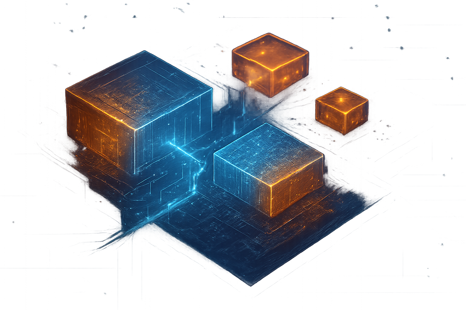
    The Architecture of Intelligence: Unpacking Specialized AI Chip Advancements

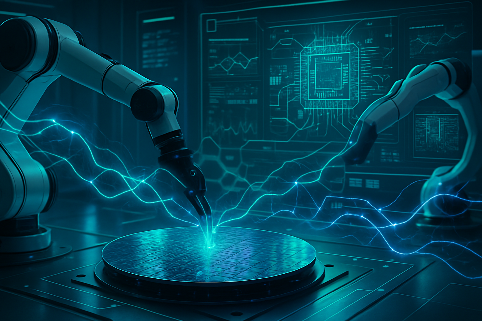
    The current wave of AI advancements, particularly in deep learning and large language models, demands computational power far beyond the capabilities of general-purpose CPUs. This has spurred the development and refinement of specialized AI chips, each optimized for specific aspects of AI workloads.

    Graphics Processing Units (GPUs), initially designed for rendering complex graphics, have become the workhorse of AI training due to their highly parallel architectures. Companies like NVIDIA Corporation (NASDAQ: NVDA) have capitalized on this, transforming their GPUs into the de facto standard for deep learning. Their latest architectures, such as Hopper and Blackwell, feature thousands of CUDA cores and Tensor Cores specifically designed for matrix multiplication operations crucial for neural networks. The Blackwell platform, for instance, boasts a 20 PetaFLOPS FP8 AI engine and 8TB/s bidirectional interconnect, significantly accelerating both training and inference tasks compared to previous generations. This parallel processing capability allows GPUs to handle the massive datasets and complex calculations involved in training sophisticated AI models far more efficiently than traditional CPUs, which are optimized for sequential processing.

    Beyond GPUs, Application-Specific Integrated Circuits (ASICs) represent the pinnacle of optimization for particular AI tasks. Alphabet Inc.'s (NASDAQ: GOOGL) Tensor Processing Units (TPUs) are a prime example. Designed specifically for Google's TensorFlow framework, TPUs offer superior performance and energy efficiency for specific AI workloads, particularly inference in data centers. Each generation of TPUs brings enhanced matrix multiplication capabilities and increased memory bandwidth, tailoring the hardware precisely to the software's needs. This specialization allows ASICs to outperform more general-purpose chips for their intended applications, albeit at the cost of flexibility.

    Field-Programmable Gate Arrays (FPGAs) offer a middle ground, providing reconfigurability that allows them to be adapted for different AI models or algorithms post-manufacturing. While not as performant as ASICs for a fixed task, their flexibility makes them valuable for rapid prototyping and for inference tasks where workloads might change. Xilinx (now AMD) (NASDAQ: AMD) has been a key player in this space, offering adaptive computing platforms that can be programmed for various AI acceleration tasks.

    The technical specifications of these chips include increasingly higher transistor counts, advanced packaging technologies like 3D stacking (e.g., High-Bandwidth Memory – HBM), and specialized instruction sets for AI operations. These innovations represent a departure from the "general-purpose computing" paradigm, moving towards "domain-specific architectures" where hardware is meticulously crafted to excel at AI tasks. Initial reactions from the AI research community and industry experts have been overwhelmingly positive, acknowledging that these specialized chips are not just enabling current AI breakthroughs but are foundational to the next generation of intelligent systems, though concerns about their cost, power consumption, and accessibility persist.

    Corporate Chessboard: AI Chips Reshaping the Tech Landscape

    The escalating demand for specialized AI chips is profoundly reshaping the competitive dynamics within the tech industry, creating clear beneficiaries, intensifying rivalries, and driving strategic shifts among major players and startups alike.

    NVIDIA Corporation (NASDAQ: NVDA) stands as the undeniable titan in this new era, having established an early and dominant lead in the AI chip market, particularly with its GPUs. Their CUDA platform, a proprietary parallel computing platform and programming model, has fostered a vast ecosystem of developers and applications, creating a significant moat. This market dominance has translated into unprecedented financial growth, with their GPUs becoming the gold standard for AI training in data centers. The company's strategic advantage lies not just in hardware but in its comprehensive software stack, making it challenging for competitors to replicate its end-to-end solution.

    However, this lucrative market has attracted fierce competition. Intel Corporation (NASDAQ: INTC), traditionally a CPU powerhouse, is aggressively pursuing the AI chip market with its Gaudi accelerators (from Habana Labs acquisition) and its own GPU initiatives like Ponte Vecchio. Intel's vast manufacturing capabilities and established relationships within the enterprise market position it as a formidable challenger. Similarly, Advanced Micro Devices, Inc. (NASDAQ: AMD) is making significant strides with its Instinct MI series GPUs, aiming to capture a larger share of the data center AI market by offering competitive performance and a more open software ecosystem.

    Tech giants like Alphabet Inc. (NASDAQ: GOOGL) and Amazon.com, Inc. (NASDAQ: AMZN) are also investing heavily in developing their own custom AI ASICs. Google's TPUs power its internal AI infrastructure and are offered through Google Cloud, providing a highly optimized solution for its services. Amazon's AWS division has developed custom chips like Inferentia and Trainium to power its machine learning services, aiming to reduce costs and optimize performance for its cloud customers. This in-house chip development strategy allows these companies to tailor hardware precisely to their software needs, potentially reducing reliance on external vendors and gaining a competitive edge in cloud AI services.

    For startups, the landscape presents both opportunities and challenges. While the high cost of advanced chip design and manufacturing can be a barrier, there's a burgeoning ecosystem of startups focusing on niche AI accelerators, specialized architectures for edge AI, or innovative software layers that optimize performance on existing hardware. The competitive implications are clear: companies that can efficiently develop, produce, and deploy high-performance, energy-efficient AI chips will gain significant strategic advantages in the rapidly evolving AI market. This could lead to further consolidation or strategic partnerships as companies seek to secure their supply chains and technological leadership.

    Broadening Horizons: The Wider Significance of AI Chip Innovation

    The explosion in AI chip demand and innovation is not merely a technical footnote; it represents a pivotal shift with profound wider significance for the entire AI landscape, society, and global geopolitics. This specialization of hardware is fundamentally altering how AI is developed, deployed, and perceived, moving beyond theoretical advancements to tangible, widespread applications.

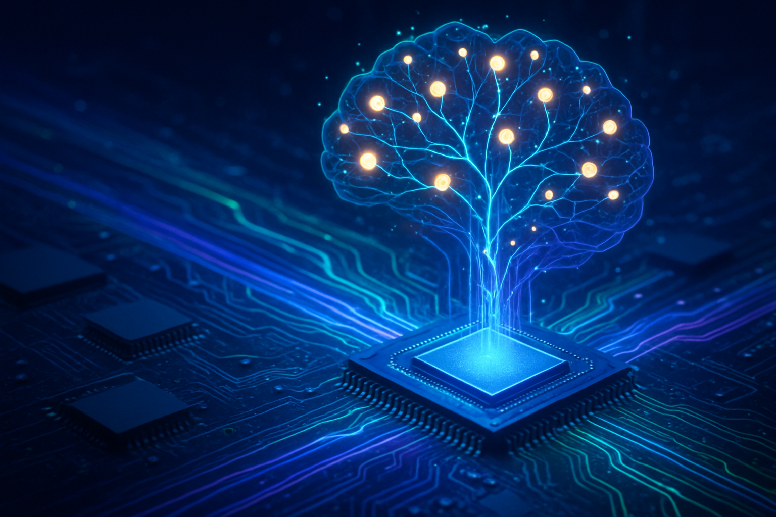
    Firstly, this trend underscores the increasing maturity of AI as a field. No longer confined to academic labs, AI is now a critical component of enterprise infrastructure, consumer products, and national security. The need for dedicated hardware signifies that AI is graduating from a software-centric discipline to one where hardware-software co-design is paramount for achieving breakthroughs in performance and efficiency. This fits into the broader AI landscape by enabling models of unprecedented scale and complexity, such as large language models, which would be computationally infeasible without specialized silicon.

    The impacts are far-reaching. On the positive side, more powerful and efficient AI chips will accelerate progress in areas like drug discovery, climate modeling, autonomous systems, and personalized medicine, leading to innovations that can address some of humanity's most pressing challenges. The integration of NPUs into everyday devices will bring sophisticated AI capabilities to the edge, enabling real-time processing and enhancing privacy by reducing the need to send data to the cloud.

    However, potential concerns also loom large. The immense energy consumption of training large AI models on these powerful chips raises significant environmental questions. The "AI energy footprint" is a growing area of scrutiny, pushing for innovations in energy-efficient chip design and sustainable data center operations. Furthermore, the concentration of advanced chip manufacturing capabilities in a few geographical regions, particularly Taiwan, has amplified geopolitical tensions. This has led to national initiatives, such as the CHIPS Act in the US and similar efforts in Europe, aimed at boosting domestic semiconductor production and reducing supply chain vulnerabilities, creating a complex interplay between technology, economics, and international relations.

    Comparisons to previous AI milestones reveal a distinct pattern. While earlier breakthroughs like expert systems or symbolic AI focused more on algorithms and logic, the current era of deep learning and neural networks is intrinsically linked to hardware capabilities. The development of specialized AI chips mirrors the shift from general-purpose computing to accelerated computing, akin to how GPUs revolutionized scientific computing. This signifies that hardware limitations, once a bottleneck, are now actively being addressed and overcome, paving the way for AI to permeate every facet of our digital and physical worlds.

    The Road Ahead: Future Developments in AI Chip Technology

    The trajectory of AI chip innovation points towards a future characterized by even greater specialization, energy efficiency, and novel computing paradigms, addressing both current limitations and enabling entirely new applications.

    In the near term, we can expect continued refinement of existing architectures. This includes further advancements in GPU designs, pushing the boundaries of parallel processing, memory bandwidth, and interconnect speeds. ASICs will become even more optimized for specific AI tasks, with companies developing custom silicon for everything from advanced robotics to personalized AI assistants. A significant trend will be the deeper integration of AI accelerators directly into CPUs and SoCs, making AI processing ubiquitous across a wider range of devices, from high-end servers to low-power edge devices. This "AI everywhere" approach will likely see NPUs becoming standard components in next-generation smartphones, laptops, and IoT devices.

    Long-term developments are poised to be even more transformative. Researchers are actively exploring neuromorphic computing, which aims to mimic the structure and function of the human brain. Chips based on neuromorphic principles, such as Intel's Loihi and IBM's TrueNorth, promise ultra-low power consumption and highly efficient processing for certain AI tasks, potentially unlocking new frontiers in cognitive AI. Quantum computing also holds the promise of revolutionizing AI by tackling problems currently intractable for classical computers, though its widespread application for AI is still further down the road. Furthermore, advancements in materials science, such as 2D materials and carbon nanotubes, could lead to chips that are smaller, faster, and more energy-efficient than current silicon-based technologies.

    Challenges that need to be addressed include the aforementioned energy consumption concerns, requiring breakthroughs in power management and cooling solutions. The complexity of designing and manufacturing these advanced chips will continue to rise, necessitating sophisticated AI-driven design tools and advanced fabrication techniques. Supply chain resilience will remain a critical focus, with efforts to diversify manufacturing geographically. Experts predict a future where AI chips are not just faster, but also smarter, capable of learning and adapting on-chip, and seamlessly integrated into a vast, intelligent ecosystem.

    The Silicon Brain: A New Chapter in AI History

    The rapid growth of AI has ignited an unprecedented revolution in the semiconductor sector, marking a pivotal moment in the history of artificial intelligence. The insatiable demand for specialized AI chips – from powerful GPUs and custom ASICs to versatile FPGAs and integrated NPUs – underscores a fundamental shift in how we approach and enable intelligent machines. This era is defined by a relentless pursuit of computational efficiency and performance, with hardware innovation now intrinsically linked to the progress of AI itself.

    Key takeaways from this dynamic landscape include the emergence of domain-specific architectures as the new frontier of computing, the intense competitive race among tech giants and chipmakers, and the profound implications for global supply chains and geopolitical stability. This development signifies that AI is no longer a nascent technology but a mature and critical infrastructure component, demanding dedicated, highly optimized hardware to unlock its full potential.

    Looking ahead, the long-term impact of this chip innovation will be transformative, enabling AI to permeate every aspect of our lives, from highly personalized digital experiences to groundbreaking scientific discoveries. The challenges of energy consumption, manufacturing complexity, and talent shortages remain, but the ongoing research into neuromorphic computing and advanced materials promises solutions that will continue to push the boundaries of what's possible. As AI continues its exponential ascent, the semiconductor industry will remain at its heart, constantly evolving to build the silicon brains that power the intelligent future. We must watch for continued breakthroughs in chip architectures, the diversification of manufacturing capabilities, and the integration of AI accelerators into an ever-wider array of devices in the coming weeks and months.

    This content is intended for informational purposes only and represents analysis of current AI developments.
    TokenRing AI delivers enterprise-grade solutions for multi-agent AI workflow orchestration, AI-powered development tools, and seamless remote collaboration platforms.
    For more information, visit https://www.tokenring.ai/.

  • Stripe Unleashes Agentic AI to Revolutionize Payments, Ushering in a New Era of Autonomous Commerce

    Stripe Unleashes Agentic AI to Revolutionize Payments, Ushering in a New Era of Autonomous Commerce

    New York, NY – October 2, 2025 – Stripe, a leading financial infrastructure platform, has ignited a transformative shift in digital commerce with its aggressive push into agentic artificial intelligence for payments. Announced on Monday, September 30, 2025, at its annual new product event, Stripe unveiled a comprehensive suite of AI-powered innovations, including the groundbreaking Agentic Commerce Protocol (ACP) and a partnership with OpenAI (OTC: OPNAI) to power "Instant Checkout" within ChatGPT. This strategic move positions Stripe as a foundational layer for the burgeoning "Agent Economy," where AI agents will autonomously facilitate transactions, fundamentally reshaping how businesses sell and consumers buy online.

    The immediate significance of this development is profound. Stripe is not merely enhancing existing payment systems; it is actively building the economic rails for a future where AI agents become active participants in commercial transactions. This creates a revolutionary new commerce modality, allowing consumers to complete purchases directly within conversational AI interfaces, moving seamlessly from product discovery to transaction. Analysts project AI-driven commerce could swell to a staggering $1.7 trillion by 2030, and Stripe is vying to be at the heart of this explosive growth, setting the stage for an intense competitive race among tech and payment giants to dominate this nascent market.

    The Technical Backbone of Autonomous Transactions

    Stripe's foray into agentic AI is underpinned by sophisticated technical advancements designed to enable secure, seamless, and standardized AI-driven commerce. The core components include the Agentic Commerce Protocol (ACP), Instant Checkout in ChatGPT, and the innovative Shared Payment Token (SPT).

    The Agentic Commerce Protocol (ACP), co-developed by Stripe and OpenAI, is an open-source specification released under the Apache 2.0 license. It functions as a "shared language" for AI agents and businesses to communicate order details and payment instructions programmatically. Unlike proprietary systems, ACP allows any business or AI agent to implement it, fostering broad adoption beyond Stripe's ecosystem. Crucially, ACP emphasizes merchant sovereignty, ensuring businesses retain full control over their product listings, pricing, branding, fulfillment, and customer relationships, even as AI agents facilitate sales. Its flexible design supports various commerce types, from physical goods to subscriptions, and aims to accommodate custom checkout capabilities.

    Instant Checkout in ChatGPT is the flagship application demonstrating ACP's capabilities. This feature allows ChatGPT users to complete purchases directly within the chat interface. For instance, a user asking for product recommendations can click a "buy" button that appears, confirm order details, and complete the purchase, all without leaving the conversation. ChatGPT acts as the buyer's AI agent, securely relaying information between the user and the merchant. Initially supporting single-item purchases from US-based Etsy (NASDAQ: ETSY) sellers, Stripe plans a rapid expansion to over a million Shopify (NYSE: SHOP) merchants, including major brands like Glossier, Vuori, Spanx, and SKIMS.

    Central to the security and functionality of this new paradigm is the Shared Payment Token (SPT). This new payment primitive, issued by Stripe, allows AI applications to initiate payments without directly handling or exposing sensitive buyer payment credentials (like credit card numbers). SPTs are highly scoped, restricted to a specific merchant, cart total, and have defined usage limits and expiry windows. This significantly enhances security and reduces the PCI DSS (Payment Card Industry Data Security Standard) compliance burden for both the AI agent and the merchant. When a buyer confirms a purchase in the AI interface, Stripe issues the SPT, which ChatGPT then passes to the merchant via an API for processing.

    These technologies represent a fundamental departure from previous e-commerce models. Traditional online shopping is human-driven, requiring manual navigation and input. Agentic commerce, conversely, is built for AI agents acting on behalf of the buyer, embedding transactional capabilities directly within conversational AI. This eliminates redirects, streamlines the user journey, and offers a novel level of security through scoped SPTs. Initial reactions from the AI research community and industry experts have been largely enthusiastic, with many calling it a "revolutionary shift" and "the biggest development in commerce" in recent years. However, some express concerns about the potential for AI platforms to become "mandatory middlemen," raising questions about neutrality and platform pressure for merchants to integrate with numerous AI shopping portals.

    Reshaping the Competitive Landscape

    Stripe's aggressive push into agentic AI carries significant competitive implications for a wide array of players, from burgeoning AI startups to established tech giants and payment behemoths. This move signals a strategic intent to become the "economic infrastructure for AI," redefining financial interactions in an AI-driven world.

    Companies currently utilizing Stripe, particularly Etsy (NASDAQ: ETSY) and Shopify (NYSE: SHOP) merchants, stand to benefit immediately. The Instant Checkout feature in ChatGPT provides a new, frictionless sales channel, potentially boosting conversion rates by allowing purchases directly within AI conversations. More broadly, e-commerce and SaaS businesses leveraging Stripe will see enhanced operational efficiencies through improved payment accuracy, reduced fraud risks via Stripe Radar's AI models, and streamlined financial workflows. Stripe's suite of AI monetization tools, including flexible billing for hybrid revenue models and real-time LLM cost tracking, also makes it an attractive partner for AI companies and startups like Anthropic and Perplexity, helping them monetize their offerings and accelerate growth.

    The competitive landscape for major AI labs is heating up. OpenAI (OTC: OPNAI), as a co-developer of ACP and partner for Instant Checkout, gains a significant advantage by integrating commerce capabilities directly into its leading AI, potentially rivaling traditional e-commerce platforms. However, this also pits Stripe against other tech giants. Google (NASDAQ: GOOGL), for instance, has introduced its own competing Agent Payments Protocol (AP2), indicating a clear race to establish the default infrastructure for AI-native commerce. While Google Pay is an accepted payment method within OpenAI's Instant Checkout, it underscores a complex interplay of competition and collaboration. Similarly, Apple (NASDAQ: AAPL) Pay is also supported, but Apple has yet to fully embed its payment solution into agentic commerce flows, presenting both a challenge and an opportunity. Amazon (NASDAQ: AMZN), with its traditional e-commerce dominance, faces disruption as AI agents can autonomously shop across various platforms, prompting Amazon to explore its own "Buy for Me" features.

    For established payment giants like Visa (NYSE: V) and Mastercard (NYSE: MA), Stripe's move represents a direct challenge and a call to action. Both companies are actively developing their own "agentic AI commerce" solutions, such as Visa Intelligent Commerce and Mastercard Agent Pay, leveraging existing tokenization infrastructure to secure AI-driven transactions. The strategic race is not merely about who processes payments fastest, but who becomes the default "rail" for AI-native commerce. Stripe's expansion into stablecoin issuance also directly competes with traditional banks and cross-border payment providers, offering businesses programmable money capabilities.

    This disruption extends to various existing products and services. Traditional payment gateways, less integrated with AI, may struggle to compete. Stripe Radar's AI-driven fraud detection, leveraging data from trillions of dollars in transactions, could render legacy fraud methods obsolete. The shift from human-driven browsing to AI-driven delegation fundamentally changes the e-commerce user experience, moving beyond traditional search and click-through models. Stripe's early-mover advantage, deep data and AI expertise from its Payments Foundation Model, developer-first ecosystem, and comprehensive AI monetization tools provide it with a strong market positioning, aiming to become the default payment layer for the "Agent Economy."

    A New Frontier in the AI Landscape

    Stripe's push into agentic AI for payments is not merely an incremental improvement; it signifies a pivotal moment in the broader AI landscape, marking a decisive shift from reactive or generative AI to truly autonomous, goal-oriented systems. This initiative positions agentic AI as the next frontier in automation, capable of perceiving, reasoning, acting, and learning without constant human intervention.

    Historically, AI has evolved through several stages: from early rule-based expert systems to machine learning that enabled predictions from data, and more recently, to deep learning and generative AI that can create human-like content. Agentic AI leverages these advancements but extends them to autonomous action and multi-step goal achievement in real-world domains. Stripe's Agentic Commerce Protocol (ACP) embodies this by providing the open standard for AI agents to manage complex transactions. This transforms AI from a powerful tool into an active participant in economic processes, redefining how commerce is conducted and establishing a new paradigm where AI agents are integral to buying and selling. It's seen as a "new era" for financial services, promising to redefine financial operations by moving from analytical or generative capabilities to proactive, autonomous execution.

    The wider societal and economic impacts are multifaceted. On the positive side, agentic AI promises enhanced efficiency and cost reduction through automated tasks like fraud detection, regulatory compliance, and customer support. It can lead to hyper-personalized financial services, improved fraud detection and risk management, and potentially greater financial inclusion by autonomously assessing micro-loans or personalized micro-insurance. For commerce, it enables revolutionary shifts, turning AI-driven discovery into direct sales channels.

    However, significant concerns accompany this technological leap. Data privacy is paramount, as agentic AI systems rely on extensive personal and behavioral data. Risks include over-collection of Personally Identifiable Information (PII), data leakage, and vulnerabilities related to third-party data sharing, necessitating strict adherence to regulations like GDPR and CCPA. Ethical AI use is another critical area. Algorithmic bias, if trained on skewed datasets, could perpetuate discrimination in financial decisions. The "black box" nature of many advanced AI models raises issues of transparency and explainability (XAI), making it difficult to understand decision-making processes and undermining trust. Furthermore, accountability becomes a complex legal and ethical challenge when autonomous AI systems make flawed or harmful decisions. Responsible deployment demands fairness-aware machine learning, regular audits, diverse datasets, and "compliance by design."

    Finally, the potential for job displacement is a significant societal concern. While AI is expected to automate routine tasks in the financial sector, potentially leading to job reductions in roles like data entry and loan processing, this transformation is also anticipated to reshape existing jobs and create new ones, requiring reskilling in areas like AI interpretation and strategic decision-making. Goldman Sachs (NYSE: GS) suggests the overall impact on employment levels may be modest and temporary, with new job opportunities emerging.

    The Horizon of Agentic Commerce

    The future of Stripe's agentic AI in payments promises rapid evolution, marked by both near-term enhancements and long-term transformative developments. Experts predict a staged maturity curve for agentic commerce, beginning with initial "discovery bots" and gradually progressing towards fully autonomous transaction capabilities.

    In the near-term (2025-2027), Stripe plans to expand its Payments Foundation Model across more products, further enhancing fraud detection, authorization rates, and overall payment performance. The Agentic Commerce Protocol (ACP) will see wider adoption beyond its initial OpenAI (OTC: OPNAI) integration, as Stripe collaborates with other AI companies like Anthropic and Microsoft (NASDAQ: MSFT) Copilot. The Instant Checkout feature is expected to rapidly expand its merchant and geographic coverage beyond Etsy (NASDAQ: ETSY) and Shopify (NYSE: SHOP) in the US. Stripe will also continue to roll out AI-powered optimizations across its entire payment lifecycle, from personalized checkout experiences to advanced fraud prevention with Radar for platforms.

    Looking long-term (beyond 2027), experts anticipate the achievement of full autonomy in complex workflows for agentic commerce by 2030. Stripe envisions stablecoins and AI behaviors becoming deeply integrated into the payments stack, moving beyond niche experiments to foundational rails for digital transactions. This necessitates a re-architecting of commerce systems, from payments and checkout to fraud checks, preparing for a new paradigm where bots operate seamlessly between consumers and businesses. AI engines themselves are expected to seek new revenue streams as agentic commerce becomes inevitable, driving the adoption of "a-commerce."

    Potential future applications and use cases are vast. AI agents will enable autonomous shopping and procurement, not just for consumers restocking household items, but also for B2B buyers managing complex procurement flows. This includes searching options, comparing prices, filling carts, and managing orders. Hyper-personalized experiences will redefine commerce, offering tailored payment options and product recommendations based on individual preferences. AI will further enhance fraud detection and prevention, provide optimized payment routing, and revolutionize customer service and marketing automation through 1:1 experiences and advanced targeting. The integration with stablecoins is also a key area, as Stripe explores issuing bespoke stablecoins and facilitating their transaction via AI agents, leveraging their 24/7 operation and global reach for efficient settlement.

    Despite the immense potential, several challenges must be addressed for widespread adoption. A significant consumer trust gap exists, with only a quarter of US consumers currently comfortable letting AI make purchases today. Enterprise hesitation mirrors this sentiment. Data privacy concerns remain paramount, requiring robust measures beyond basic anonymization. Security and governance risks associated with autonomous agents, including the challenge of differentiating "good bots" from "bad bots" in fraud models, demand continuous innovation. Furthermore, interoperability and infrastructure are crucial; fintechs and neobanks will need to create new systems to ensure seamless integration with agent-initiated payments, as traditional checkout flows are often not designed for AI. The emergence of competing protocols, such as Google's (NASDAQ: GOOGL) AP2 alongside Stripe's ACP, also highlights the challenge of establishing a truly universal open standard. Experts predict a fundamental shift from human browsing to delegating purchases to AI agents, with AI chatbots becoming the new storefronts and user interfaces. Brands must adapt to "Answer Engine Optimization (AEO)" to remain discoverable by these AI agents.

    A Defining Moment for AI and Commerce

    Stripe's ambitious foray into agentic AI for payments marks a defining moment in the history of artificial intelligence and digital commerce. It represents a significant leap beyond previous AI paradigms, moving from predictive and generative capabilities to autonomous, proactive execution of real-world economic actions. By introducing the Agentic Commerce Protocol (ACP), powering Instant Checkout in ChatGPT, and leveraging its advanced Payments Foundation Model, Stripe is not just adapting to the future; it is actively building the foundational infrastructure for the "Agent Economy."

    The key takeaways from this development underscore Stripe's strategic vision: establishing an open standard for AI-driven transactions, seamlessly integrating commerce into conversational AI, and providing a robust, AI-powered toolkit for businesses to optimize their entire payment lifecycle. This move positions Stripe as a central player in a rapidly evolving landscape, offering unprecedented efficiency, personalization, and security in financial transactions.

    The long-term impact on the tech industry and society will be profound. Agentic commerce is poised to revolutionize digital sales, creating new revenue streams for businesses and transforming the consumer shopping experience. While ushering in an era of unparalleled convenience, it also necessitates careful consideration of critical issues such as data privacy, algorithmic bias, and accountability in autonomous systems. The competitive "arms race" among payment processors and tech giants to become the default rail for AI-native commerce will intensify, driving further innovation and potentially consolidating power among early movers. The parallel rise of programmable money, particularly stablecoins, further integrates with this vision, offering a 24/7, efficient settlement layer for AI-driven transactions.

    In the coming weeks and months, the tech world will be closely watching several key indicators. The pace of ACP adoption by other AI agents and platforms, beyond ChatGPT, will be crucial. The expansion of Instant Checkout to a broader range of merchants and geographies will demonstrate its real-world viability and impact. Responses from competitors, including new partnerships and competing protocols, will shape the future landscape of agentic commerce. Furthermore, developments in security, trust-building mechanisms, and emerging regulatory frameworks for autonomous financial transactions will be paramount for widespread adoption. As Stripe continues to leverage its unique data insights from "intent, interaction, and transaction," expect further innovations in payment optimization and personalized commerce, potentially giving rise to entirely new business models. This is not just about payments; it's about the very fabric of future economic interaction.

    This content is intended for informational purposes only and represents analysis of current AI developments.

    TokenRing AI delivers enterprise-grade solutions for multi-agent AI workflow orchestration, AI-powered development tools, and seamless remote collaboration platforms.
    For more information, visit https://www.tokenring.ai/.

  • Beyond Moore’s Law: Chiplets and Heterogeneous Integration Reshape the Future of Semiconductor Performance

    Beyond Moore’s Law: Chiplets and Heterogeneous Integration Reshape the Future of Semiconductor Performance

    The semiconductor industry is undergoing its most significant architectural transformation in decades, moving beyond the traditional monolithic chip design to embrace a modular future driven by chiplets and heterogeneous integration. This paradigm shift is not merely an incremental improvement but a fundamental re-imagining of how high-performance computing, artificial intelligence, and next-generation devices will be built. As the physical and economic limits of Moore's Law become increasingly apparent, chiplets and heterogeneous integration offer a critical pathway to continue advancing performance, power efficiency, and functionality, heralding a new era of innovation in silicon.

    This architectural evolution is particularly significant as it addresses the escalating challenges of fabricating increasingly complex and larger chips on a single silicon die. By breaking down intricate functionalities into smaller, specialized "chiplets" and then integrating them into a single package, manufacturers can achieve unprecedented levels of customization, yield improvements, and performance gains. This strategy is poised to unlock new capabilities across a vast array of applications, from cutting-edge AI accelerators to robust data center infrastructure and advanced mobile platforms, fundamentally altering the competitive landscape for chip designers and technology giants alike.

    A Modular Revolution: Unpacking the Technical Core of Chiplet Design

    At its heart, the rise of chiplets represents a departure from the monolithic System-on-Chip (SoC) design, where all functionalities—CPU cores, GPU, memory controllers, I/O—are squeezed onto a single piece of silicon. While effective for decades, this approach faces severe limitations as transistor sizes shrink and designs grow more complex, leading to diminishing returns in terms of cost, yield, and power. Chiplets, in contrast, are smaller, self-contained functional blocks, each optimized for a specific task (e.g., a CPU core, a GPU tile, a memory controller, an I/O hub).

    The true power of chiplets is unleashed through heterogeneous integration (HI), which involves assembling these diverse chiplets—often manufactured using different, optimal process technologies—into a single, advanced package. This integration can take various forms, including 2.5D integration (where chiplets are placed side-by-side on an interposer, effectively a silicon bridge) and 3D integration (where chiplets are stacked vertically, connected by through-silicon vias, or TSVs). This multi-die approach allows for several critical advantages:

    • Improved Yield and Cost Efficiency: Manufacturing smaller chiplets significantly increases the likelihood of producing defect-free dies, boosting overall yield. This allows for the use of advanced, more expensive process nodes only for the most performance-critical chiplets, while other components can be fabricated on more mature, cost-effective nodes.
    • Enhanced Performance and Power Efficiency: By allowing each chiplet to be designed and fabricated with the most suitable process technology for its function, overall system performance can be optimized. The close proximity of chiplets within advanced packages, facilitated by high-bandwidth, low-latency interconnects, dramatically reduces signal travel time and power consumption compared to traditional board-level interconnections.
    • Greater Scalability and Customization: Chiplets enable a "lego-block" approach to chip design. Designers can mix and match various chiplets to create highly customized solutions tailored to specific performance, power, and cost requirements for diverse applications, from high-performance computing (HPC) to edge AI.
    • Overcoming Reticle Limits: Monolithic designs are constrained by the physical size limits of lithography reticles. Chiplets bypass this by distributing functionality across multiple smaller dies, allowing for the creation of systems far larger and more complex than a single, monolithic chip could achieve.

    Initial reactions from the AI research community and industry experts have been overwhelmingly positive, recognizing chiplets and heterogeneous integration as the definitive path forward for scaling performance in the post-Moore's Law era. The establishment of industry standards like the Universal Chiplet Interconnect Express (UCIe), backed by major players, further solidifies this shift, ensuring interoperability and fostering a robust ecosystem for chiplet-based designs. This collaborative effort is crucial for enabling a future where chiplets from different vendors can seamlessly communicate within a single package, driving innovation and competition.

    Reshaping the Competitive Landscape: Strategic Implications for Tech Giants and Startups

    The strategic implications of chiplets and heterogeneous integration are profound, fundamentally reshaping the competitive dynamics across the AI and semiconductor industries. This modular approach empowers certain players, disrupts traditional market structures, and creates new avenues for innovation, particularly for those at the forefront of AI development.

    Advanced Micro Devices (NASDAQ: AMD) stands out as a pioneer and significant beneficiary of this architectural shift. Having embraced chiplets in its Ryzen and EPYC processors since 2017/2019, and more recently in its Instinct MI300A and MI300X AI accelerators, AMD has demonstrated the cost-effectiveness and flexibility of the approach. By integrating CPU, GPU, FPGA, and high-bandwidth memory (HBM) chiplets onto a single substrate, AMD can offer highly customized and scalable solutions for a wide range of AI workloads, providing a strong competitive alternative to NVIDIA in segments like large language model inference. This strategy has allowed AMD to achieve higher yields and lower marginal costs, bolstering its market position.

    Intel Corporation (NASDAQ: INTC) is also heavily invested in chiplet technology through its ambitious IDM 2.0 strategy. Leveraging advanced packaging technologies like Foveros and EMIB, Intel is deploying multiple "tiles" (chiplets) in its Meteor Lake and upcoming Arrow Lake processors for different functions. This allows for CPU and GPU performance scaling by upgrading or swapping individual chiplets rather than redesigning an entire monolithic processor. Intel's Programmable Solutions Group (PSG) has utilized chiplets in its Agilex FPGAs since 2016, and the company is actively fostering a broader ecosystem through its "Chiplet Alliance" with industry leaders like Ansys, Arm, Cadence, Siemens, and Synopsys. A notable partnership with NVIDIA Corporation (NASDAQ: NVDA) to build x86 SoCs integrating NVIDIA RTX GPU chiplets for personal computing further underscores this collaborative and modular future.

    While NVIDIA has historically focused on maximizing performance through monolithic designs for its high-end GPUs, the company is also making a strategic pivot. Its Blackwell platform, featuring the B200 chip with two chiplets for its 208 billion transistors, marks a significant step towards a chiplet-based future. As lithographic limits are reached, even NVIDIA, the dominant force in AI acceleration, recognizes the necessity of chiplets to continue pushing performance boundaries, exploring designs with specialized accelerator chiplets for different workloads.

    Beyond traditional chipmakers, hyperscalers like Alphabet Inc. (NASDAQ: GOOGL) (Google), Amazon.com, Inc. (NASDAQ: AMZN) (AWS), and Microsoft Corporation (NASDAQ: MSFT) are making substantial investments in designing their own custom AI chips. Google's Tensor Processing Units (TPUs), Amazon's Graviton, Inferentia, and Trainium chips, and Microsoft's custom AI silicon all leverage heterogeneous integration to optimize for their specific cloud workloads. This vertical integration allows these tech giants to tightly optimize hardware with their software stacks and cloud infrastructure, reducing reliance on external suppliers and offering improved price-performance and lower latency for their machine learning services.

    The competitive landscape is further shaped by the critical role of foundry and packaging providers like Taiwan Semiconductor Manufacturing Company (NYSE: TSM) (TSMC) with its CoWoS technology, and Intel Foundry Services (IFS) with EMIB/Foveros. These companies provide the advanced manufacturing capabilities and packaging technologies essential for heterogeneous integration. Electronic Design Automation (EDA) companies such as Synopsys, Cadence, and Ansys are also indispensable, offering the tools required to design and verify these complex multi-die systems. For startups, chiplets present both immense opportunities and challenges. While the high cost of advanced packaging and access to cutting-edge fabs remain hurdles, chiplets lower the barrier to entry for designing specialized silicon. Startups can now focus on creating highly optimized chiplets for niche AI functions or developing innovative interconnect technologies, fostering a vibrant ecosystem of specialized IP and accelerating hardware development cycles for specific, smaller volume applications without the prohibitive costs of a full monolithic SoC.

    A Foundational Shift for AI: Broader Significance and Historical Parallels

    The architectural revolution driven by chiplets and heterogeneous integration extends far beyond mere silicon manufacturing; it represents a foundational shift that will profoundly influence the trajectory of Artificial Intelligence. This paradigm is crucial for sustaining the rapid pace of AI innovation in an era where traditional scaling benefits are diminishing, echoing and, in some ways, surpassing the impact of previous hardware breakthroughs.

    This development squarely addresses the challenges of the "More than Moore" era. For decades, AI progress was intrinsically linked to Moore's Law—the relentless doubling of transistors on a chip. As physical limits are reached, chiplets offer an alternative pathway to performance gains, focusing on advanced packaging and integration rather than solely on transistor density. This redefines how computational power is achieved, moving from monolithic scaling to modular optimization. The ability to integrate diverse functionalities—compute, memory, I/O, and even specialized AI accelerators—into a single package with high-bandwidth, low-latency interconnects directly tackles the "memory wall" problem, a critical bottleneck for data-intensive AI workloads by saving significant I/O power and boosting throughput.

    The significance of chiplets for AI can be compared to the GPU revolution of the mid-2000s. Originally designed for graphics rendering, GPUs proved exceptionally adept at the parallel computations required for neural network training, catalyzing the deep learning boom. Similarly, the rise of specialized AI accelerators like Google's (NASDAQ: GOOGL) Tensor Processing Units (TPUs) further optimized hardware for specific deep learning tasks. Chiplets extend this trend by enabling even finer-grained specialization. Instead of a single, large AI accelerator, multiple specialized AI chiplets can be combined, each tailored for different aspects or layers of a neural network (e.g., convolution, activation, attention mechanisms). This allows for a bespoke approach to AI hardware, providing unparalleled customization and efficiency for increasingly complex and diverse AI models.

    However, this transformative shift is not without its challenges. Standardization remains a critical concern; while initiatives like the Universal Chiplet Interconnect Express (UCIe) aim to foster interoperability, proprietary die-to-die interconnects still complicate a truly open chiplet ecosystem. The design complexity of optimizing power, thermal efficiency, and routing in multi-die architectures demands advanced Electronic Design Automation (EDA) tools and co-design methodologies. Furthermore, manufacturing costs for advanced packaging, coupled with intricate thermal management and power delivery requirements for densely integrated systems, present significant engineering hurdles. Security also emerges as a new frontier of concern, with chiplet-based designs introducing potential vulnerabilities related to hardware Trojans, cross-die side-channel attacks, and intellectual property theft across a more distributed supply chain. Despite these challenges, the ability of chiplets to provide increased performance density, energy efficiency, and unparalleled customization makes them indispensable for the next generation of AI, particularly for the immense computational demands of large generative models and the diverse requirements of multimodal and agentic AI.

    The Road Ahead: Future Developments and the AI Horizon

    The trajectory of chiplets and heterogeneous integration points towards an increasingly modular and specialized future for computing, with profound implications for AI. This architectural shift is not a temporary trend but a long-term strategic direction for the semiconductor industry, promising continued innovation well beyond the traditional limits of silicon scaling.

    In the near-term (1-5 years), we can expect the widespread adoption of advanced packaging technologies like 2.5D and 3D hybrid bonding to become standard practice for high-performance AI and HPC systems. The Universal Chiplet Interconnect Express (UCIe) standard will solidify its position, facilitating greater interoperability and fostering a more open chiplet ecosystem. This will accelerate the development of truly modular AI systems, where specialized compute, memory, and I/O chiplets can be flexibly combined. Concurrently, significant advancements in power distribution networks (PDNs) and thermal management solutions will be crucial to handle the increasing integration density. Intriguingly, AI itself will play a pivotal role, with AI-driven design automation tools becoming indispensable for optimizing IC layout and achieving optimal power, performance, and area (PPA) in complex chiplet-based designs.

    Looking further into the long-term, the industry is poised for fully modular semiconductor designs, with custom chiplets optimized for specific AI workloads dominating future architectures. The transition from 2.5D to more prevalent 3D heterogeneous computing, featuring tightly integrated compute and memory stacks, will become commonplace, driven by Through-Silicon Vias (TSVs) and advanced hybrid bonding. A significant breakthrough will be the widespread integration of Co-Packaged Optics (CPO), directly embedding optical communication into packages. This will offer significantly higher bandwidth and lower transmission loss, effectively addressing the persistent "memory wall" challenge for data-intensive AI. Furthermore, the ability to integrate diverse and even incompatible semiconductor materials (e.g., GaN, SiC) will expand the functionality of chiplet-based systems, enabling novel applications.

    These developments will unlock a vast array of potential applications and use cases. For Artificial Intelligence (AI) and Machine Learning (ML), custom chiplets will be the bedrock for handling the escalating complexity of large language models (LLMs), computer vision, and autonomous driving, allowing for tailored configurations that optimize performance and energy efficiency. High-Performance Computing (HPC) will benefit from larger-scale integration and modular designs, enabling more powerful simulations and scientific research. Data centers and cloud computing will leverage chiplets for high-performance servers, network switches, and custom accelerators, addressing the insatiable demand for memory and compute. Even edge computing, 5G infrastructure, and advanced automotive systems will see innovations driven by the ability to create efficient, specialized designs for resource-constrained environments.

    However, the path forward is not without its challenges. Ensuring efficient, low-latency, and high-bandwidth interconnects between chiplets remains paramount, as different implementations can significantly impact power and performance. The full realization of a multi-vendor chiplet ecosystem hinges on the widespread adoption of robust standardization efforts like UCIe. The inherent design complexity of multi-die architectures demands continuous innovation in EDA tools and co-design methodologies. Persistent issues around power and thermal management, quality control, mechanical stress from heterogeneous materials, and the increased supply chain complexity with associated security risks will require ongoing research and engineering prowess.

    Despite these hurdles, expert predictions are overwhelmingly positive. Chiplets are seen as an inevitable evolution, poised to be found in almost all high-performance computing systems, crucial for reducing inter-chip communication power and achieving necessary memory bandwidth. They are revolutionizing AI hardware by driving the demand for specialized and efficient computing architectures, breaking the memory wall for generative AI, and accelerating innovation by enabling faster time-to-market through modular reuse. This paradigm shift fundamentally redefines how computing systems, especially for AI and HPC, are designed and manufactured, promising a future of modular, high-performance, and energy-efficient computing that continues to push the boundaries of what AI can achieve.

    The New Era of Silicon: A Comprehensive Wrap-up

    The ascent of chiplets and heterogeneous integration marks a definitive turning point in the semiconductor industry, fundamentally redefining how high-performance computing and artificial intelligence systems are conceived, designed, and manufactured. This architectural pivot is not merely an evolutionary step but a revolutionary leap, crucial for navigating the post-Moore's Law landscape and sustaining the relentless pace of AI innovation.

    Key Takeaways from this transformation are clear: the future of chip design is inherently modular, moving beyond monolithic structures to a "mix-and-match" strategy of specialized chiplets. This approach unlocks significant performance and power efficiency gains, vital for the ever-increasing demands of AI workloads, particularly large language models. Heterogeneous integration is paramount for AI, allowing the optimal combination of diverse compute types (CPU, GPU, AI accelerators) and high-bandwidth memory (HBM) within a single package. Crucially, advanced packaging has emerged as a core architectural component, no longer just a protective shell. While immensely promising, the path forward is lined with challenges, including establishing robust interoperability standards, managing design complexity, addressing thermal and power delivery hurdles, and securing an increasingly distributed supply chain.

    In the grand narrative of AI history, this development stands as a pivotal milestone, comparable in impact to the invention of the transistor or the advent of the GPU. It provides a viable pathway beyond Moore's Law, enabling continued performance scaling when traditional transistor shrinkage falters. Chiplets are indispensable for enabling HBM integration, effectively breaking the "memory wall" that has long constrained data-intensive AI. They facilitate the creation of highly specialized AI accelerators, optimizing for specific tasks with unparalleled efficiency, thereby fueling advancements in generative AI, autonomous systems, and edge computing. Moreover, by allowing for the reuse of validated IP and mixing process nodes, chiplets democratize access to high-performance AI hardware, fostering cost-effective innovation across the industry.

    Looking to the long-term impact, chiplet-based designs are poised to become the new standard for complex, high-performance computing systems, especially within the AI domain. This modularity will be critical for the continued scalability of AI, enabling the development of more powerful and efficient AI models previously thought unimaginable. AI itself will increasingly be leveraged for AI-driven design automation, optimizing chiplet layouts and accelerating production. This paradigm also lays the groundwork for new computing paradigms like quantum and neuromorphic computing, which will undoubtedly leverage specialized computational units. Ultimately, this shift fosters a more collaborative semiconductor ecosystem, driven by open standards and a burgeoning "chiplet marketplace."

    In the coming weeks and months, several key indicators will signal the maturity and direction of this revolution. Watch closely for standardization progress from consortia like UCIe, as widespread adoption of interoperability standards is crucial. Keep an eye on advanced packaging innovations, particularly in hybrid bonding and co-packaged optics, which will push the boundaries of integration. Observe the growth of the ecosystem and new collaborations among semiconductor giants, foundries, and IP vendors. The maturation and widespread adoption of AI-assisted design tools will be vital. Finally, monitor how the industry addresses critical challenges in power, thermal management, and security, and anticipate new AI processor announcements from major players that increasingly showcase their chiplet-based and heterogeneously integrated architectures, demonstrating tangible performance and efficiency gains. The future of AI is modular, and the journey has just begun.

    This content is intended for informational purposes only and represents analysis of current AI developments.

    TokenRing AI delivers enterprise-grade solutions for multi-agent AI workflow orchestration, AI-powered development tools, and seamless remote collaboration platforms.
    For more information, visit https://www.tokenring.ai/.

  • AI Propels Silicon to Warp Speed: Chip Design Accelerated from Months to Minutes, Unlocking Unprecedented Innovation

    AI Propels Silicon to Warp Speed: Chip Design Accelerated from Months to Minutes, Unlocking Unprecedented Innovation

    Artificial intelligence (AI) is fundamentally transforming the semiconductor industry, marking a pivotal moment that goes beyond mere incremental improvements to represent a true paradigm shift in chip design and development. The immediate significance of AI-powered chip design tools stems from the escalating complexity of modern chip designs, the surging global demand for high-performance computing (HPC) and AI-specific chips, and the inability of traditional, manual methods to keep pace with these challenges. AI offers a potent solution, automating intricate tasks, optimizing critical parameters with unprecedented precision, and unearthing insights beyond human cognitive capacity, thereby redefining the very essence of hardware creation.

    This transformative impact is streamlining semiconductor development across multiple critical stages, drastically enhancing efficiency, quality, and speed. AI significantly reduces design time from months or weeks to days or even mere hours, as famously demonstrated by Google's efforts in optimizing chip placement. This acceleration is crucial for rapid innovation and getting products to market faster, pushing the boundaries of what is possible in silicon engineering.

    Technical Revolution: AI's Deep Dive into Chip Architecture

    AI's integration into chip design encompasses various machine learning techniques applied across the entire design flow, from high-level architectural exploration to physical implementation and verification. This paradigm shift offers substantial improvements over traditional Electronic Design Automation (EDA) tools.

    Reinforcement Learning (RL) agents, like those used in Google's AlphaChip, learn to make sequential decisions to optimize chip layouts for critical metrics such as Power, Performance, and Area (PPA). The design problem is framed as an environment where the agent takes actions (e.g., placing logic blocks, routing wires) and receives rewards based on the quality of the resulting layout. This allows the AI to explore a vast solution space and discover non-intuitive configurations that human designers might overlook. Google's AlphaChip, notably, has been used to design the last three generations of Google's Tensor Processing Units (TPUs), including the latest Trillium (6th generation), generating "superhuman" or comparable chip layouts in hours—a process that typically takes human experts weeks or months. Similarly, NVIDIA has utilized its RL tool to design circuits that are 25% smaller than human-designed counterparts, maintaining similar performance, with its Hopper GPU architecture incorporating nearly 13,000 instances of AI-designed circuits.

    Graph Neural Networks (GNNs) are particularly well-suited for chip design due to the inherent graph-like structure of chip netlists, encoding designs as vector representations for AI to understand component interactions. Generative AI (GenAI), including models like Generative Adversarial Networks (GANs), is used to create optimized chip layouts, circuits, and architectures by analyzing vast datasets, leading to faster and more efficient creation of complex designs. Synopsys.ai Copilot, for instance, is the industry's first generative AI capability for chip design, offering assistive capabilities like real-time access to technical documentation (reducing ramp-up time for junior engineers by 30%) and creative capabilities such as automatically generating formal assertions and Register-Transfer Level (RTL) code with over 70% functional accuracy. This accelerates workflows from days to hours, and hours to minutes.

    This differs significantly from previous approaches, which relied heavily on human expertise, rule-based systems, and fixed heuristics within traditional EDA tools. AI automates repetitive and time-intensive tasks, explores a much larger design space to identify optimal trade-offs, and learns from past data to continuously improve. Initial reactions from the AI research community and industry experts have been overwhelmingly positive, viewing AI as an "indispensable tool" and a "game-changer." Experts highlight AI's critical role in tackling increasing complexity and accelerating innovation, with some studies measuring nearly a 50% productivity gain with AI in terms of man-hours to tape out a chip of the same quality. While job evolution is expected, the consensus is that AI will act as a "force multiplier," augmenting human capabilities rather than replacing them, and helping to address the industry's talent shortage.

    Corporate Chessboard: Shifting Tides for Tech Giants and Startups

    The integration of AI into chip design is profoundly reshaping the semiconductor industry, creating significant opportunities and competitive shifts across AI companies, tech giants, and startups. AI-driven tools are revolutionizing traditional workflows by enhancing efficiency, accelerating innovation, and optimizing chip performance.

    Electronic Design Automation (EDA) companies stand to benefit immensely, solidifying their market leadership by embedding AI into their core design tools. Synopsys (NASDAQ: SNPS) is a pioneer with its Synopsys.ai suite, including DSO.ai™ and VSO.ai, which offers the industry's first full-stack AI-driven EDA solution. Their generative AI offerings, like Synopsys.ai Copilot and AgentEngineer, promise over 3x productivity increases and up to 20% better quality of results. Similarly, Cadence (NASDAQ: CDNS) offers AI-driven solutions like Cadence Cerebrus Intelligent Chip Explorer, which has improved mobile chip performance by 14% and reduced power by 3% in significantly less time than traditional methods. Both companies are actively collaborating with major foundries like TSMC to optimize designs for advanced nodes.

    Tech giants are increasingly becoming chip designers themselves, leveraging AI to create custom silicon optimized for their specific AI workloads. Google (NASDAQ: GOOGL) developed AlphaChip, a reinforcement learning method that designs chip layouts with "superhuman" efficiency, used for its Tensor Processing Units (TPUs) that power models like Gemini. NVIDIA (NASDAQ: NVDA), a dominant force in AI chips, uses its own generative AI model, ChipNeMo, to assist engineers in designing GPUs and CPUs, aiding in code generation, error analysis, and firmware optimization. While NVIDIA currently leads, the proliferation of custom chips by tech giants poses a long-term strategic challenge. Intel (NASDAQ: INTC), AMD (NASDAQ: AMD), and Qualcomm (NASDAQ: QCOM) are also heavily investing in AI-driven design and developing their own AI chips and software platforms to compete in this burgeoning market, with Qualcomm utilizing Synopsys' AI-driven verification technology.

    Chip manufacturers like TSMC (NYSE: TSM) are collaborating closely with EDA companies to integrate AI into their manufacturing processes, aiming to boost the efficiency of AI computing chips by about 10 times, partly by leveraging multi-chiplet designs. This strategic move positions TSMC to redefine the economics of data centers worldwide. While the high cost and complexity of advanced chip design can be a barrier for smaller companies, AI-powered EDA tools, especially cloud-based services, are making chip design more accessible, potentially leveling the playing field for innovative AI startups to focus on niche applications or novel architectures without needing massive engineering teams. The ability to rapidly design superior, energy-efficient, and application-specific chips is a critical differentiator, driving a shift in engineering roles towards higher-value activities.

    Wider Horizons: AI's Foundational Role in the Future of Computing

    AI-powered chip design tools are not just optimizing existing workflows; they are fundamentally reimagining how semiconductors are conceived, developed, and brought to market, driving an era of unprecedented efficiency, innovation, and technological progress. This integration represents a significant trend in the broader AI landscape, particularly in "AI for X" applications.

    This development is crucial for pushing the boundaries of Moore's Law. As physical limits are approached, traditional scaling is slowing. AI in chip design enables new approaches, optimizing advanced transistor architectures and supporting "More than Moore" concepts like heterogeneous packaging to maintain performance gains. Some envision a "Hyper Moore's Law" where AI computing performance could double or triple annually, driven by holistic improvements in hardware, software, networking, and algorithms. This creates a powerful virtuous cycle of AI, where AI designs more powerful and specialized AI chips, which in turn enable even more sophisticated AI models and applications, fostering a self-sustaining growth trajectory.

    Furthermore, AI-powered EDA tools, especially cloud-based solutions, are democratizing chip design by making advanced capabilities more accessible to a wider range of users, including smaller companies and startups. This aligns with the broader "democratization of AI" trend, aiming to lower barriers to entry for AI technologies, fostering innovation across industries, and leading to the development of highly customized chips for specific applications like edge computing and IoT.

    However, concerns exist regarding the explainability, potential biases, and trustworthiness of AI-generated designs, as AI models often operate as "black boxes." While job displacement is a concern, many experts believe AI will primarily transform engineering roles, freeing them from tedious tasks to focus on higher-value innovation. Challenges also include data scarcity and quality, the complexity of algorithms, and the high computational power required. Compared to previous AI milestones, such as breakthroughs in deep learning for image recognition, AI in chip design represents a fundamental shift: AI is now designing the very tools and infrastructure that enable further AI advancements, making it a foundational milestone. It's a maturation of AI, demonstrating its capability to tackle highly complex, real-world engineering challenges with tangible economic and technological impacts, similar to the revolutionary shift from schematic capture to RTL synthesis in earlier chip design.

    The Road Ahead: Autonomous Design and Multi-Agent Collaboration

    The future of AI in chip design points towards increasingly autonomous and intelligent systems, promising to revolutionize how integrated circuits are conceived, developed, and optimized. In the near term (1-3 years), AI-powered chip design tools will continue to augment human engineers, automating design iterations, optimizing layouts, and providing AI co-pilots leveraging Large Language Models (LLMs) for tasks like code generation and debugging. Enhanced verification and testing, alongside AI for optimizing manufacturing and supply chain, will also see significant advancements.

    Looking further ahead (3+ years), experts anticipate a significant shift towards fully autonomous chip design, where AI systems will handle the entire process from high-level specifications to GDSII layout with minimal human intervention. More sophisticated generative AI models will emerge, capable of exploring even larger design spaces and simultaneously optimizing for multiple complex objectives. This will lead to AI designing specialized chips for emerging computing paradigms like quantum computing, neuromorphic architectures, and even for novel materials exploration.

    Potential applications include revolutionizing chip architecture with innovative layouts, accelerating R&D by exploring materials and simulating physical behaviors, and creating a virtuous cycle of custom AI accelerators. Challenges remain, including data quality, explainability and trustworthiness of AI-driven designs, the immense computational power required, and addressing thermal management and electromagnetic interference (EMI) in high-performance AI chips. Experts predict that AI will become pervasive across all aspects of chip design, fostering a close human-AI collaboration and a shift in engineering roles towards more imaginative work. The end result will be faster, cheaper chips developed in significantly shorter timeframes.

    A key trajectory is the evolution towards fully autonomous design, moving from incremental automation of specific tasks like floor planning and routing to self-learning systems that can generate and optimize entire circuits. Multi-agent AI is also emerging as a critical development, where collaborative systems powered by LLMs simulate expert decision-making, involving feedback-driven loops to evaluate, refine, and regenerate designs. These specialized AI agents will combine and analyze vast amounts of information to optimize chip design and performance. Cloud computing will be an indispensable enabler, providing scalable infrastructure, reducing costs, enhancing collaboration, and democratizing access to advanced AI design capabilities.

    A New Dawn for Silicon: AI's Enduring Legacy

    The integration of AI into chip design marks a monumental milestone in the history of artificial intelligence and semiconductor development. It signifies a profound shift where AI is not just analyzing data or generating content, but actively designing the very infrastructure that underpins its own continued advancement. The immediate impact is evident in drastically shortened design cycles, from months to mere hours, leading to chips with superior Power, Performance, and Area (PPA) characteristics. This efficiency is critical for managing the escalating complexity of modern semiconductors and meeting the insatiable global demand for high-performance computing and AI-specific hardware.

    The long-term implications are even more far-reaching. AI is enabling the semiconductor industry to defy the traditional slowdown of Moore's Law, pushing boundaries through novel design explorations and supporting advanced packaging technologies. This creates a powerful virtuous cycle where AI-designed chips fuel more sophisticated AI, which in turn designs even better hardware. While concerns about job transformation and the "black box" nature of some AI decisions persist, the overwhelming consensus points to AI as an indispensable partner, augmenting human creativity and problem-solving.

    In the coming weeks and months, we can expect continued advancements in generative AI for chip design, more sophisticated AI co-pilots, and the steady progression towards increasingly autonomous design flows. The collaboration between leading EDA companies like Synopsys (NASDAQ: SNPS) and Cadence (NASDAQ: CDNS) with tech giants such as Google (NASDAQ: GOOGL) and NVIDIA (NASDAQ: NVDA) will be crucial in driving this innovation. The democratizing effect of cloud-based AI tools will also be a key area to watch, potentially fostering a new wave of innovation from startups. The journey of AI designing its own brain is just beginning, promising an era of unprecedented technological progress and a fundamental reshaping of our digital world.

    This content is intended for informational purposes only and represents analysis of current AI developments.

    TokenRing AI delivers enterprise-grade solutions for multi-agent AI workflow orchestration, AI-powered development tools, and seamless remote collaboration platforms.
    For more information, visit https://www.tokenring.ai/.

  • The Silicon Revolution: How AI and Machine Learning Are Forging the Future of Semiconductor Manufacturing

    The Silicon Revolution: How AI and Machine Learning Are Forging the Future of Semiconductor Manufacturing

    The intricate world of semiconductor manufacturing, the bedrock of our digital age, is on the precipice of a transformative revolution, powered by the immediate and profound impact of Artificial Intelligence (AI) and Machine Learning (ML). Far from being a futuristic concept, AI/ML is swiftly becoming an indispensable force, meticulously optimizing every stage of chip production, from initial design to final fabrication. This isn't merely an incremental improvement; it's a crucial evolution for the tech industry, promising to unlock unprecedented efficiencies, accelerate innovation, and dramatically reshape the competitive landscape.

    The insatiable global demand for faster, smaller, and more energy-efficient chips, coupled with the escalating complexity and cost of traditional manufacturing processes, has made the integration of AI/ML an urgent imperative. AI-driven solutions are already slashing chip design cycles from months to mere hours or days, automating complex tasks, optimizing circuit layouts for superior performance and power efficiency, and rigorously enhancing verification and testing to detect design flaws with unprecedented accuracy. Simultaneously, in the fabrication plants, AI/ML is a game-changer for yield optimization, enabling predictive maintenance to avert costly downtime, facilitating real-time process adjustments for higher precision, and employing advanced defect detection systems that can identify imperfections with near-perfect accuracy, often reducing yield detraction by up to 30%. This pervasive optimization across the entire value chain is not just about making chips better and faster; it's about securing the future of technological advancement itself, ensuring that the foundational components for AI, IoT, high-performance computing, and autonomous systems can continue to evolve at the pace required by an increasingly digital world.

    Technical Deep Dive: AI's Precision Engineering in Silicon Production

    AI and Machine Learning (ML) are profoundly transforming the semiconductor industry, introducing unprecedented levels of efficiency, precision, and automation across the entire production lifecycle. This paradigm shift addresses the escalating complexities and demands for smaller, faster, and more power-efficient chips, overcoming limitations inherent in traditional, often manual and iterative, approaches. The impact of AI/ML is particularly evident in design, simulation, testing, and fabrication processes.

    In chip design, AI is revolutionizing the field by automating and optimizing numerous traditionally time-consuming and labor-intensive stages. Generative AI models, including Generative Adversarial Networks (GANs) and Variational Autoencoders (VAEs), can create optimized chip layouts, circuits, and architectures, analyzing vast datasets to generate novel, efficient solutions that human designers might not conceive. This significantly streamlines design by exploring a much larger design space, drastically reducing design cycles from months to weeks and cutting design time by 30-50%. Reinforcement Learning (RL) algorithms, famously used by Google to design its Tensor Processing Units (TPUs), optimize chip layout by learning from dynamic interactions, moving beyond traditional rule-based methods to find optimal strategies for power, performance, and area (PPA). AI-powered Electronic Design Automation (EDA) tools, such as Synopsys DSO.ai and Cadence Cerebrus, integrate ML to automate repetitive tasks, predict design errors, and generate optimized layouts, reducing power efficiency by up to 40% and improving design productivity by 3x to 5x. Initial reactions from the AI research community and industry experts hail generative AI as a "game-changer," enabling greater design complexity and allowing engineers to focus on innovation.

    Semiconductor simulation is also being accelerated and enhanced by AI. ML-accelerated physics simulations, powered by technologies from companies like Rescale and NVIDIA (NASDAQ: NVDA), utilize ML models trained on existing simulation data to create surrogate models. This allows engineers to quickly explore design spaces without running full-scale, resource-intensive simulations for every configuration, drastically reducing computational load and accelerating R&D. Furthermore, AI for thermal and power integrity analysis predicts power consumption and thermal behavior, optimizing chip architecture for energy efficiency. This automation allows for rapid iteration and identification of optimal designs, a capability particularly valued for developing energy-efficient chips for AI applications.

    In semiconductor testing, AI is improving accuracy, reducing test time, and enabling predictive capabilities. ML for fault detection, diagnosis, and prediction analyzes historical test data to predict potential failure points, allowing for targeted testing and reducing overall test time. Machine learning models, such as Artificial Neural Networks (ANNs) and Support Vector Machines (SVMs), can identify complex and subtle fault patterns that traditional methods might miss, achieving up to 95% accuracy in defect detection. AI algorithms also optimize test patterns, significantly reducing the time and expertise needed for manual development. Synopsys TSO.ai, an AI-driven ATPG (Automatic Test Pattern Generation) solution, consistently reduces pattern count by 20% to 25%, and in some cases over 50%. Predictive maintenance for test equipment, utilizing RNNs and other time-series analysis models, forecasts equipment failures, preventing unexpected breakdowns and improving overall equipment effectiveness (OEE). The test community, while initially skeptical, is now embracing ML for its potential to optimize costs and improve quality.

    Finally, in semiconductor fabrication processes, AI is dramatically enhancing efficiency, precision, and yield. ML for process control and optimization (e.g., lithography, etching, deposition) provides real-time feedback and control, dynamically adjusting parameters to maintain optimal conditions and reduce variability. AI has been shown to reduce yield detraction by up to 30%. AI-powered computer vision systems, trained with Convolutional Neural Networks (CNNs), automate defect detection by analyzing high-resolution images of wafers, identifying subtle defects such as scratches, cracks, or contamination that human inspectors often miss. This offers automation, consistency, and the ability to classify defects at pixel size. Reinforcement Learning for yield optimization and recipe tuning allows models to learn decisions that minimize process metrics by interacting with the manufacturing environment, offering faster identification of optimal experimental conditions compared to traditional methods. Industry experts see AI as central to "smarter, faster, and more efficient operations," driving significant improvements in yield rates, cost savings, and production capacity.

    Corporate Impact: Reshaping the Semiconductor Ecosystem

    The integration of Artificial Intelligence (AI) into semiconductor manufacturing is profoundly reshaping the industry, creating new opportunities and challenges for AI companies, tech giants, and startups alike. This transformation impacts everything from design and production efficiency to market positioning and competitive dynamics.

    A broad spectrum of companies across the semiconductor value chain stands to benefit. AI chip designers and manufacturers like NVIDIA (NASDAQ: NVDA), AMD (NASDAQ: AMD), and to a lesser extent, Intel (NASDAQ: INTC), are primary beneficiaries due to the surging demand for high-performance GPUs and AI-specific processors. NVIDIA, with its powerful GPUs and CUDA ecosystem, holds a strong lead. Leading foundries and equipment suppliers such as Taiwan Semiconductor Manufacturing Company (TSMC) (NYSE: TSM) and Samsung Electronics (KRX: 005930) are crucial, manufacturing advanced chips and benefiting from increased capital expenditure. Equipment suppliers like ASML (NASDAQ: ASML), Lam Research (NASDAQ: LRCX), and Applied Materials (NASDAQ: AMAT) also see increased demand. Electronic Design Automation (EDA) companies like Synopsys (NASDAQ: SNPS) and Cadence (NASDAQ: CDNS) are leveraging AI to streamline chip design, with Synopsys.ai Copilot integrating Azure's OpenAI service. Hyperscalers and Cloud Providers such as Alphabet (NASDAQ: GOOGL), Microsoft (NASDAQ: MSFT), Amazon (NASDAQ: AMZN), Meta Platforms (NASDAQ: META), and Oracle (NYSE: ORCL) are investing heavily in custom AI accelerators to optimize cloud services and reduce reliance on external suppliers. Companies specializing in custom AI chips and connectivity like Broadcom (NASDAQ: AVGO) and Marvell Technology Group (NASDAQ: MRVL), along with those tailoring chips for specific AI applications such as Analog Devices (NASDAQ: ADI), Qualcomm (NASDAQ: QCOM), and ARM Holdings (NASDAQ: ARM), are also capitalizing on the AI boom. AI is even lowering barriers to entry for semiconductor startups by providing cloud-based design tools, democratizing access to advanced resources.

    The competitive landscape is undergoing significant shifts. Major tech giants are increasingly designing their own custom AI chips (e.g., Google's TPUs, Microsoft's Maia), a strategy aiming to optimize performance, reduce dependence on external suppliers, and mitigate geopolitical risks. While NVIDIA maintains a strong lead, AMD is aggressively competing with its GPU offerings, and Intel is making strategic moves with its Gaudi accelerators and expanding its foundry services. The demand for advanced chips (e.g., 2nm, 3nm process nodes) is intense, pushing foundries like TSMC and Samsung into fierce competition for leadership in manufacturing capabilities and advanced packaging technologies. Geopolitical tensions and export controls are also forcing strategic pivots in product development and market segmentation.

    AI in semiconductor manufacturing introduces several disruptive elements. AI-driven tools can compress chip design and verification times from months or years to days, accelerating time-to-market. Cloud-based design tools, amplified by AI, democratize chip design for smaller companies and startups. AI-driven design is paving the way for specialized processors tailored for specific applications like edge computing and IoT. The vision of fully autonomous manufacturing facilities could significantly reduce labor costs and human error, reshaping global manufacturing strategies. Furthermore, AI enhances supply chain resilience through predictive maintenance, quality control, and process optimization. While AI automates many tasks, human creativity and architectural insight remain critical, shifting engineers from repetitive tasks to higher-level innovation.

    Companies are adopting various strategies to position themselves advantageously. Those with strong intellectual property in AI-specific architectures and integrated hardware-software ecosystems (like NVIDIA's CUDA) are best positioned. Specialization and customization for specific AI applications offer a strategic advantage. Foundries with cutting-edge process nodes and advanced packaging technologies gain a significant competitive edge. Investing in and developing AI-driven EDA tools is crucial for accelerating product development. Utilizing AI for supply chain optimization and resilience is becoming a necessity to reduce costs and ensure stable production. Cloud providers offering AI-as-a-Service, powered by specialized AI chips, are experiencing surging demand. Continuous investment in R&D for novel materials, architectures, and energy-efficient designs is vital for long-term competitiveness.

    A Broader Lens: AI's Transformative Role in the Digital Age

    The integration of Artificial Intelligence (AI) into semiconductor manufacturing optimization marks a pivotal shift in the tech industry, driven by the escalating complexity of chip design and the demand for enhanced efficiency and performance. This profound impact extends across various facets of the manufacturing lifecycle, aligning with broader AI trends and introducing significant societal and industrial changes, alongside potential concerns and comparisons to past technological milestones.

    AI is revolutionizing semiconductor manufacturing by bringing unprecedented levels of precision, efficiency, and automation to traditionally complex and labor-intensive processes. This includes accelerating chip design and verification, optimizing manufacturing processes to reduce yield loss by up to 30%, enabling predictive maintenance to minimize unscheduled downtime, and enhancing defect detection and quality control with up to 95% accuracy. Furthermore, AI optimizes supply chain and logistics, and improves energy efficiency within manufacturing facilities.

    AI's role in semiconductor manufacturing optimization is deeply embedded in the broader AI landscape. There's a powerful feedback loop where AI's escalating demand for computational power drives the need for more advanced, smaller, faster, and more energy-efficient semiconductors, while these semiconductor advancements, in turn, enable even more sophisticated AI applications. This application fits squarely within the Fourth Industrial Revolution (Industry 4.0), characterized by highly digitized, connected, and increasingly autonomous smart factories. Generative AI (Gen AI) is accelerating innovation by generating new chip designs and improving defect categorization. The increasing deployment of Edge AI requires specialized, low-power, high-performance chips, further driving innovation in semiconductor design. The AI for semiconductor manufacturing market is experiencing robust growth, projected to expand significantly, demonstrating its critical role in the industry's future.

    The pervasive adoption of AI in semiconductor manufacturing carries far-reaching implications for the tech industry and society. It fosters accelerated innovation, leading to faster development of cutting-edge technologies and new chip architectures, including AI-specific chips like Tensor Processing Units and FPGAs. Significant cost savings are achieved through higher yields, reduced waste, and optimized energy consumption. Improved demand forecasting and inventory management contribute to a more stable and resilient global semiconductor supply chain. For society, this translates to enhanced performance in consumer electronics, automotive applications, and data centers. Crucially, without increasingly powerful and efficient semiconductors, the progress of AI across all sectors (healthcare, smart cities, climate modeling, autonomous systems) would be severely limited.

    Despite the numerous benefits, several critical concerns accompany this transformation. High implementation costs and technical challenges are associated with integrating AI solutions with existing complex manufacturing infrastructures. Effective AI models require vast amounts of high-quality data, but data scarcity, quality issues, and intellectual property concerns pose significant hurdles. Ensuring the accuracy, reliability, and explainability of AI models is crucial in a field demanding extreme precision. The shift towards AI-driven automation may lead to job displacement in repetitive tasks, necessitating a workforce with new skills in AI and data science, which currently presents a significant skill gap. Ethical concerns regarding AI's misuse in areas like surveillance and autonomous weapons also require responsible development. Furthermore, semiconductor manufacturing and large-scale AI model training are resource-intensive, consuming vast amounts of energy and water, posing environmental challenges. The AI semiconductor boom is also a "geopolitical flashpoint," with strategic importance and implications for global power dynamics.

    AI in semiconductor manufacturing optimization represents a significant evolutionary step, comparable to previous AI milestones and industrial revolutions. As traditional Moore's Law scaling approaches its physical limits, AI-driven optimization offers alternative pathways to performance gains, marking a fundamental shift in how computational power is achieved. This is a core component of Industry 4.0, emphasizing human-technology collaboration and intelligent, autonomous factories. AI's contribution is not merely an incremental improvement but a transformative shift, enabling the creation of complex chip architectures that would be infeasible to design using traditional, human-centric methods, pushing the boundaries of what is technologically possible. The current generation of AI, particularly deep learning and generative AI, is dramatically accelerating the pace of innovation in highly complex fields like semiconductor manufacturing.

    The Road Ahead: Future Developments and Expert Outlook

    The integration of Artificial Intelligence (AI) is rapidly transforming semiconductor manufacturing, moving beyond theoretical applications to become a critical component in optimizing every stage of production. This shift is driven by the increasing complexity of chip designs, the demand for higher precision, and the need for greater efficiency and yield in a highly competitive global market. Experts predict a dramatic acceleration of AI/ML adoption, projecting annual value generation of $35 billion to $40 billion within the next two to three years and a market expansion from $46.3 billion in 2024 to $192.3 billion by 2034.

    In the near term (1-3 years), AI is expected to deliver significant advancements. Predictive maintenance (PDM) systems will become more prevalent, analyzing real-time sensor data to anticipate equipment failures, potentially increasing tool availability by up to 15% and reducing unplanned downtime by as much as 50%. AI-powered computer vision and deep learning models will enhance the speed and accuracy of detecting minute defects on wafers and masks. AI will also dynamically adjust process parameters in real-time during manufacturing steps, leading to greater consistency and fewer errors. AI models will predict low-yielding wafers proactively, and AI-powered automated material handling systems (AMHS) will minimize contamination risks in cleanrooms. AI-powered Electronic Design Automation (EDA) tools will automate repetitive design tasks, significantly shortening time-to-market.

    Looking further ahead into long-term developments (3+ years), AI's role will expand into more sophisticated and transformative applications. AI will drive more sophisticated computational lithography, enabling even smaller and more complex circuit patterns. Hybrid AI models, combining physics-based modeling with machine learning, will lead to greater accuracy and reliability in process control. The industry will see the development of novel AI-specific hardware architectures, such as neuromorphic chips, for more energy-efficient and powerful AI processing. AI will play a pivotal role in accelerating the discovery of new semiconductor materials with enhanced properties. Ultimately, the long-term vision includes highly automated or fully autonomous fabrication plants where AI systems manage and optimize nearly all aspects of production with minimal human intervention, alongside more robust and diversified supply chains.

    Potential applications and use cases on the horizon span the entire semiconductor lifecycle. In Design & Verification, generative AI will automate complex chip layout, design optimization, and code generation. For Manufacturing & Fabrication, AI will optimize recipe parameters, manage tool performance, and perform full factory simulations. Companies like TSMC (NYSE: TSM) and Intel (NASDAQ: INTC) are already employing AI for predictive equipment maintenance, computer vision on wafer faults, and real-time data analysis. In Quality Control, AI-powered systems will perform high-precision measurements and identify subtle variations too minute for human eyes. For Supply Chain Management, AI will analyze vast datasets to forecast demand, optimize logistics, manage inventory, and predict supply chain risks with unprecedented precision.

    Despite its immense potential, several significant challenges must be overcome. These include data scarcity and quality, the integration of AI with legacy manufacturing systems, the need for improved AI model validation and explainability, and a significant talent gap in professionals with expertise in both semiconductor engineering and AI/machine learning. High implementation costs, the computational intensity of AI workloads, geopolitical risks, and the need for clear value identification also pose hurdles.

    Experts widely agree that AI is not just a passing trend but a transformative force. Generative AI (GenAI) is considered a "new S-curve" for the industry, poised to revolutionize design, manufacturing, and supply chain management. The exponential growth of AI applications is driving an unprecedented demand for high-performance, specialized AI chips, making AI an indispensable ally in developing cutting-edge semiconductor technologies. The focus will also be on energy efficiency and specialization, particularly for AI in edge devices. McKinsey estimates that AI/ML could generate between $35 billion and $40 billion in annual value for semiconductor companies within the next two to three years.

    The AI-Powered Silicon Future: A New Era of Innovation

    The integration of AI into semiconductor manufacturing optimization is fundamentally reshaping the landscape, driving unprecedented advancements in efficiency, quality, and innovation. This transformation marks a pivotal moment, not just for the semiconductor industry, but for the broader history of artificial intelligence itself.

    The key takeaways underscore AI's profound impact: it delivers enhanced efficiency and significant cost reductions across design, manufacturing, and supply chain management. It drastically improves quality and yield through advanced defect detection and process control. AI accelerates innovation and time-to-market by automating complex design tasks and enabling generative design. Ultimately, it propels the industry towards increased automation and autonomous manufacturing.

    This symbiotic relationship between AI and semiconductors is widely considered the "defining technological narrative of our time." AI's insatiable demand for processing power drives the need for faster, smaller, and more energy-efficient chips, while these semiconductor advancements, in turn, fuel AI's potential across diverse industries. This development is not merely an incremental improvement but a powerful catalyst, propelling the Fourth Industrial Revolution (Industry 4.0) and enabling the creation of complex chip architectures previously infeasible.

    The long-term impact is expansive and transformative. The semiconductor industry is projected to become a trillion-dollar market by 2030, with the AI chip market alone potentially reaching over $400 billion by 2030, signaling a sustained era of innovation. We will likely see more resilient, regionally fragmented global semiconductor supply chains driven by geopolitical considerations. Technologically, disruptive hardware architectures, including neuromorphic designs, will become more prevalent, and the ultimate vision includes fully autonomous manufacturing environments. A significant long-term challenge will be managing the immense energy consumption associated with escalating computational demands.

    In the coming weeks and months, several key areas warrant close attention. Watch for further government policy announcements regarding export controls and domestic subsidies, as nations strive for greater self-sufficiency in chip production. Monitor the progress of major semiconductor fabrication plant construction globally. Observe the accelerated integration of generative AI tools within Electronic Design Automation (EDA) suites and their impact on design cycles. Keep an eye on the introduction of new custom AI chip architectures and intensified competition among major players like NVIDIA (NASDAQ: NVDA), AMD (NASDAQ: AMD), and Intel (NASDAQ: INTC). Finally, look for continued breakthroughs in advanced packaging technologies and High Bandwidth Memory (HBM) customization, crucial for supporting the escalating performance demands of AI applications, and the increasing integration of AI into edge devices. The ongoing synergy between AI and semiconductor manufacturing is not merely a trend; it is a fundamental transformation that promises to redefine technological capabilities and global industrial landscapes for decades to come.

    This content is intended for informational purposes only and represents analysis of current AI developments.

    TokenRing AI delivers enterprise-grade solutions for multi-agent AI workflow orchestration, AI-powered development tools, and seamless remote collaboration platforms. For more information, visit https://www.tokenring.ai/.

  • The Green Revolution in Silicon: AI Chips Drive a Sustainable Manufacturing Imperative

    The Green Revolution in Silicon: AI Chips Drive a Sustainable Manufacturing Imperative

    The semiconductor industry, the bedrock of our digital age, is at a critical inflection point. Driven by the explosive growth of Artificial Intelligence (AI) and its insatiable demand for processing power, the industry is confronting its colossal environmental footprint head-on. Sustainable semiconductor manufacturing is no longer a niche concern but a central pillar for the future of AI. This urgent pivot involves a paradigm shift towards eco-friendly practices and groundbreaking innovations aimed at drastically reducing the environmental impact of producing the very chips that power our intelligent future.

    The immediate significance of this sustainability drive cannot be overstated. AI chips, particularly advanced GPUs and specialized AI accelerators, are far more powerful and energy-intensive to manufacture and operate than traditional chips. The electricity consumption for AI chip manufacturing alone soared over 350% year-on-year from 2023 to 2024, reaching nearly 984 GWh, with global emissions from this usage quadrupling. By 2030, this demand could reach 37,238 GWh, potentially surpassing Ireland's total electricity consumption. This escalating environmental cost, coupled with increasing regulatory pressure and corporate responsibility, is compelling manufacturers to integrate sustainability at every stage, from design to disposal, ensuring that the advancement of AI does not come at an irreparable cost to our planet.

    Engineering a Greener Future: Innovations in Sustainable Chip Production

    The journey towards sustainable semiconductor manufacturing is paved with a multitude of technological advancements and refined practices, fundamentally departing from traditional, resource-intensive methods. These innovations span energy efficiency, water recycling, chemical reduction, and material science.

    In terms of energy efficiency, traditional fabs are notorious energy hogs, consuming as much power as small cities. New approaches include integrating renewable energy sources like solar and wind power, with companies like TSMC (the world's largest contract chipmaker) aiming for 100% renewable energy by 2050, and Intel (a leading semiconductor manufacturer) achieving 93% renewable energy use globally by 2022. Waste heat recovery systems are becoming crucial, capturing and converting excess heat from processes into usable energy, significantly reducing reliance on external power. Furthermore, energy-efficient chip design focuses on creating architectures that consume less power during operation, while AI and machine learning optimize manufacturing processes in real-time, controlling energy consumption, predicting maintenance, and reducing waste, thus improving overall efficiency.

    Water conservation is another critical area. Semiconductor manufacturing requires millions of gallons of ultra-pure water daily, comparable to the consumption of a city of 60,000 people. Modern fabs are implementing advanced water reclamation systems (closed-loop water systems) that treat and purify wastewater for reuse, drastically reducing fresh water intake. Techniques like reverse osmosis, ultra-filtration, and ion exchange are employed to achieve ultra-pure water quality. Wastewater segregation at the source allows for more efficient treatment, and process optimizations, such as minimizing rinse times, further contribute to water savings. Innovations like ozonated water cleaning also reduce the need for traditional chemical-based cleaning.

    Chemical reduction addresses the industry's reliance on hazardous materials. Traditional methods often used aggressive chemicals and solvents, leading to significant waste and emissions. The shift now involves green chemistry principles, exploring less toxic alternatives, and solvent recycling systems that filter and purify solvents for reuse. Low-impact etching techniques replace harmful chemicals like perfluorinated compounds (PFCs) with plasma-based or aqueous solutions, reducing toxic emissions. Non-toxic and greener cleaning solutions, such as ozone cleaning and water-based agents, are replacing petroleum-based solvents. Moreover, efforts are underway to reduce high global warming potential (GWP) gases and explore Direct Air Capture (DAC) at fabs to recycle carbon.

    Finally, material innovations are reshaping the industry. Beyond traditional silicon, new semiconductor materials like Gallium Nitride (GaN) and Silicon Carbide (SiC) offer improved efficiency and performance, especially in power electronics. The industry is embracing circular economy initiatives through silicon wafer recycling, where used wafers are refurbished and reintroduced into the manufacturing cycle. Advanced methods are being developed to recover valuable rare metals (e.g., gallium, indium) from electronic waste, often aided by AI-powered sorting. Maskless lithography and bottom-up lithography techniques like directed self-assembly also reduce material waste and processing steps, marking a significant departure from conventional linear manufacturing models.

    Corporate Champions and Competitive Shifts in the Sustainable Era

    The drive towards sustainable semiconductor manufacturing is creating new competitive landscapes, with major AI and tech companies leading the charge and strategically positioning themselves for the future. This shift is not merely about environmental compliance but about securing supply chains, optimizing costs, enhancing brand reputation, and attracting top talent.

    Intel (a leading semiconductor manufacturer) stands out as a pioneer, with decades of investment in green manufacturing, aiming for net-zero greenhouse gas emissions by 2040 and net-positive water by 2030. Intel's commitment to 93% renewable electricity globally underscores its leadership. Similarly, TSMC (Taiwan Semiconductor Manufacturing Company), the world's largest contract chipmaker, is a major player, committed to 100% renewable energy by 2050 and leveraging AI-powered systems for energy saving and defect classification. Samsung (a global technology conglomerate) is also deeply invested, implementing Life Cycle Assessment systems, utilizing Regenerative Catalytic Systems for emissions, and applying AI across DRAM design and foundry operations to enhance productivity and quality.

    NVIDIA (a leading designer of GPUs and AI platforms), while not a primary manufacturer, focuses on reducing its environmental impact through energy-efficient data center technologies and responsible sourcing. NVIDIA aims for carbon neutrality by 2025 and utilizes AI platforms like NVIDIA Jetson to optimize factory processes and chip design. Google (a multinational technology company), a significant designer and consumer of AI chips (TPUs), has made substantial progress in making its TPUs more carbon-efficient, with its latest generation, Trillium, achieving three times the carbon efficiency of earlier versions. Google's commitment extends to running its data centers on increasingly carbon-free energy.

    The competitive implications are significant. Companies prioritizing sustainable manufacturing often build more resilient supply chains, mitigating risks from resource scarcity and geopolitical tensions. Energy-efficient processes and waste reduction directly lead to lower operational costs, translating into competitive pricing or increased profit margins. A strong commitment to sustainability also enhances brand reputation and customer loyalty, attracting environmentally conscious consumers and investors. However, this shift can also bring short-term disruptions, such as increased initial investment costs for facility upgrades, potential shifts in chip design favoring new architectures, and the need for rigorous supply chain adjustments to ensure partners meet sustainability standards. Companies that embrace "Green AI" – minimizing AI's environmental footprint through energy-efficient hardware and renewable energy – are gaining a strategic advantage in a market increasingly demanding responsible technology.

    A Broader Canvas: AI, Sustainability, and Societal Transformation

    The integration of sustainable practices into semiconductor manufacturing holds profound wider significance, reshaping the broader AI landscape, impacting society, and setting new benchmarks for technological responsibility. It signals a critical evolution in how we view technological progress, moving beyond mere performance to encompass environmental and ethical stewardship.

    Environmentally, the semiconductor industry's footprint is immense: consuming vast quantities of water (e.g., 789 million cubic meters globally in 2021) and energy (149 billion kWh globally in 2021), with projections for significant increases, particularly due to AI demand. This energy often comes from fossil fuels, contributing heavily to greenhouse gas emissions. Sustainable manufacturing directly addresses these concerns through resource optimization, energy efficiency, waste reduction, and the development of sustainable materials. AI itself plays a crucial role here, optimizing real-time resource consumption and accelerating the development of greener processes.

    Societally, this shift has far-reaching implications. It can enhance geopolitical stability and supply chain resilience by reducing reliance on concentrated, vulnerable production hubs. Initiatives like the U.S. CHIPS for America program, which aims to bolster domestic production and foster technological sovereignty, are intrinsically linked to sustainable practices. Ethical labor practices throughout the supply chain are also gaining scrutiny, with AI tools potentially monitoring working conditions. Economically, adopting sustainable practices can lead to cost savings, enhanced efficiency, and improved regulatory compliance, driving innovation in green technologies. Furthermore, by enabling more energy-efficient AI hardware, it can help bridge the digital divide, making advanced AI applications more accessible in remote or underserved regions.

    However, potential concerns remain. The high initial costs of implementing AI technologies and upgrading to sustainable equipment can be a barrier. The technological complexity of integrating AI algorithms into intricate manufacturing processes requires skilled personnel. Data privacy and security are also paramount with vast amounts of data generated. A significant challenge is the rebound effect: while AI improves efficiency, the ever-increasing demand for AI computing power can offset these gains. Despite sustainability efforts, carbon emissions from semiconductor manufacturing are predicted to grow by 8.3% through 2030, reaching 277 million metric tons of CO2e.

    Compared to previous AI milestones, this era marks a pivotal shift from a "performance-first" to a "sustainable-performance" paradigm. Earlier AI breakthroughs focused on scaling capabilities, with sustainability often an afterthought. Today, with the climate crisis undeniable, sustainability is a foundational design principle. This also represents a unique moment where AI is being leveraged as a solution for its own environmental impact, optimizing manufacturing and designing energy-efficient chips. This integrated responsibility, involving broader stakeholder engagement from governments to industry consortia, defines a new chapter in AI history, where its advancement is intrinsically linked to its ecological footprint.

    The Horizon: Charting the Future of Green Silicon

    The trajectory of sustainable semiconductor manufacturing points towards both immediate, actionable improvements and transformative long-term visions, promising a future where AI's power is harmonized with environmental responsibility. Experts predict a dynamic evolution driven by continuous innovation and strategic collaboration.

    In the near term, we can expect intensified efforts in GHG emission reduction through advanced gas abatement and the adoption of less harmful gases. The integration of renewable energy will accelerate, with more companies signing Power Purchase Agreements (PPAs) and setting ambitious carbon-neutral targets. Water conservation will see stricter regulations and widespread deployment of advanced recycling and treatment systems, with some facilities aiming to become "net water positive." There will be a stronger emphasis on sustainable material sourcing and green chemistry, alongside continued focus on energy-efficient chip design and AI-driven manufacturing optimization for real-time efficiency and predictive maintenance.

    The long-term developments envision a complete shift towards a circular economy for AI hardware, emphasizing the recycling, reusing, and repurposing of materials, including valuable rare metals from e-waste. This will involve advanced water and waste management aiming for significantly higher recycling rates and minimizing hazardous chemical usage. A full transition of semiconductor factories to 100% renewable energy sources is the ultimate goal, with exploration of cleaner alternatives like hydrogen. Research will intensify into novel materials (e.g., wood or plant-based polymers) and processes like advanced lithography (e.g., Beyond EUV) to reduce steps, materials, and energy. Crucially, AI and machine learning will be deeply embedded for continuous optimization across the entire manufacturing lifecycle, from design to end-of-life management.

    These advancements will underpin critical applications, enabling the green economy transition by powering energy-efficient computing for cloud, 5G, and advanced AI. Sustainably manufactured chips will drive innovation in advanced electronics for consumer devices, automotive, healthcare, and industrial automation. They are particularly crucial for the increasingly complex and powerful chips needed for advanced AI and quantum computing.

    However, significant challenges persist. The inherent high resource consumption of semiconductor manufacturing, the reliance on hazardous materials, and the complexity of Scope 3 emissions across intricate supply chains remain hurdles. The high cost of green manufacturing and regulatory disparities across regions also need to be addressed. Furthermore, the increasing emissions from advanced technologies like AI, with GPU-based AI accelerators alone projected to cause a 16x increase in CO2e emissions by 2030, present a constant battle against the "rebound effect."

    Experts predict that despite efforts, carbon emissions from semiconductor manufacturing will continue to grow in the short term due to surging demand. However, leading chipmakers will announce more ambitious net-zero targets, and there will be a year-over-year decline in average water and energy intensity. Smart manufacturing and AI are seen as indispensable enablers, optimizing resource usage and predicting maintenance. A comprehensive global decarbonization framework, alongside continued innovation in materials, processes, and industry collaboration, is deemed essential. The future hinges on effective governance and expanding partner ecosystems to enhance sustainability across the entire value chain.

    A New Era of Responsible AI: The Road Ahead

    The journey towards sustainable semiconductor manufacturing for AI represents more than just an industry upgrade; it is a fundamental redefinition of technological progress. The key takeaway is clear: AI, while a significant driver of environmental impact through its hardware demands, is also proving to be an indispensable tool in mitigating that very impact. This symbiotic relationship—where AI optimizes its own creation process to be greener—marks a pivotal moment in AI history, shifting the narrative from unbridled innovation to responsible and sustainable advancement.

    This development's significance in AI history cannot be overstated. It signifies a maturation of the AI industry, moving beyond a singular focus on computational power to embrace a holistic view that includes ecological and ethical responsibilities. The long-term impact promises a more resilient, resource-efficient, and ethically sound AI ecosystem. We are likely to see a full circular economy for AI hardware, inherently energy-efficient AI architectures (like neuromorphic computing), a greater push towards decentralized and edge AI to reduce centralized data center loads, and a deep integration of AI into every stage of the hardware lifecycle. This trajectory aims to create an AI that is not only powerful but also harmonized with environmental imperatives, fostering innovation within planetary boundaries.

    In the coming weeks and months, several indicators will signal the pace and direction of this green revolution. Watch for new policy and funding announcements from governments, particularly those focused on AI-powered sustainable material development. Monitor investment and M&A activity in the semiconductor sector, especially for expansions in advanced manufacturing capacity driven by AI demand. Keep an eye on technological breakthroughs in energy-efficient chip designs, cooling solutions, and sustainable materials, as well as new industry collaborations and the establishment of global sustainability standards. Finally, scrutinize the ESG reports and corporate commitments from major semiconductor and AI companies; their ambitious targets and the actual progress made will be crucial benchmarks for the industry's commitment to a truly sustainable future.

    This content is intended for informational purposes only and represents analysis of current AI developments.

    TokenRing AI delivers enterprise-grade solutions for multi-agent AI workflow orchestration, AI-powered development tools, and seamless remote collaboration platforms.
    For more information, visit https://www.tokenring.ai/.

  • The Invisible Architects: How Ultra-Pure Gas Innovations Are Forging the Future of AI Processors

    The Invisible Architects: How Ultra-Pure Gas Innovations Are Forging the Future of AI Processors

    In the relentless pursuit of ever more powerful artificial intelligence, the spotlight often falls on groundbreaking algorithms, vast datasets, and innovative chip architectures. However, an often-overlooked yet critically foundational element is quietly undergoing a revolution: the supply of ultra-high purity (UHP) gases essential for semiconductor manufacturing. These advancements, driven by the imperative to fabricate next-generation AI processors with unprecedented precision, are not merely incremental improvements but represent a crucial frontier in enabling the AI revolution. The technical intricacies and market implications of these innovations are profound, shaping the capabilities and trajectory of AI development for years to come.

    As AI models grow in complexity and demand for computational power skyrockets, the physical chips that run them must become denser, more intricate, and utterly flawless. This escalating demand places immense pressure on the entire semiconductor supply chain, none more so than the delivery of process gases. Even trace impurities, measured in parts per billion (ppb) or parts per trillion (ppt), can lead to catastrophic defects in nanoscale transistors, compromising yield, performance, and reliability. Innovations in UHP gas analysis, purification, and delivery, increasingly leveraging AI and machine learning, are therefore not just beneficial but absolutely indispensable for pushing the boundaries of what AI processors can achieve.

    The Microscopic Guardians: Technical Leaps in Purity and Precision

    The core of these advancements lies in achieving and maintaining gas purity levels previously thought impossible, often reaching 99.999% (5-9s) and beyond, with some specialty gases requiring 6N, 7N, or even 8N purity. This is a significant departure from older methods, which struggled to consistently monitor and remove contaminants at such minute scales. One of the most significant breakthroughs is the adoption of Atmospheric Pressure Ionization Mass Spectrometry (API-MS), a cutting-edge analytical technology that provides continuous, real-time detection of impurities at exceptionally low levels. API-MS can identify a wide spectrum of contaminants, from oxygen and moisture to hydrocarbons, ensuring unparalleled precision in gas quality control, a capability far exceeding traditional, less sensitive methods.

    Complementing advanced analysis are revolutionary Enhanced Gas Purification and Filtration Systems. Companies like Mott Corporation (a global leader in porous metal filtration) are at the forefront, developing all-metal porous media filters that achieve an astonishing 9-log (99.9999999%) removal efficiency of sub-micron particles down to 0.0015 µm. This eliminates the outgassing and shedding concerns associated with older polymer-based filters. Furthermore, Point-of-Use (POU) Purifiers from innovators like Entegris (a leading provider of advanced materials and process solutions for the semiconductor industry) are becoming standard, integrating compact purification units directly at the process tool to minimize contamination risks just before the gas enters the reaction chamber. These systems employ specialized reaction beds to actively remove molecular impurities such as moisture, oxygen, and metal carbonyls, a level of localized control that was previously impractical.

    Perhaps the most transformative innovation is the integration of Artificial Intelligence (AI) and Machine Learning (ML) into gas delivery systems. AI algorithms continuously analyze real-time data from advanced sensors, enabling predictive analytics for purity monitoring. This allows for the early detection of minute deviations, prediction of potential problems, and suggestion of immediate corrective actions, drastically reducing contamination risks and improving process consistency. AI also optimizes gas mix ratios, flow rates, and pressure in real-time, ensuring precise delivery with the required purity standards, leading to improved yields and reduced waste. The AI research community and industry experts have reacted with strong enthusiasm, recognizing these innovations as fundamental enablers for future semiconductor scaling and the realization of increasingly complex AI architectures.

    Reshaping the Semiconductor Landscape: Corporate Beneficiaries and Competitive Edge

    These advancements in high-purity gas supply are poised to significantly impact a wide array of companies across the tech ecosystem. Industrial gas giants such as Air Liquide (a global leader in industrial gases), Linde (the largest industrial gas company by market share), and specialty chemical and material suppliers like Entegris and Mott Corporation, stand to benefit immensely. Their investments in UHP infrastructure and advanced purification technologies are directly fueling the growth of the semiconductor sector. For example, Air Liquide recently committed €130 million to build two new UHP nitrogen facilities in Singapore by 2027, explicitly citing the surging demand from AI chipmakers.

    Major semiconductor manufacturers like TSMC (Taiwan Semiconductor Manufacturing Company, the world's largest dedicated independent semiconductor foundry), Intel (a leading global chip manufacturer), and Samsung (a South Korean multinational electronics corporation) are direct beneficiaries. These companies are heavily reliant on pristine process environments to achieve high yields for their cutting-edge AI processors. Access to and mastery of these advanced gas supply systems will become a critical competitive differentiator. Those who can ensure the highest purity and most reliable gas delivery will achieve superior chip performance and lower manufacturing costs, gaining a significant edge in the fiercely competitive AI chip market.

    The market implications are clear: companies that successfully adopt and integrate these advanced sensing, purification, and AI-driven delivery technologies will secure a substantial competitive advantage. Conversely, those that lag will face higher defect rates, lower yields, and increased operational costs, impacting their market positioning and profitability. The global semiconductor industry, projected to reach $1 trillion in sales by 2030, largely driven by generative AI, is fueling a surge in demand for UHP gases. This has led to a projected Compound Annual Growth Rate (CAGR) of 7.0% for the high-purity gas market from USD 34.63 billion in 2024 to USD 48.57 billion by 2029, underscoring the strategic importance of these innovations.

    A Foundational Pillar for the AI Era: Broader Significance

    These innovations in high-purity gas supply are more than just technical improvements; they are a foundational pillar for the broader AI landscape and its future trends. As AI models become more sophisticated, requiring more complex and specialized hardware like neuromorphic chips or advanced GPUs, the demands on semiconductor fabrication will only intensify. The ability to reliably produce chips with feature sizes approaching atomic scales directly impacts the computational capacity, energy efficiency, and overall performance of AI systems. Without these advancements in gas purity, the physical limitations of manufacturing would severely bottleneck AI progress, hindering the development of more powerful large language models, advanced robotics, and intelligent automation.

    The impact extends to enabling the miniaturization and complexity that define next-generation AI processors. At scales where transistors are measured in nanometers, even a few contaminant molecules can disrupt circuit integrity. High-purity gases ensure that the intricate patterns are formed accurately during deposition, etching, and cleaning processes, preventing non-selective etching or unwanted particle deposition that could compromise the chip's electrical properties. This directly translates to higher performance, greater reliability, and extended lifespan for AI hardware.

    Potential concerns, however, include the escalating cost of implementing and maintaining such ultra-pure environments, which could disproportionately affect smaller startups or regions with less developed infrastructure. Furthermore, the complexity of these systems introduces new challenges for supply chain robustness and resilience. Nevertheless, these advancements are comparable to previous AI milestones, such as the development of specialized AI accelerators (like NVIDIA's GPUs) or breakthroughs in deep learning algorithms. Just as those innovations unlocked new computational paradigms, the current revolution in gas purity is unlocking the physical manufacturing capabilities required to realize them at scale.

    The Horizon of Hyper-Purity: Future Developments

    Looking ahead, the trajectory of high-purity gas innovation points towards even more sophisticated solutions. Near-term developments will likely see a deeper integration of AI and machine learning throughout the entire gas delivery lifecycle, moving beyond predictive analytics to fully autonomous optimization systems that can dynamically adjust to manufacturing demands and environmental variables. Expect further advancements in nanotechnology for purification, potentially enabling the creation of filters and purifiers capable of targeting and removing specific impurities at a molecular level with unprecedented precision.

    In the long term, these innovations will be critical enablers for emerging technologies beyond current AI processors. They will be indispensable for the fabrication of components for quantum computing, which requires an even more pristine environment, and for advanced neuromorphic chips that mimic the human brain, demanding extremely dense and defect-free architectures. Experts predict a continued arms race in purity, with the industry constantly striving for lower detection limits and more robust contamination control. Challenges will include scaling these ultra-pure systems to meet the demands of even larger fabrication plants, managing the energy consumption associated with advanced purification, and ensuring global supply chain security for these critical materials.

    The Unseen Foundation: A New Era for AI Hardware

    In summary, the quiet revolution in high-purity gas supply for semiconductor manufacturing is a cornerstone development for the future of artificial intelligence. It represents the unseen foundation upon which the most advanced AI processors are being built. Key takeaways include the indispensable role of ultra-high purity gases in enabling miniaturization and complexity, the transformative impact of AI-driven monitoring and purification, and the significant market opportunities for companies at the forefront of this technology.

    This development's significance in AI history cannot be overstated; it is as critical as any algorithmic breakthrough, providing the physical substrate for AI's continued exponential growth. Without these advancements, the ambitious goals of next-generation AI—from truly sentient AI to fully autonomous systems—would remain confined to theoretical models. What to watch for in the coming weeks and months includes continued heavy investment from industrial gas and semiconductor equipment suppliers, the rollout of new analytical tools capable of even lower impurity detection, and further integration of AI into every facet of the gas delivery and purification process. The race for AI dominance is also a race for purity, and the invisible architects of gas innovation are leading the charge.

    This content is intended for informational purposes only and represents analysis of current AI developments.
    TokenRing AI delivers enterprise-grade solutions for multi-agent AI workflow orchestration, AI-powered development tools, and seamless remote collaboration platforms.
    For more information, visit https://www.tokenring.ai/.