Tag: Intel

  • The Great Flip: How Backside Power Delivery is Redefining the Race to Sub-2nm AI Chips

    The Great Flip: How Backside Power Delivery is Redefining the Race to Sub-2nm AI Chips

    As of January 13, 2026, the semiconductor industry has officially entered the "Angstrom Era," a transition marked by the most significant architectural overhaul in over a decade. For fifty years, chipmakers have followed a "front-side" logic: transistors are built on a silicon wafer, and then layers of intricate copper wiring for both data signals and power are stacked on top. However, as AI accelerators and processors shrink toward the sub-2nm threshold, this traditional "spaghetti" of overlapping wires has become a physical bottleneck, leading to massive voltage drops and heat-related performance throttling.

    The solution, now being deployed in high-volume manufacturing by industry leaders, is Backside Power Delivery Network (BSPDN). By flipping the wafer and moving the power delivery grid to the bottom—decoupling it entirely from the signal wiring—foundries are finally breaking through the "Power Wall" that has long threatened to stall the AI revolution. This architectural shift is not merely a refinement; it is a fundamental restructuring of the silicon floorplan that enables the next generation of 1,000W+ AI GPUs and hyper-efficient mobile processors.

    The Technical Duel: Intel’s PowerVia vs. TSMC’s Super Power Rail

    At the heart of this transition is a fierce technical rivalry between Intel (NASDAQ: INTC) and Taiwan Semiconductor Manufacturing Company (NYSE: TSM). Intel has successfully claimed a "first-mover" advantage with its PowerVia technology, integrated into the Intel 18A (1.8nm) node. PowerVia utilizes "Nano-TSVs" (Through-Silicon Vias) that tunnel through the silicon from the backside to connect to the metal layers just above the transistors. This implementation has allowed Intel to achieve a 30% reduction in platform voltage droop and a 6% boost in clock frequency at identical power levels. By January 2026, Intel’s 18A is in high-volume manufacturing, powering the "Panther Lake" and "Clearwater Forest" chips, effectively proving that BSPDN is viable for mass-market consumer and server silicon.

    TSMC, meanwhile, has taken a more complex and potentially more rewarding path with its A16 (1.6nm) node, featuring the Super Power Rail. Unlike Intel’s Nano-TSVs, TSMC’s architecture uses a "Direct Backside Contact" method, where power lines connect directly to the source and drain terminals of the transistors. While this requires extreme manufacturing precision and alignment, it offers superior performance metrics: an 8–10% speed increase and a 15–20% power reduction compared to their previous N2P node. TSMC is currently in the final stages of risk production for A16, with full-scale manufacturing expected in the second half of 2026, targeting the absolute limits of power integrity for high-performance computing (HPC).

    Initial reactions from the AI research community have been overwhelmingly positive, with experts noting that BSPDN effectively "reclaims" 20% to 30% of the front-side metal layers. This allows chip designers to use the newly freed space for more complex signal routing, which is critical for the high-bandwidth memory (HBM) and interconnects required for large language model (LLM) training. The industry consensus is that while Intel won the race to market, TSMC’s direct-contact approach may set the gold standard for the most demanding AI accelerators of 2027 and beyond.

    Shifting the Competitive Balance: Winners and Losers in the Foundry War

    The arrival of BSPDN has drastically altered the strategic positioning of the world’s largest tech companies. Intel’s successful execution of PowerVia on 18A has restored its credibility as a leading-edge foundry, securing high-profile "AI-first" customers like Microsoft (NASDAQ: MSFT) and Amazon (NASDAQ: AMZN). These companies are utilizing Intel’s 18A to develop custom AI accelerators, seeking to reduce their reliance on off-the-shelf hardware by leveraging the density and power efficiency gains that only BSPDN can provide. For Intel, this is a "make-or-break" moment to regain the process leadership it lost to TSMC nearly a decade ago.

    TSMC, however, remains the primary partner for the AI heavyweights. NVIDIA (NASDAQ: NVDA) has reportedly signed on as the anchor customer for TSMC’s A16 node for its 2027 "Feynman" GPU architecture. As AI chips push toward 2,000W power envelopes, NVIDIA’s strategic advantage lies in TSMC’s Super Power Rail, which minimizes the electrical resistance that would otherwise cause catastrophic heat generation. Similarly, AMD (NASDAQ: AMD) is expected to adopt a modular approach, using TSMC’s N2 for general logic while reserving the A16 node for high-performance compute chiplets in its upcoming MI400 series.

    Samsung (KRX: 005930), the third major player, is currently playing catch-up. While Samsung’s SF2 (2nm) node is in mass production and powering the latest Exynos mobile chips, it uses only "preliminary" power rail optimizations. Samsung’s full BSPDN implementation, SF2Z, is not scheduled until 2027. To remain competitive, Samsung has aggressively slashed its 2nm wafer prices to attract cost-conscious AI startups and automotive giants like Tesla (NASDAQ: TSLA), positioning itself as the high-volume, lower-cost alternative to TSMC’s premium A16 pricing.

    The Wider Significance: Breaking the Power Wall and Enabling AI Scaling

    The broader significance of Backside Power Delivery cannot be overstated; it is the "Great Flip" that saves Moore’s Law from thermal death. As transistors have shrunk, the wires connecting them have become so thin that their electrical resistance has skyrocketed. This has led to the "Power Wall," where a chip’s performance is limited not by how many transistors it has, but by how much power can be fed to them without the chip melting. BSPDN solves this by providing a "fat," low-resistance highway for electricity on the back of the chip, reducing the IR drop (voltage drop) by up to 7x.

    This development fits into a broader trend of "3D Silicon" and advanced packaging. By thinning the silicon wafer to just a few micrometers to allow for backside access, the heat-generating transistors are placed physically closer to the cooling solutions—such as liquid cold plates—on the back of the chip. This improved thermal proximity is essential for the 2026-2027 generation of data centers, where power density is the primary constraint on AI training capacity.

    Compared to previous milestones like the introduction of FinFET transistors in 2011, the move to BSPDN is considered more disruptive because it requires a complete overhaul of the Electronic Design Automation (EDA) tools used by engineers. Design teams at companies like Synopsys (NASDAQ: SNPS) and Cadence (NASDAQ: CDNS) have had to rewrite their software to handle "backside-aware" placement and routing, a change that will define chip design for the next twenty years.

    Future Horizons: High-NA EUV and the Path to 1nm

    Looking ahead, the synergy between BSPDN and High-Numerical Aperture (High-NA) EUV lithography will define the path to the 1nm (10 Angstrom) frontier. Intel is currently the leader in this integration, already sampling its 14A node which combines High-NA EUV with an evolved version of PowerVia. While High-NA EUV allows for the printing of smaller features, it also makes those features more electrically fragile; BSPDN acts as the necessary electrical support system that makes these microscopic features functional.

    In the near term, expect to see "Hybrid Backside" approaches, where not just power, but also certain clock signals and global wires are moved to the back of the wafer. This would further reduce noise and interference, potentially allowing for the first 6GHz+ mobile processors. However, challenges remain, particularly regarding the structural integrity of ultra-thin wafers and the complexity of testing chips from both sides. Experts predict that by 2028, backside delivery will be standard for all high-end silicon, from the chips in your smartphone to the massive clusters powering the next generation of General Artificial Intelligence.

    Conclusion: A New Foundation for the Intelligence Age

    The transition to Backside Power Delivery marks the end of the "Planar Power" era and the beginning of a truly three-dimensional approach to semiconductor architecture. By decoupling power from signal, Intel and TSMC have provided the industry with a new lease on life, enabling the sub-2nm scaling that is vital for the continued growth of AI. Intel’s early success with PowerVia has tightened the race for process leadership, while TSMC’s ambitious Super Power Rail ensures that the ceiling for AI performance continues to rise.

    As we move through 2026, the key metrics to watch will be the manufacturing yields of TSMC’s A16 node and the adoption rate of Intel’s 18A by external foundry customers. The "Great Flip" is more than a technical curiosity; it is the hidden infrastructure that will determine which companies lead the next decade of AI innovation. The foundation of the intelligence age is no longer just on top of the silicon—it is now on the back.


    This content is intended for informational purposes only and represents analysis of current AI developments.

    TokenRing AI delivers enterprise-grade solutions for multi-agent AI workflow orchestration, AI-powered development tools, and seamless remote collaboration platforms.
    For more information, visit https://www.tokenring.ai/.

  • Intel Reclaims the Silicon Throne: Panther Lake Launch Marks the 18A Era and a High-Stakes Victory Over TSMC

    Intel Reclaims the Silicon Throne: Panther Lake Launch Marks the 18A Era and a High-Stakes Victory Over TSMC

    The semiconductor landscape shifted decisively on January 5, 2026, as Intel (NASDAQ: INTC) officially unveiled its "Panther Lake" processors, branded as the Core Ultra Series 3, during a landmark keynote at CES 2026. This launch represents more than just a seasonal hardware update; it is the culmination of CEO Pat Gelsinger’s "five nodes in four years" strategy and the first high-volume consumer product built on the Intel 18A (1.8nm-class) process. As of today, January 13, 2026, the industry is in a state of high anticipation as pre-orders have surged, with the first wave of laptops from partners like Dell Technologies (NYSE: DELL) and Samsung (KRX: 005930) set to reach consumers on January 27.

    The immediate significance of Panther Lake lies in its role as a "proof of life" for Intel’s manufacturing capabilities. For nearly a decade, Intel struggled to maintain its lead against Taiwan Semiconductor Manufacturing Company (NYSE: TSM), but the 18A node introduces structural innovations that TSMC will not match at scale until later this year or early 2027. By successfully ramping 18A for a high-volume consumer launch, Intel has signaled to the world—and to potential foundry customers—that its period of manufacturing stagnation is officially over.

    The Architecture of Leadership: RibbonFET and PowerVia

    Panther Lake is a technical tour de force, powered by the Intel 18A node which introduces two foundational shifts in transistor design: RibbonFET and PowerVia. RibbonFET is Intel’s implementation of Gate-All-Around (GAA) technology, replacing the FinFET architecture that has dominated the industry since 2011. By wrapping the gate entirely around the channel, RibbonFET allows for precise electrical control, significantly reducing power leakage while enabling higher drive currents. This architecture is the primary driver behind the Core Ultra Series 3’s improved performance-per-watt, allowing the flagship Core Ultra X9 388H to hit clock speeds of 5.1 GHz while maintaining a remarkably cool thermal profile.

    The second breakthrough, PowerVia, is arguably Intel’s most significant competitive edge. PowerVia is the industry’s first implementation of backside power delivery at scale. Traditionally, power and signal lines are crowded together on the front of a silicon wafer, leading to "routing congestion" and voltage droop. By moving the power delivery to the back of the wafer, Intel has decoupled power from signaling. This move has reportedly reduced voltage droop by up to 30% and allowed for much tighter transistor packing. While TSMC’s N2 node offers slightly higher absolute transistor density, analysts at TechInsights note that Intel’s lead in backside power delivery gives Panther Lake a distinct advantage in sustained power efficiency and thermal management.

    Beyond the manufacturing node, Panther Lake introduces the NPU 5 architecture, a dedicated AI engine capable of 50 TOPS (Tera Operations Per Second). When combined with the new Arc Xe3-LPG "Battlemage" integrated graphics and the "Cougar Cove" performance cores, the total platform AI performance reaches a staggering 180 TOPS. This puts Intel significantly ahead of the 40-45 TOPS requirements set by Microsoft (NASDAQ: MSFT) for the Copilot+ PC standard, positioning Panther Lake as the premier silicon for the next generation of local AI applications, from real-time video synthesis to complex local LLM (Large Language Model) orchestration.

    Reshaping the Competitive Landscape

    The launch of Panther Lake has immediate and profound implications for the global semiconductor market. Intel’s stock (INTC) has responded enthusiastically, trading near $44.06 as of January 12, following a nearly 90% rally throughout 2025. This market confidence stems from the belief that Intel is no longer just a chip designer, but a viable alternative to TSMC for high-end foundry services. The success of 18A is a massive advertisement for Intel Foundry, which has already secured major commitments from Microsoft and Amazon (NASDAQ: AMZN) for future custom silicon.

    For competitors like TSMC and Samsung, the 18A ramp represents a credible threat to their dominance. TSMC’s N2 node is expected to be a formidable opponent, but by beating TSMC to the punch with backside power delivery, Intel has seized the narrative of innovation. This creates a strategic advantage for Intel in the "AI PC" era, where power efficiency is the most critical metric for laptop manufacturers. Companies like Dell and Samsung are betting heavily on Panther Lake to drive a super-cycle of PC upgrades, potentially disrupting the market share currently held by Apple (NASDAQ: AAPL) and its M-series silicon.

    Furthermore, the successful high-volume production of 18A alleviates long-standing concerns regarding Intel’s yields. Reports indicate that 18A yields have reached the 65%–75% range—a healthy threshold for a leading-edge node. This stability allows Intel to compete aggressively on price and volume, a luxury it lacked during the troubled 10nm and 7nm transitions. As Intel begins to insource more of its production, its gross margins are expected to improve, providing the capital needed to fund its next ambitious leap: the 14A node.

    A Geopolitical and Technological Milestone

    The broader significance of the Panther Lake launch extends into the realm of geopolitics and the future of Moore’s Law. As the first leading-edge node produced in high volume on American soil—primarily at Intel’s Fab 52 in Arizona—18A represents a major win for the U.S. government’s efforts to re-shore semiconductor manufacturing. It validates the billions of dollars in subsidies provided via the CHIPS Act and reinforces the strategic importance of having a domestic source for the world's most advanced logic chips.

    In the context of AI, Panther Lake marks the moment when "AI on the edge" moves from a marketing buzzword to a functional reality. With 180 platform TOPS, the Core Ultra Series 3 enables developers to move sophisticated AI workloads off the cloud and onto the device. This has massive implications for data privacy, latency, and the cost of AI services. By providing the hardware capable of running multi-billion parameter models locally, Intel is effectively democratizing AI, moving the "brain" of the AI revolution from massive data centers into the hands of individual users.

    This milestone also serves as a rebuttal to those who claimed Moore’s Law was dead. The transition to RibbonFET and the introduction of PowerVia are fundamental changes to the "geometry" of the transistor, proving that through materials science and creative engineering, density and efficiency gains can still be extracted. Panther Lake is not just a faster processor; it is a different kind of processor, one that solves the interconnect bottlenecks that have plagued chip design for decades.

    The Road to 14A and Beyond

    Looking ahead, the success of Panther Lake sets the stage for Intel’s next major architectural shift: the 14A node. Expected to begin risk production in late 2026, 14A will incorporate High-NA (High Numerical Aperture) EUV lithography, a technology Intel has already begun pioneering at its Oregon research facilities. The lessons learned from the 18A ramp will be critical in mastering High-NA, which promises even more radical shrinks in transistor size.

    In the near term, the focus will shift to the desktop and server variants of the 18A node. While Panther Lake is a mobile-first architecture, the "Clearwater Forest" Xeon processors are expected to follow, bringing 18A’s efficiency to the data center. The challenge for Intel will be maintaining this momentum while managing the massive capital expenditures required for its foundry expansion. Analysts will be closely watching for the announcement of more external foundry customers, as the long-term viability of Intel’s model depends on filling its fabs with more than just its own chips.

    A New Chapter for Intel

    The launch of Panther Lake and the 18A node marks the definitive end of Intel’s "dark ages." By delivering a high-volume product that utilizes RibbonFET and PowerVia ahead of its primary competitors, Intel has reclaimed its position as a leader in semiconductor manufacturing. The Core Ultra Series 3 is a powerful statement of intent, offering the AI performance and power efficiency required to lead the next decade of computing.

    As we move into late January 2026, the tech world will be watching the retail launch and independent benchmarks of Panther Lake laptops. If the real-world performance matches the CES demonstrations, Intel will have successfully navigated one of the most difficult turnarounds in corporate history. The silicon wars have entered a new phase, and for the first time in years, the momentum is firmly in Intel’s favor.


    This content is intended for informational purposes only and represents analysis of current AI developments.

    TokenRing AI delivers enterprise-grade solutions for multi-agent AI workflow orchestration, AI-powered development tools, and seamless remote collaboration platforms.
    For more information, visit https://www.tokenring.ai/.
  • Breaking the Copper Wall: The Dawn of the Optical Era in AI Computing

    Breaking the Copper Wall: The Dawn of the Optical Era in AI Computing

    As of January 2026, the artificial intelligence industry has reached a pivotal architectural milestone dubbed the "Transition to the Era of Light." For decades, the movement of data between chips relied on copper wiring, but as AI models scaled to trillions of parameters, the industry hit a physical limit known as the "Copper Wall." At signaling speeds of 224 Gbps, traditional copper interconnects began consuming nearly 30% of total cluster power, with signal degradation so severe that reach was limited to less than a single meter without massive, heat-generating amplification.

    This month, the shift to Silicon Photonics (SiPh) and Co-Packaged Optics (CPO) has officially moved from experimental labs to the heart of the world’s most powerful AI clusters. By replacing electrical signals with laser-driven light, the industry is drastically reducing latency and power consumption, enabling the first "million-GPU" clusters required for the next generation of Artificial General Intelligence (AGI). This leap forward represents the most significant change in computer architecture since the introduction of the transistor, effectively decoupling AI scaling from the physical constraints of electricity.

    The Technological Leap: Co-Packaged Optics and the 5 pJ/bit Milestone

    The technical breakthrough at the center of this shift is the commercialization of Co-Packaged Optics (CPO). Unlike traditional pluggable transceivers that sit at the edge of a server rack, CPO integrates the optical engine directly onto the same package as the GPU or switch silicon. This proximity eliminates the need for power-hungry Digital Signal Processors (DSPs) to drive signals over long copper traces. In early 2026 deployments, this has reduced interconnect energy consumption from 15 picojoules per bit (pJ/bit) in 2024-era copper systems to less than 5 pJ/bit. Technical specifications for the latest optical I/O now boast up to 10x the bandwidth density of electrical pins, allowing for a "shoreline" of multi-terabit connectivity directly at the chip’s edge.

    Intel (NASDAQ: INTC) has achieved a major milestone by successfully integrating the laser and optical amplifiers directly onto the silicon photonics die (PIC) at scale. Their new Optical Compute Interconnect (OCI) chiplet, now being co-packaged with next-gen Xeon and Gaudi accelerators, supports 4 Tbps of bidirectional data transfer. Meanwhile, TSMC (NYSE: TSM) has entered mass production of its "Compact Universal Photonic Engine" (COUPE). This platform uses SoIC-X 3D stacking to bond an electrical die on top of a photonic die with copper-to-copper hybrid bonding, minimizing impedance to levels previously thought impossible. Initial reactions from the AI research community suggest that these advancements have effectively solved the "interconnect bottleneck," allowing for distributed training runs that perform as if they were running on a single, massive unified processor.

    Market Impact: NVIDIA, Broadcom, and the Strategic Re-Alignment

    The competitive landscape of the semiconductor industry is being redrawn by this optical revolution. NVIDIA (NASDAQ: NVDA) solidified its dominance during its January 2026 keynote by unveiling the "Rubin" platform. The successor to the Blackwell architecture, Rubin integrates HBM4 memory and is designed to interface directly with the Spectrum-X800 and Quantum-X800 photonic switches. These switches, developed in collaboration with TSMC, reduce laser counts by 4x compared to legacy modules while offering 5x better power efficiency per 1.6 Tbps port. This vertical integration allows NVIDIA to maintain its lead by offering a complete, light-speed ecosystem from the chip to the rack.

    Broadcom (NASDAQ: AVGO) has also asserted its leadership in high-radix optical switching with the volume shipping of "Davisson," the world’s first 102.4 Tbps Ethernet switch. By employing 16 integrated 6.4 Tbps optical engines, Broadcom has achieved a 70% power reduction over 2024-era pluggable modules. Furthermore, the strategic landscape shifted earlier this month with the confirmed acquisition of Celestial AI by Marvell (NASDAQ: MRVL) for $3.25 billion. Celestial AI’s "Photonic Fabric" technology allows GPUs to access up to 32TB of shared memory with less than 250ns of latency, treating remote memory as if it were local. This move positions Marvell as a primary challenger to NVIDIA in the race to build disaggregated, memory-centric AI data centers.

    Broader Significance: Sustainability and the End of the Memory Wall

    The wider significance of silicon photonics extends beyond mere speed; it is a matter of environmental and economic survival for the AI industry. As data centers began to consume an alarming percentage of the global power grid in 2025, the "power wall" threatened to halt AI progress. Optical interconnects provide a path toward sustainability by slashing the energy required for data movement, which previously accounted for a massive portion of a data center's thermal overhead. This shift allows hyperscalers like Microsoft (NASDAQ: MSFT) and Google (NASDAQ: GOOGL) to continue scaling their infrastructure without requiring the construction of a dedicated power plant for every new cluster.

    Moreover, the transition to light enables a new era of "disaggregated" computing. Historically, the distance between a CPU, GPU, and memory was limited by how far an electrical signal could travel before dying—usually just a few inches. With silicon photonics, high-speed signals can travel up to 2 kilometers with negligible loss. This allows for data center designs where entire racks of memory can be shared across thousands of GPUs, breaking the "memory wall" that has plagued LLM training. This milestone is comparable to the shift from vacuum tubes to silicon, as it fundamentally changes the physical geometry of how we build intelligent machines.

    Future Horizons: Toward Fully Optical Neural Networks

    Looking ahead, the industry is already eyeing the next frontier: fully optical neural networks and optical RAM. While current systems use light for communication and electricity for computation, researchers are working on "photonic computing" where the math itself is performed using the interference of light waves. Near-term, we expect to see the adoption of the Universal Chiplet Interconnect Express (UCIe) standard for optical links, which will allow for "mix-and-match" photonic chiplets from different vendors, such as Ayar Labs’ TeraPHY Gen 3, to be used in a single package.

    Challenges remain, particularly regarding the high-volume manufacturing of laser sources and the long-term reliability of co-packaged components in high-heat environments. However, experts predict that by 2027, optical I/O will be the standard for all data center silicon, not just high-end AI chips. We are moving toward a "Photonic Backbone" for the internet, where the latency between a user’s query and an AI’s response is limited only by the speed of light itself, rather than the resistance of copper wires.

    Conclusion: The Era of Light Arrives

    The move toward silicon photonics and optical interconnects represents a "hard reset" for computer architecture. By breaking the Copper Wall, the industry has cleared the path for the million-GPU clusters that will likely define the late 2020s. The key takeaways are clear: energy efficiency has improved by 3x, bandwidth density has increased by 10x, and the physical limits of the data center have been expanded from meters to kilometers.

    As we watch the coming weeks, the focus will shift to the first real-world benchmarks of NVIDIA’s Rubin and Broadcom’s Davisson systems in production environments. This development is not just a technical upgrade; it is the foundation for the next stage of human-AI evolution. The "Era of Light" has arrived, and with it, the promise of AI models that are faster, more efficient, and more capable than anything previously imagined.


    This content is intended for informational purposes only and represents analysis of current AI developments.

    TokenRing AI delivers enterprise-grade solutions for multi-agent AI workflow orchestration, AI-powered development tools, and seamless remote collaboration platforms.
    For more information, visit https://www.tokenring.ai/.

  • The Glass Age: Why Intel and Samsung are Betting on Glass to Power 1,000-Watt AI Chips

    The Glass Age: Why Intel and Samsung are Betting on Glass to Power 1,000-Watt AI Chips

    As of January 2026, the semiconductor industry has officially entered what historians may one day call the "Glass Age." For decades, the foundation of chip packaging relied on organic resins, but the relentless pursuit of artificial intelligence has pushed these materials to their physical breaking point. With the latest generation of AI accelerators now demanding upwards of 1,000 watts of power, industry titans like Intel and Samsung have pivoted to glass substrates—a revolutionary shift that promises to solve the thermal and structural crises currently bottlenecking the world’s most powerful hardware.

    The transition is more than a mere material swap; it is a fundamental architectural redesign of how chips are built. By replacing traditional organic substrates with glass, manufacturers are overcoming the "warpage wall" that has plagued large-scale multi-die packages. This development is essential for the rollout of next-generation AI platforms, such as NVIDIA’s recently announced Rubin architecture, which requires the unprecedented stability and interconnect density that only glass can provide to manage its massive compute and memory footprint.

    Engineering the Transparent Revolution: TGVs and the Warpage Wall

    The technical shift to glass is necessitated by the extreme heat and physical size of modern AI "super-chips." Traditional organic substrates, typically made of Ajinomoto Build-up Film (ABF), have a high Coefficient of Thermal Expansion (CTE) that differs significantly from the silicon chips they support. As a 1,000-watt AI chip heats up, the organic substrate expands at a different rate than the silicon, causing the package to bend—a phenomenon known as the "warpage wall." Glass, however, can have its CTE precisely tuned to match silicon, reducing structural warpage by an estimated 70%. This allows for the creation of massive, ultra-flat packages exceeding 100mm x 100mm, which were previously impossible to manufacture with high yields.

    Beyond structural integrity, glass offers superior electrical properties. Through-Glass Vias (TGVs) are laser-etched into the substrate rather than mechanically drilled, allowing for a tenfold increase in routing density. This enables pitches of less than 10μm, allowing for significantly more data lanes between the GPU and its memory. Furthermore, glass's dielectric properties reduce signal transmission loss at high frequencies (10GHz+) by over 50%. This improved signal integrity means that data movement within the package consumes roughly half the power of traditional methods, a critical efficiency gain for data centers struggling with skyrocketing electricity demands.

    The industry is also moving away from circular 300mm wafers toward large 600mm x 600mm rectangular glass panels. This "Rectangular Revolution" increases area utilization from 57% to over 80%. By processing more chips simultaneously on a larger surface area, manufacturers can significantly increase throughput, helping to alleviate the global shortage of high-end AI silicon. Initial reactions from the research community suggest that glass substrates are the single most important advancement in semiconductor packaging since the introduction of CoWoS (Chip-on-Wafer-on-Substrate) nearly a decade ago.

    The Competitive Landscape: Intel’s Lead and Samsung’s Triple Alliance

    Intel Corporation (NASDAQ: INTC) has secured a significant first-mover advantage in this space. Following a billion-dollar investment in its Chandler, Arizona, facility, Intel is now in high-volume manufacturing (HVM) for glass substrates. At CES 2026, the company showcased its 18A (2nm-class) process node integrated with glass cores, powering the new Xeon 6+ "Clearwater Forest" server processors. By successfully commercializing glass substrates ahead of its rivals, Intel has positioned its Foundry Services as the premier destination for AI chip designers who need to package the world's most complex multi-die systems.

    Samsung Electronics (KRX: 005930) has responded with its "Triple Alliance" strategy, integrating its Electronics, Display, and Electro-Mechanics (SEMCO) divisions to fast-track its own glass substrate roadmap. By leveraging its world-class expertise in display glass, Samsung has brought a high-volume pilot line in Sejong, South Korea, into full operation as of early 2026. Samsung is specifically targeting the integration of HBM4 (High Bandwidth Memory) with glass interposers, aiming to provide a thermal solution for the memory-intensive needs of NVIDIA (NASDAQ: NVDA) and Advanced Micro Devices (NASDAQ: AMD).

    This shift creates a new competitive frontier for major AI labs and tech giants. Companies like NVIDIA and AMD are no longer just competing on transistor density; they are competing on packaging sophistication. NVIDIA's Rubin architecture, which entered production in early 2026, relies heavily on glass to maintain the integrity of its massive HBM4 arrays. Meanwhile, AMD has reportedly secured a deal with Absolics, a subsidiary of SKC (KRX: 011790), to utilize their Georgia-based glass substrate facility for the Instinct MI400 series. For these companies, glass substrates are not just an upgrade—they are the only way to keep the performance gains of "Moore’s Law 2.0" alive.

    A Wider Significance: Overcoming the Memory Wall and Optical Integration

    The adoption of glass substrates represents a pivotal moment in the broader AI landscape, signaling a move toward more integrated and efficient computing architectures. For years, the "memory wall"—the bottleneck caused by the slow transfer of data between processors and memory—has limited AI performance. Glass substrates enable much tighter integration of memory stacks, effectively doubling the bandwidth available to Large Language Models (LLMs). This allows for the training of even larger models with trillions of parameters, which were previously constrained by the physical limits of organic packaging.

    Furthermore, the transparency and flatness of glass open the door to Co-Packaged Optics (CPO). Unlike opaque organic materials, glass allows for the direct integration of optical interconnects within the chip package. This means that instead of using copper wires to move data, which generates heat and loses signal over distance, chips can use light. Experts believe this will eventually lead to a 50-90% reduction in the energy required for data movement, addressing one of the most significant environmental concerns regarding the growth of AI data centers.

    This milestone is comparable to the industry's shift from aluminum to copper interconnects in the late 1990s. It is a fundamental change in the "DNA" of the computer chip. However, the transition is not without its challenges. The current cost of glass substrates remains three to five times higher than organic alternatives, and the fragility of glass during the manufacturing process requires entirely new handling equipment. Despite these hurdles, the performance necessity of 1,000-watt chips has made the "Glass Age" an inevitability rather than an option.

    The Horizon: HBM4 and the Path to 2030

    Looking ahead, the next two to three years will see glass substrates move from high-end AI accelerators into more mainstream high-performance computing (HPC) and eventually premium consumer electronics. By 2027, it is expected that HBM4 will be the standard memory paired with glass-based packages, providing the massive throughput required for real-time generative video and complex scientific simulations. As manufacturing processes mature and yields improve, analysts predict that the cost premium of glass will drop by 40-60% by the end of the decade, making it the standard for all data center silicon.

    The long-term potential for optical computing remains the most exciting frontier. With glass substrates as the foundation, we may see the first truly hybrid electronic-photonic processors by 2030. These chips would use electricity for logic and light for communication, potentially breaking the power-law constraints that have slowed the advancement of traditional silicon. The primary challenge remains the development of standardized "glass-ready" design tools for chip architects, a task currently being tackled by major EDA (Electronic Design Automation) firms.

    Conclusion: A New Foundation for Intelligence

    The shift to glass substrates marks the end of the organic era and the beginning of a more resilient, efficient, and dense future for semiconductor packaging. By solving the critical issues of thermal expansion and signal loss, Intel, Samsung, and their partners have cleared the path for the 1,000-watt chips that will power the next decade of AI breakthroughs. This development is a testament to the industry's ability to innovate its way out of physical constraints, ensuring that the hardware can keep pace with the exponential growth of AI software.

    As we move through 2026, the industry will be watching the ramp-up of Intel’s 18A production and Samsung’s HBM4 integration closely. The success of these programs will determine the pace at which the next generation of AI models can be deployed. While the "Glass Age" is still in its early stages, its significance in AI history is already clear: it is the foundation upon which the future of artificial intelligence will be built.


    This content is intended for informational purposes only and represents analysis of current AI developments.

    TokenRing AI delivers enterprise-grade solutions for multi-agent AI workflow orchestration, AI-powered development tools, and seamless remote collaboration platforms.
    For more information, visit https://www.tokenring.ai/.
  • The Silicon Sovereignty: CES 2026 Marks the Death of the “Novelty AI” and the Birth of the Agentic PC

    The Silicon Sovereignty: CES 2026 Marks the Death of the “Novelty AI” and the Birth of the Agentic PC

    The Consumer Electronics Show (CES) 2026 has officially closed the chapter on AI as a high-tech parlor trick. For the past two years, the industry teased "AI PCs" that offered little more than glorified chatbots and background blur for video calls. However, this year’s showcase in Las Vegas signaled a seismic shift. The narrative has moved decisively from "algorithmic novelty"—the mere ability to run a model—to "system integration and deployment at scale," where artificial intelligence is woven into the very fabric of the silicon and the operating system.

    This transition marks the moment the Neural Processing Unit (NPU) became as fundamental to a computer as the CPU or GPU. With heavyweights like Qualcomm (NASDAQ: QCOM), Intel (NASDAQ: INTC), and AMD (NASDAQ: AMD) unveiling hardware that pushes NPU performance past the 50-80 TOPS (Trillions of Operations Per Second) threshold, the industry is no longer just building faster computers; it is building "agentic" machines capable of proactive reasoning. The AI PC is no longer a premium niche; it is the new global standard for the mainstream.

    The Spec War: 80 TOPS and the 18A Milestone

    The technical specifications revealed at CES 2026 represent a massive leap in local compute capability. Qualcomm stole the early headlines with the Snapdragon X2 Plus, featuring the Hexagon NPU which now delivers a staggering 80 TOPS. By targeting the $800 "sweet spot" of the laptop market, Qualcomm is effectively commoditizing high-end AI. Their 3rd Generation Oryon CPU architecture claims a 35% increase in single-core performance, but the real story is the efficiency—achieving these benchmarks while consuming 43% less power than previous generations, a direct challenge to the battery life dominance of Apple (NASDAQ: AAPL).

    Intel countered with its most significant manufacturing milestone in a decade: the launch of the Intel Core Ultra Series 3 (code-named Panther Lake), built on the Intel 18A process node. This is the first time Intel’s most advanced AI silicon has been manufactured using its new backside power delivery system. The Panther Lake architecture features the NPU 5, providing 50 TOPS of dedicated AI performance. When combined with the integrated Arc Xe graphics and the CPU, the total platform throughput reaches 170 TOPS. This "all-engines-on" approach allows for complex multi-modal tasks—such as real-time video translation and local code generation—to run simultaneously without thermal throttling.

    AMD, meanwhile, focused on "Structural AI" with its Ryzen AI 400 Series (Gorgon Point) and the high-end Ryzen AI Max+. The flagship Ryzen AI 9 HX 475 utilizes the XDNA 2 architecture to deliver 60 TOPS of NPU performance. AMD’s strategy is one of "AI Everywhere," ensuring that even their mid-range and workstation-class chips share the same architectural DNA. The Ryzen AI Max+ 395, boasting 16 Zen 5 cores, is specifically designed to rival the Apple M5 MacBook Pro, offering a "developer halo" for those building edge AI applications directly on their local machines.

    The Shift from Chips to Ecosystems

    The implications for the tech giants are profound. Intel’s announcement of over 200 OEM design wins—including flagship refreshes from Samsung (KRX: 005930) and Dell (NYSE: DELL)—suggests that the x86 ecosystem has successfully navigated the threat posed by the initial "Windows on Arm" surge. By integrating AI at the 18A manufacturing level, Intel is positioning itself as the "execution leader," moving away from the delays that plagued its previous iterations. For major PC manufacturers, the focus has shifted from selling "speeds and feeds" to selling "outcomes," where the hardware is a vessel for autonomous AI agents.

    Qualcomm’s aggressive push into the mainstream $800 price tier is a strategic gamble to break the x86 duopoly. By offering 80 TOPS in a volume-market chip, Qualcomm is forcing a competitive "arms race" that benefits consumers but puts immense pressure on margins for legacy chipmakers. This development also creates a massive opportunity for software startups. With a standardized, high-performance NPU base across millions of new laptops, the barrier to entry for "NPU-native" software has vanished. We are likely to see a wave of startups focused on "Agentic Orchestration"—software that uses the NPU to manage a user’s entire digital life, from scheduling to automated document synthesis, without ever sending data to the cloud.

    From Reactive Prompts to Proactive Agents

    The wider significance of CES 2026 lies in the death of the "prompt." For the last few years, AI interaction was reactive: a user typed a query, and the AI responded. The hardware showcased this year enables "Agentic AI," where the system is "always-aware." Through features like Copilot Vision and proactive system monitoring, these PCs can anticipate user needs. If you are researching a flight, the NPU can locally parse your calendar, budget, and preferences to suggest a booking before you even ask.

    This shift mirrors the transition from the "dial-up" era to the "always-on" broadband era. It marks the end of AI as a separate application and the beginning of AI as a system-level service. However, this "always-aware" capability brings significant privacy concerns. While the industry touts "local processing" as a privacy win—keeping data off corporate servers—the sheer amount of personal data being processed by local NPUs creates a new surface area for security vulnerabilities. The industry is moving toward a world where the OS is no longer just a file manager, but a cognitive layer that understands the context of everything on your screen.

    The Horizon: Autonomous Workflows and the End of "Apps"

    Looking ahead, the next 18 to 24 months will likely see the erosion of the traditional "application" model. As NPUs become more powerful, we expect to see the rise of "cross-app autonomous workflows." Instead of opening Excel to run a macro or Word to draft a memo, users will interact with a unified agentic interface that leverages the NPU to execute tasks across multiple software suites simultaneously. Experts predict that by 2027, the "AI PC" label will be retired simply because there will be no other kind of PC.

    The immediate challenge remains software optimization. While the hardware is now capable of 80 TOPS, many current applications are still optimized for legacy CPU/GPU workflows. The "Developer Halo" period is now in full swing, as companies like Microsoft and Adobe race to rewrite their core engines to take full advantage of the NPU. We are also watching for the emergence of "Small Language Models" (SLMs) specifically tuned for these new chips, which will allow for high-reasoning capabilities with a fraction of the memory footprint of GPT-4.

    A New Era of Personal Computing

    CES 2026 will be remembered as the moment the AI PC became a reality for the masses. The transition from "algorithmic novelty" to "system integration and deployment at scale" is more than a marketing slogan; it is a fundamental re-architecting of how humans interact with machines. With Qualcomm, Intel, and AMD all delivering high-performance NPU silicon across their entire portfolios, the hardware foundation for the next decade of computing has been laid.

    The key takeaway is that the "AI PC" is no longer a promise of the future—it is a shipping product in the present. As these 170-TOPS-capable machines begin to populate offices and homes over the coming months, the focus will shift from the silicon to the soul of the machine: the agents that inhabit it. The industry has built the brain; now, we wait to see what it decides to do.


    This content is intended for informational purposes only and represents analysis of current AI developments.

    TokenRing AI delivers enterprise-grade solutions for multi-agent AI workflow orchestration, AI-powered development tools, and seamless remote collaboration platforms.
    For more information, visit https://www.tokenring.ai/.
  • Intel’s 18A “Power-On” Milestone: A High-Stakes Gamble to Reclaim the Silicon Throne

    Intel’s 18A “Power-On” Milestone: A High-Stakes Gamble to Reclaim the Silicon Throne

    As of January 12, 2026, the global semiconductor landscape stands at a historic crossroads. Intel Corporation (NASDAQ: INTC) has officially confirmed the successful "powering on" and initial mass production of its 18A (1.8nm) process node, a milestone that many analysts are calling the most significant event in the company’s 58-year history. This achievement marks the first time in nearly a decade that Intel has a credible claim to the "leadership" title in transistor performance, arriving just as the company fights to recover from a bruising 2025 where its global semiconductor market share plummeted to a record low of 6%.

    The 18A node is not merely a technical update; it is the linchpin of CEO Pat Gelsinger’s "IDM 2.0" strategy. With the first Panther Lake consumer chips now reaching broad availability and the Clearwater Forest server processors booting in data centers across the globe, Intel is attempting to prove it can out-innovate its rivals. The significance of this moment cannot be overstated: after falling to the number four spot in global semiconductor revenue behind NVIDIA (NASDAQ: NVDA), Samsung Electronics (KRX: 005930), and SK Hynix, Intel’s survival as a leading-edge manufacturer depends entirely on the yield and performance of this 1.8nm architecture.

    The Architecture of a Comeback: RibbonFET and PowerVia

    The technical backbone of the 18A node rests on two revolutionary pillars: RibbonFET and PowerVia. While competitors like Taiwan Semiconductor Manufacturing Company (NYSE: TSM) have dominated the industry using FinFET transistors, Intel has leapfrogged to a second-generation Gate-All-Around (GAA) architecture known as RibbonFET. This design wraps the transistor gate entirely around the channel, allowing for four nanoribbons to stack vertically. This provides unprecedented control over the electrical current, drastically reducing power leakage and enabling the 18A node to support eight distinct logic threshold voltages. This level of granularity allows chip designers to fine-tune performance for specific AI workloads, a feat that was physically impossible with older transistor designs.

    Perhaps more impressive is the implementation of PowerVia, Intel’s proprietary backside power delivery system. Traditionally, power and signal lines are bundled together on the front of a silicon wafer, leading to "routing congestion" and voltage drops. By moving the power delivery to the back of the wafer, Intel has effectively separated the "plumbing" from the "wiring." Initial data from the 18A production lines indicates an 8% to 10% improvement in performance-per-watt and a staggering 30% gain in transistor density compared to the previous Intel 3 node. While TSMC’s N2 (2nm) node remains the industry leader in absolute transistor density, analysts at TechInsights suggest that Intel’s PowerVia gives the 18A node a distinct advantage in thermal management and energy efficiency—critical metrics for the power-hungry AI data centers of 2026.

    A Battle for Foundry Dominance and Market Share

    The commercial implications of the 18A milestone are profound. Having watched its market share erode to just 6% in 2025—down from over 12% only four years prior—Intel is using 18A to lure back high-profile customers. The "power-on" success has already solidified multi-billion dollar commitments from Microsoft (NASDAQ: MSFT) and Amazon (NASDAQ: AMZN), both of which are utilizing Intel’s 18A for their custom-designed AI accelerators and server CPUs. This shift is a direct challenge to TSMC’s long-standing monopoly on leading-edge foundry services, offering a "Sovereign Silicon" alternative for Western tech giants wary of geopolitical instability in the Taiwan Strait.

    The competitive landscape has shifted into a three-way race between Intel, TSMC, and Samsung. While TSMC is currently ramping its own N2 node, it has delayed the full integration of backside power delivery until its N2P variant, expected later this year. This has given Intel a narrow window of "feature leadership" that it hasn't enjoyed since the 14nm era. If Intel can maintain production yields above the critical 65% threshold throughout 2026, it stands to reclaim a significant portion of the high-margin data center market, potentially pushing its market share back toward double digits by 2027.

    Geopolitics and the AI Infrastructure Super-Cycle

    Beyond the balance sheets, the 18A node represents a pivotal moment for the broader AI landscape. As the world moves toward "Agentic AI" and trillion-parameter models, the demand for specialized silicon has outpaced the industry's ability to supply it. Intel’s success with 18A is a major win for the U.S. CHIPS Act, as it validates the billions of dollars in federal subsidies aimed at reshoring advanced semiconductor manufacturing. The 18A node is the first "AI-first" process, designed specifically to handle the massive data throughput required by modern neural networks.

    However, the milestone is not without its concerns. The complexity of 18A manufacturing is immense, and any slip in yield could be catastrophic for Intel’s credibility. Industry experts have noted that while the "power-on" phase is a success, the true test will be the "high-volume manufacturing" (HVM) ramp-up scheduled for the second half of 2026. Comparisons are already being drawn to the 10nm delays of the past decade; if Intel stumbles now, the 6% market share floor of 2025 may not be the bottom, but rather a sign of a permanent decline into a secondary player.

    The Road to 14A and High-NA EUV

    Looking ahead, the 18A node is just the beginning of a rapid-fire roadmap. Intel is already preparing its next major leap: the 14A (1.4nm) node. Scheduled for initial risk production in late 2026, 14A will be the first process in the world to fully utilize High-NA (Numerical Aperture) Extreme Ultraviolet (EUV) lithography machines. These massive, $400 million systems from ASML will allow Intel to print features even smaller than those on 18A, potentially extending its lead in performance-per-watt through the end of the decade.

    The immediate focus for 2026, however, remains the successful rollout of Clearwater Forest for the enterprise market. If these chips deliver the promised 40% improvement in AI inferencing speeds, Intel could effectively halt the exodus of data center customers to ARM-based alternatives. Challenges remain, particularly in the packaging space, where Intel’s Foveros Direct 3D technology must compete with TSMC’s established CoWoS (Chip-on-Wafer-on-Substrate) ecosystem.

    A Decisive Chapter in Semiconductor History

    In summary, the "powering on" of the 18A node is a definitive signal that Intel is no longer just a "legacy" giant in retreat. By successfully integrating RibbonFET and PowerVia ahead of its peers, the company has positioned itself as a primary architect of the AI era. The jump from a 6% market share in 2025 to a potential leadership position in 2026 is one of the most ambitious turnarounds attempted in the history of the tech industry.

    The coming months will be critical. Investors and industry watchers should keep a close eye on the Q3 2026 yield reports and the first independent benchmarks of the Clearwater Forest Xeon processors. If Intel can prove that 18A is as reliable as it is fast, the "silicon throne" may once again reside in Santa Clara. For now, the successful "power-on" of 18A has given the industry something it hasn't had in years: a genuine, high-stakes competition at the very edge of physics.


    This content is intended for informational purposes only and represents analysis of current AI developments.

    TokenRing AI delivers enterprise-grade solutions for multi-agent AI workflow orchestration, AI-powered development tools, and seamless remote collaboration platforms.
    For more information, visit https://www.tokenring.ai/.
  • Intel’s Panther Lake Roars at CES 2026: 18A Process and 70B Parameter Local AI Redefine the Laptop

    Intel’s Panther Lake Roars at CES 2026: 18A Process and 70B Parameter Local AI Redefine the Laptop

    The artificial intelligence revolution has officially moved from the cloud to the carry-on. At CES 2026, Intel Corporation (NASDAQ:INTC) took center stage to unveil its Core Ultra Series 3 processors, codenamed "Panther Lake." This launch marks a historic milestone for the semiconductor giant, as it represents the first high-volume consumer application of the Intel 18A process node—a technology Intel claims will restore its position as the world’s leading chip manufacturer.

    The immediate significance of Panther Lake lies in its unprecedented local AI capabilities. For the first time, thin-and-light laptops are capable of running massive 70-billion-parameter AI models entirely on-device. By eliminating the need for a constant internet connection to perform complex reasoning tasks, Intel is positioning the PC not just as a productivity tool, but as a private, autonomous "AI agent" capable of handling sensitive enterprise data with zero-latency and maximum security.

    The Technical Leap: 18A, RibbonFET, and the 70B Breakthrough

    At the heart of Panther Lake is the Intel 18A (1.8nm-class) process node, which introduces two foundational shifts in transistor physics: RibbonFET and PowerVia. RibbonFET is Intel’s implementation of a Gate-All-Around (GAA) architecture, allowing for more precise control over electrical current and drastically reducing power leakage. Complementing this is PowerVia, the industry’s first backside power delivery system, which moves power routing to the bottom of the silicon wafer. This decoupling of power and signal layers reduces electrical resistance and improves overall efficiency by an estimated 20% over previous generations.

    The technical specifications of the flagship Core Ultra Series 3 are formidable. The chips feature a "scalable" architecture with up to 16 cores, comprising 4 "Cougar Cove" Performance-cores and 12 "Darkmont" Efficiency-cores. Graphics are handled by the new Xe3 "Celestial" architecture, which Intel claims delivers a 77% performance boost over the previous generation. However, the standout feature is the NPU 5 (Neural Processing Unit), which provides 50 TOPS (Trillions of Operations Per Second) of dedicated AI throughput. When combined with the CPU and GPU, the total platform performance reaches a staggering 180 TOPS.

    This raw power, paired with support for ultra-high-speed LPDDR5X-9600 memory, enables the headline-grabbing ability to run 70-billion-parameter Large Language Models (LLMs) locally. During the CES demonstration, Intel showcased a thin-and-light reference design running a 70B model with a 32K context window. This was achieved through a unified memory architecture that allows the system to allocate up to 128GB of shared memory to AI tasks, effectively matching the capabilities of specialized workstation hardware in a consumer-grade laptop.

    Initial reactions from the research community have been cautiously optimistic. While some experts point out that 70B models will still require significant quantization to run at acceptable speeds on a mobile chip, the consensus is that Intel has successfully closed the gap with Apple (NASDAQ:AAPL) and its M-series silicon. Industry analysts note that by bringing this level of compute to the x86 ecosystem, Intel is effectively "democratizing" high-tier AI research and development.

    A New Battlefront: Intel, AMD, and the Arm Challengers

    The launch of Panther Lake creates a seismic shift in the competitive landscape. For the past two years, Qualcomm (NASDAQ:QCOM) has challenged the x86 status quo with its Arm-based Snapdragon X series, touting superior battery life and NPU performance. Intel’s 18A node is a direct response, aiming to achieve performance-per-watt parity with Arm while maintaining the vast software compatibility of Windows on x86.

    Microsoft (NASDAQ:MSFT) stands to be a major beneficiary of this development. As the "Copilot+ PC" program enters its next phase, the ability of Panther Lake to run massive models locally aligns perfectly with Microsoft’s vision for "Agentic AI"—software that can autonomously navigate files, emails, and workflows. While Advanced Micro Devices (NASDAQ:AMD) remains a fierce competitor with its "Strix Halo" processors, Intel’s lead in implementing backside power delivery gives it a temporary but significant architectural advantage in the ultra-portable segment.

    However, the disruption extends beyond the CPU market. By providing high-performance integrated graphics (Xe3) that rival mid-range discrete cards, Intel is putting pressure on NVIDIA (NASDAQ:NVDA) in the entry-level gaming and creator laptop markets. If a thin-and-light laptop can handle both 70B AI models and modern AAA games without a dedicated GPU, the value proposition for traditional "gaming laptops" may need to be entirely reinvented.

    The Privacy Pivot and the Future of Edge AI

    The wider significance of Panther Lake extends into the realms of data privacy and corporate security. As AI models have grown in size, the industry has become increasingly dependent on cloud providers like Amazon (NASDAQ:AMZN) and Google (NASDAQ:GOOGL). Intel’s push for "Local AI" challenges this centralized model. For enterprise customers, the ability to run a 70B parameter model on a laptop means that proprietary data never has to leave the device, mitigating the risks of data breaches or intellectual property theft.

    This shift mirrors previous milestones in computing history, such as the transition from mainframes to personal computers in the 1980s or the introduction of the Intel Centrino platform in 2003, which made mobile Wi-Fi a standard. Just as Centrino untethered users from Ethernet cables, Panther Lake aims to untether AI from the data center.

    There are, of course, concerns. The energy demands of running massive models locally could still challenge the "all-day battery life" promises that have become standard in 2026. Furthermore, the complexity of the 18A manufacturing process remains a risk; Intel’s future depends on its ability to maintain high yields for these intricate chips. If Panther Lake succeeds, it will solidify the "AI PC" as the standard for the next decade of computing.

    Looking Ahead: Toward "Nova Lake" and Beyond

    In the near term, the industry will be watching the retail rollout of Panther Lake devices from partners like Dell (NYSE:DELL), HP (NYSE:HPQ), and Lenovo (OTC:LNVGY). The real test will be the software ecosystem: will developers optimize their AI agents to take advantage of the 180 TOPS available on these new machines? Intel has already announced a massive expansion of its AI PC Acceleration Program to ensure that hundreds of independent software vendors (ISVs) are ready for the Series 3 launch.

    Looking further out, Intel has already teased "Nova Lake," the successor to Panther Lake slated for 2027. Nova Lake is expected to further refine the 18A process and potentially introduce even more specialized AI accelerators. Experts predict that within the next three years, the distinction between "AI models" and "operating systems" will blur, as the NPU becomes the primary engine for navigating the digital world.

    A Landmark Moment for the Silicon Renaissance

    The launch of the Core Ultra Series 3 "Panther Lake" at CES 2026 is more than just a seasonal product update; it is a statement of intent from Intel. By successfully deploying the 18A node and enabling 70B parameter models to run locally, Intel has proved that it can still innovate at the bleeding edge of physics and software.

    The significance of this development in AI history cannot be overstated. We are moving away from an era where AI was a service you accessed, toward an era where AI is a feature of the silicon you own. As these devices hit the market in the coming weeks, the industry will be watching closely to see if the reality of Panther Lake lives up to the promise of its debut. For now, the "Silicon Renaissance" appears to be in full swing.


    This content is intended for informational purposes only and represents analysis of current AI developments.

    TokenRing AI delivers enterprise-grade solutions for multi-agent AI workflow orchestration, AI-powered development tools, and seamless remote collaboration platforms.
    For more information, visit https://www.tokenring.ai/.

  • The Great Flip: How Backside Power Delivery is Shattering the AI Performance Wall

    The Great Flip: How Backside Power Delivery is Shattering the AI Performance Wall

    The semiconductor industry has reached a historic inflection point as the world’s leading chipmakers—Intel, TSMC, and Samsung—officially move power routing to the "backside" of the silicon wafer. This architectural shift, known as Backside Power Delivery Network (BSPDN), represents the most significant change to transistor design in over a decade. By relocating the complex web of power-delivery wires from the top of the chip to the bottom, manufacturers are finally decoupling power from signal, effectively "flipping" the traditional chip architecture to unlock unprecedented levels of efficiency and performance.

    As of early 2026, this technology has transitioned from an experimental laboratory concept to the foundational engine of the AI revolution. With AI accelerators now pushing toward 1,000-watt power envelopes and consumer devices demanding more on-device intelligence than ever before, BSPDN has become the "lifeline" for the industry. Intel (NASDAQ: INTC) has taken an early lead with its PowerVia technology, while TSMC (NYSE: TSM) is preparing to counter with its more complex A16 process, setting the stage for a high-stakes battle over the future of high-performance computing.

    For the past fifty years, chips have been built like a house where the plumbing and the electrical wiring are all crammed into the ceiling, competing for space with the occupants. In traditional "front-side" power delivery, both signal-carrying wires and power-delivery wires are layered on top of the transistors. As transistors have shrunk to the 2nm and 1.6nm scales, this "spaghetti" of wiring has become a massive bottleneck, causing signal interference and significant voltage drops (IR drop) that waste energy and generate heat.

    Intel’s implementation, branded as PowerVia, solves this by using Nano-Through Silicon Vias (nTSVs) to route power directly from the back of the wafer to the transistors. This approach, debuted in the Intel 18A process, has already demonstrated a 30% reduction in voltage droop and a 15% improvement in performance-per-watt. By removing the power wires from the front side, Intel has also been able to pack transistors 30% more densely, as the signal wires no longer have to navigate around bulky power lines.

    TSMC’s approach, known as Super PowerRail (SPR), which is slated for mass production in the second half of 2026 on its A16 node, takes the concept even further. While Intel uses nTSVs to reach the transistor layer, TSMC’s SPR connects the power network directly to the source and drain of the transistors. This "direct-contact" method is significantly more difficult to manufacture but promises even better electrical characteristics, including an 8–10% speed gain at the same voltage and up to a 20% reduction in power consumption compared to its standard 2nm process.

    Initial reactions from the AI research community have been overwhelmingly positive. Experts at the 2026 International Solid-State Circuits Conference (ISSCC) noted that BSPDN effectively "resets the clock" on Moore’s Law. By thinning the silicon wafer to just a few micrometers to allow for backside routing, chipmakers have also inadvertently improved thermal management, as the heat-generating transistors are now physically closer to the cooling solutions on the back of the chip.

    The shift to backside power delivery is creating a new hierarchy among tech giants. NVIDIA (NASDAQ: NVDA), the undisputed leader in AI hardware, is reportedly the anchor customer for TSMC’s A16 process. While their current "Rubin" architecture pushed the limits of front-side delivery, the upcoming "Feynman" architecture is expected to leverage Super PowerRail to maintain its lead in AI training. The ability to deliver more power with less heat is critical for NVIDIA as it seeks to scale its Blackwell successors into massive, multi-die "superchips."

    Intel stands to benefit immensely from its first-mover advantage. By being the first to bring BSPDN to high-volume manufacturing with its 18A node, Intel has successfully attracted major foundry customers like Microsoft (NASDAQ: MSFT) and Amazon (NASDAQ: AMZN), both of which are designing custom AI silicon for their data centers. This "PowerVia-first" strategy has allowed Intel to position itself as a viable alternative to TSMC for the first time in years, potentially disrupting the existing foundry monopoly and shifting the balance of power in the semiconductor market.

    Apple (NASDAQ: AAPL) and AMD (NASDAQ: AMD) are also navigating this transition with high stakes. Apple is currently utilizing TSMC’s 2nm (N2) node for the iPhone 18 Pro, but reports suggest they are eyeing A16 for their 2027 "M5" and "A20" chips to support more advanced generative AI features on-device. Meanwhile, AMD is leveraging its chiplet expertise to integrate backside power into its "Instinct" MI400 series, aiming to close the performance gap with NVIDIA by utilizing the superior density and clock speeds offered by the new architecture.

    For startups and smaller AI labs, the arrival of BSPDN-enabled chips means more compute for every dollar spent on electricity. As power costs become the primary constraint for AI scaling, the 15-20% efficiency gains provided by backside power could be the difference between a viable business model and a failed venture. The competitive advantage will likely shift toward those who can most quickly adapt their software to take advantage of the higher clock speeds and increased core counts these new chips provide.

    Beyond the technical specifications, backside power delivery represents a fundamental shift in the broader AI landscape. We are moving away from an era where "more transistors" was the only metric that mattered, into an era of "system-level optimization." BSPDN is not just about making transistors smaller; it is about making the entire system—from the power supply to the cooling unit—more efficient. This mirrors previous milestones like the introduction of FinFET transistors or Extreme Ultraviolet (EUV) lithography, both of which were necessary to keep the industry moving forward when physical limits were reached.

    The environmental impact of this technology cannot be overstated. With data centers currently consuming an estimated 3-4% of global electricity—a figure projected to rise sharply due to AI demand—the efficiency gains from BSPDN are a critical component of the tech industry’s sustainability goals. A 20% reduction in power at the chip level translates to billions of kilowatt-hours saved across global AI clusters. However, this also raises concerns about "Jevons' Paradox," where increased efficiency leads to even greater demand, potentially offsetting the environmental benefits as companies simply build larger, more power-hungry models.

    There are also significant geopolitical implications. The race to master backside power delivery has become a centerpiece of national industrial policies. The U.S. government’s support for Intel’s 18A progress and the Taiwanese government’s backing of TSMC’s A16 development highlight how critical this technology is for national security and economic competitiveness. Being the first to achieve high yields on BSPDN nodes is now seen as a marker of a nation’s technological sovereignty in the age of artificial intelligence.

    Comparatively, the transition to backside power is being viewed as more disruptive than the move to 3D stacking (HBM). While HBM solved the "memory wall," BSPDN is solving the "power wall." Without it, the industry would have hit a hard ceiling where chips could no longer be cooled or powered effectively, regardless of how many transistors could be etched onto the silicon.

    Looking ahead, the next two years will see the integration of backside power delivery with other emerging technologies. The most anticipated development is the combination of BSPDN with Complementary Field-Effect Transistors (CFETs). By stacking n-type and p-type transistors on top of each other and powering them from the back, experts predict another 50% jump in density by 2028. This would allow for smartphone-sized devices with the processing power of today’s high-end workstations.

    In the near term, we can expect to see "backside signaling" experiments. Once the power is moved to the back, the front side of the chip is left entirely for signal routing. Researchers are already looking into moving some high-speed signal lines to the backside as well, which could further reduce latency and increase bandwidth for AI-to-AI communication. However, the primary challenge remains manufacturing yield. Thinning a wafer to the point where backside power is possible without destroying the delicate transistor structures is an incredibly precise process that will take years to perfect for mass production.

    Experts predict that by 2030, front-side power delivery will be viewed as an antique relic of the "early silicon age." The future of AI silicon lies in "true 3D" integration, where power, signal, and cooling are interleaved throughout the chip structure. As we move toward the 1nm and sub-1nm eras, the innovations pioneered by Intel and TSMC today will become the standard blueprint for every chip on the planet, enabling the next generation of autonomous systems, real-time translation, and personalized AI assistants.

    The shift to Backside Power Delivery marks the end of the "flat" era of semiconductor design. By moving the power grid to the back of the wafer, Intel and TSMC have broken through a physical barrier that threatened to stall the progress of artificial intelligence. The immediate results—higher clock speeds, better thermal management, and improved energy efficiency—are exactly what the industry needs to sustain the current pace of AI innovation.

    As we move through 2026, the key metrics to watch will be the production yields of Intel’s 18A and the first samples of TSMC’s A16. While Intel currently holds the "first-to-market" crown, the long-term winner will be the company that can manufacture these complex architectures at the highest volume with the fewest defects. This transition is not just a technical upgrade; it is a total reimagining of the silicon chip that will define the capabilities of AI for the next decade.

    In the coming weeks, keep an eye on the first independent benchmarks of Intel’s Panther Lake processors and any further announcements from NVIDIA regarding their Feynman architecture. The "Great Flip" has begun, and the world of computing will never look the same.


    This content is intended for informational purposes only and represents analysis of current AI developments.

    TokenRing AI delivers enterprise-grade solutions for multi-agent AI workflow orchestration, AI-powered development tools, and seamless remote collaboration platforms.
    For more information, visit https://www.tokenring.ai/.
  • The Silicon Brain Awakens: Neuromorphic Computing Escapes the Lab to Power the Edge AI Revolution

    The Silicon Brain Awakens: Neuromorphic Computing Escapes the Lab to Power the Edge AI Revolution

    The long-promised era of "brain-like" computing has officially transitioned from academic curiosity to commercial reality. As of early 2026, a wave of breakthroughs in neuromorphic engineering is fundamentally reshaping how artificial intelligence interacts with the physical world. By mimicking the architecture of the human brain—where processing and memory are inextricably linked and neurons only fire when necessary—these new chips are enabling a generation of "always-on" devices that consume milliwatts of power while performing complex sensory tasks that previously required power-hungry GPUs.

    This shift marks the beginning of the end for the traditional von Neumann bottleneck, which has long separated processing and memory in standard computers. With the release of commercial-grade neuromorphic hardware this quarter, the industry is moving toward "Physical AI"—systems that can see, hear, and feel their environment in real-time with the energy efficiency of a biological organism. From autonomous drones that can navigate dense forests for hours on a single charge to wearable medical sensors that monitor heart health for years without a battery swap, neuromorphic computing is proving to be the missing link for the "trillion-sensor economy."

    From Research to Real-Time: The Rise of Loihi 3 and NorthPole

    The technical landscape of early 2026 is dominated by the official release of Intel (NASDAQ:INTC) Loihi 3. Built on a cutting-edge 4nm process, Loihi 3 represents an 8x increase in density over its predecessor, packing 8 million neurons and 64 billion synapses into a single chip. Unlike traditional processors that constantly cycle through data, Loihi 3 utilizes asynchronous Spiking Neural Networks (SNNs), where information is processed as discrete "spikes" of activity. This allows the chip to consume a mere 1.2W at peak load—a staggering 250x reduction in energy compared to equivalent GPU-based inference for robotics and autonomous navigation.

    Simultaneously, IBM (NYSE:IBM) has moved its "NorthPole" architecture into high-volume production. NorthPole differs from Intel’s approach by utilizing a "digital neuromorphic" design that eliminates external DRAM entirely, placing all memory directly on-chip to mimic the brain's localized processing. In recent benchmarks, NorthPole demonstrated 25x greater energy efficiency than the NVIDIA (NASDAQ:NVDA) H100 for vision-based tasks like ResNet-50. Perhaps more impressively, it has achieved sub-millisecond latency for 3-billion parameter Large Language Models (LLMs), enabling compact edge servers to perform complex reasoning without a cloud connection.

    The third pillar of this technical revolution is "event-based" sensing. Traditional cameras capture 30 to 60 frames per second, processing every pixel regardless of whether it has changed. In contrast, neuromorphic vision sensors, such as those developed by Prophesee and integrated into SynSense’s Speck chip, only report changes in light at the individual pixel level. This reduces the data stream by up to 1,000x, allowing for millisecond-level reaction times in gesture control and obstacle avoidance while drawing less than 5 milliwatts of power.

    The Business of Efficiency: Tech Giants vs. Neuromorphic Disruptors

    The commercialization of neuromorphic hardware has forced a strategic pivot among the world’s largest semiconductor firms. While NVIDIA (NASDAQ:NVDA) remains the undisputed king of the data center, it has responded to the neuromorphic threat by integrating "event-driven" sensor pipelines into its Blackwell and 2026-era "Vera Rubin" architectures. Through its Holoscan Sensor Bridge, NVIDIA is attempting to co-opt the low-latency advantages of neuromorphic systems by allowing sensors to stream data directly into GPU memory, bypassing traditional bottlenecks while still utilizing standard digital logic.

    Arm (NASDAQ:ARM) has taken a different approach, embedding specialized "Neural Technology" directly into its GPU shaders for the 2026 mobile roadmap. By integrating mini-NPUs (Neural Processing Units) that handle sparse data-flow, Arm aims to maintain its dominance in the smartphone and wearable markets. However, specialized startups like BrainChip (ASX:BRN) and Innatera are successfully carving out a niche in the "extreme edge." BrainChip’s Akida 2.0 has already seen integration into production electric vehicles from Mercedes-Benz (OTC:MBGYY) for real-time driver monitoring, operating at a power draw of just 0.3W—a level traditional NPUs struggle to reach without significant thermal overhead.

    This competition is creating a bifurcated market. High-performance "Physical AI" for humanoid robotics and autonomous vehicles is becoming a battleground between NVIDIA’s massive parallel processing and Intel’s neuromorphic efficiency. Meanwhile, the market for "always-on" consumer electronics—such as smart smoke detectors that can distinguish between a fire and a person, or AR glasses with 24-hour battery life—is increasingly dominated by neuromorphic IP that can operate in the microwatt range.

    Beyond the Edge: Sustainability and the "Always-On" Society

    The wider significance of these breakthroughs extends far beyond raw performance metrics; it is a critical component of the "Green AI" movement. As the energy demands of global AI infrastructure skyrocket, the ability to perform inference at 1/100th the power of a GPU is no longer just a cost-saving measure—it is a sustainability mandate. Neuromorphic chips allow for the deployment of sophisticated AI in environments where power is scarce, such as remote industrial sites, deep-sea exploration, and even long-term space missions.

    Furthermore, the shift toward on-device neuromorphic processing offers a profound win for data privacy. Because these chips are efficient enough to process high-resolution sensory data locally, there is no longer a need to stream sensitive audio or video to the cloud for analysis. In 2026, "always-on" voice assistants and security cameras can operate entirely within the device's local "silicon brain," ensuring that personal data never leaves the premises. This "privacy-by-design" architecture is expected to accelerate the adoption of AI in healthcare and home automation, where consumer trust has previously been a barrier.

    However, the transition is not without its challenges. The industry is currently grappling with the "software gap"—the difficulty of training traditional neural networks to run on spiking hardware. While the adoption of the NeuroBench framework in late 2025 has provided standardized metrics for efficiency, many developers still find the shift from frame-based to event-based programming to be a steep learning curve. The success of neuromorphic computing will ultimately depend on the maturity of these software ecosystems and the ability of tools like Intel’s Lava and BrainChip’s MetaTF to simplify SNN development.

    The Horizon: Bio-Hybrids and the Future of Sensing

    Looking ahead to the remainder of 2026 and 2027, experts predict the next frontier will be the integration of neuromorphic chips with biological interfaces. Research into "bio-hybrid" systems, where neuromorphic silicon is used to decode neural signals in real-time, is showing promise for a new generation of prosthetics that feel and move like natural limbs. These systems require the ultra-low latency and low power consumption that only neuromorphic architectures can provide to avoid the lag and heat generation of traditional processors.

    In the near term, expect to see the "neuromorphic-first" approach dominate the drone industry. Companies are already testing "nano-drones" that weigh less than 30 grams but possess the visual intelligence of a predatory insect, capable of navigating complex indoor environments without human intervention. These use cases will likely expand into "smart city" infrastructure, where millions of tiny, battery-powered sensors will monitor everything from structural integrity to traffic flow, creating a self-aware urban environment that requires minimal maintenance.

    A Tipping Point for Artificial Intelligence

    The breakthroughs of early 2026 represent a fundamental shift in the AI trajectory. We are moving away from a world where AI is a distant, cloud-based brain and toward a world where intelligence is woven into the very fabric of our physical environment. Neuromorphic computing has proven that the path to more capable AI does not always require more power; sometimes, it simply requires a better blueprint—one that took nature millions of years to perfect.

    As we look toward the coming months, the key indicators of success will be the volume of Loihi 3 deployments in industrial robotics and the speed at which "neuromorphic-inside" consumer products hit the shelves. The silicon brain has officially awakened, and its impact on the tech industry will be felt for decades to come.


    This content is intended for informational purposes only and represents analysis of current AI developments.

    TokenRing AI delivers enterprise-grade solutions for multi-agent AI workflow orchestration, AI-powered development tools, and seamless remote collaboration platforms.
    For more information, visit https://www.tokenring.ai/.
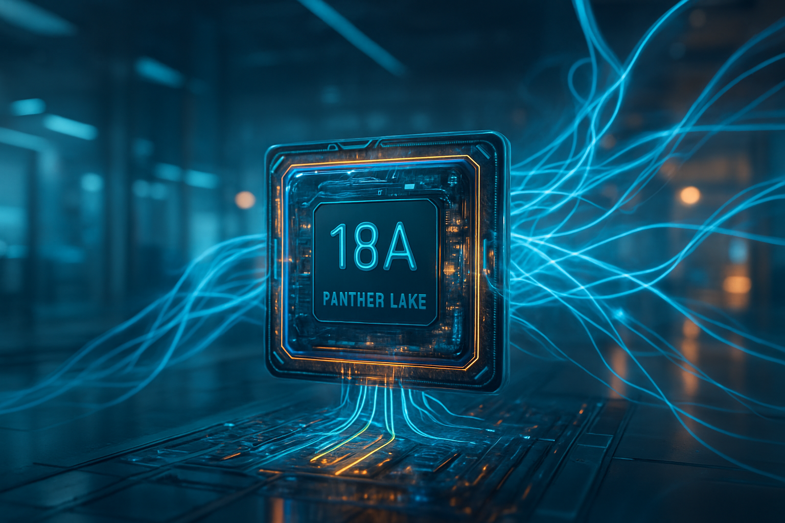
  • Intel’s 1.8nm Era: Reclaiming the Silicon Crown as 18A Enters High-Volume Production

    Intel’s 1.8nm Era: Reclaiming the Silicon Crown as 18A Enters High-Volume Production

    SANTA CLARA, Calif. — In a historic milestone for the American semiconductor industry, Intel (NASDAQ: INTC) has officially announced that its 18A (1.8nm-class) process node has entered high-volume manufacturing (HVM). The announcement, made during the opening keynote of CES 2026, marks the successful completion of the company’s ambitious "five nodes in four years" roadmap. For the first time in nearly a decade, Intel appears to have parity—and by some technical measures, a clear lead—over its primary rival, Taiwan Semiconductor Manufacturing Company (NYSE: TSM), in the race to power the next generation of artificial intelligence.

    The immediate significance of 18A cannot be overstated. As AI models grow exponentially in complexity, the demand for chips that offer higher transistor density and significantly lower power consumption has reached a fever pitch. By reaching high-volume production with 18A, Intel is not just releasing a new processor; it is launching a fully-fledged foundry service capable of building the world’s most advanced AI accelerators for third-party clients. With anchor customers like Microsoft (NASDAQ: MSFT) and Amazon (NASDAQ: AMZN) already ramping up production on the node, the silicon landscape is undergoing its most radical shift since the invention of the integrated circuit.

    The Architecture of Leadership: RibbonFET and PowerVia

    The Intel 18A node represents a fundamental departure from the FinFET transistor architecture that has dominated the industry for over a decade. At the heart of 18A are two "world-first" technologies: RibbonFET and PowerVia. RibbonFET is Intel’s implementation of a Gate-All-Around (GAA) transistor, where the gate wraps entirely around the conducting channel. This provides superior electrostatic control, drastically reducing current leakage and allowing for higher drive currents at lower voltages. While TSMC (NYSE: TSM) has also moved to GAA with its N2 node, Intel’s 18A is distinguished by its integration of PowerVia—the industry’s first backside power delivery system.

    PowerVia solves one of the most persistent bottlenecks in chip design: "voltage droop" and signal interference. In traditional chips, power and signal lines are intertwined on the front side of the wafer, competing for space. PowerVia moves the entire power delivery network to the back of the wafer, leaving the front exclusively for data signals. This separation allows for a 15% to 25% improvement in performance-per-watt and enables chips to run at higher clock speeds without overheating. Initial data from early 18A production runs indicates that Intel has achieved a transistor density of approximately 238 million transistors per square millimeter (MTr/mm²), providing a potent combination of raw speed and energy efficiency that is specifically tuned for AI workloads.

    Industry experts have reacted with cautious optimism, noting that while TSMC’s N2 node still holds a slight lead in pure area density, Intel’s lead in backside power delivery gives it a strategic "performance-per-watt" advantage that is critical for massive data centers. "Intel has effectively leapfrogged the industry in power delivery architecture," noted one senior analyst at the event. "While the competition is still figuring out how to untangle their power lines, Intel is already shipping at scale."

    A New Titan in the Foundry Market

    The arrival of 18A transforms Intel Foundry from a theoretical competitor into a genuine threat to the TSMC-Samsung duopoly. By securing Microsoft (NASDAQ: MSFT) as a primary customer for its custom "Maia 2" AI accelerators, Intel has proven that its foundry model can attract the world’s largest "hyperscalers." Amazon (NASDAQ: AMZN) has similarly committed to 18A for its custom AI fabric and Graviton-series processors, seeking to reduce its reliance on external suppliers and optimize its internal cloud infrastructure for the generative AI era.

    This development creates a complex competitive dynamic for AI leaders like NVIDIA (NASDAQ: NVDA). While NVIDIA remains heavily reliant on TSMC for its current H-series and B-series GPUs, the company reportedly made a strategic $5 billion investment in Intel’s advanced packaging capabilities in 2025. With 18A now in high-volume production, the industry is watching closely to see if NVIDIA will shift a portion of its next-generation "Rubin" or "Post-Rubin" architecture to Intel’s fabs to diversify its supply chain and hedge against geopolitical risks in the Taiwan Strait.

    For startups and smaller AI labs, the emergence of a high-performance alternative in the United States could lower the barrier to entry for custom silicon. Intel’s "Secure Enclave" partnership with the U.S. Department of Defense further solidifies 18A as the premier node for sovereign AI applications, ensuring that the most sensitive government and defense chips are manufactured on American soil using the most advanced process technology available.

    The Geopolitics of Silicon and the AI Landscape

    The success of 18A is a pivotal moment for the broader AI landscape, which has been plagued by hardware shortages and energy constraints. As AI training clusters grow to consume hundreds of megawatts, the efficiency gains provided by PowerVia and RibbonFET are no longer just "nice-to-have" features—they are economic imperatives. Intel’s ability to deliver more "compute-per-watt" directly impacts the total cost of ownership for AI companies, potentially slowing the rise of energy costs associated with LLM (Large Language Model) development.

    Furthermore, 18A represents the first major fruit of the CHIPS and Science Act, which funneled billions into domestic semiconductor manufacturing. The fact that this node is being produced at scale in Fab 52 in Chandler, Arizona, signals a shift in the global center of gravity for high-end manufacturing. It alleviates concerns about the "single point of failure" in the global AI supply chain, providing a robust, domestic alternative to East Asian foundries.

    However, the transition is not without concerns. The complexity of 18A manufacturing is immense, and maintaining high yields at 1.8nm is a feat of engineering that requires constant vigilance. While current yields are reported in the 65%–75% range, any dip in production efficiency could lead to supply shortages or increased costs for customers. Comparisons to previous milestones, such as the transition to EUV (Extreme Ultraviolet) lithography, suggest that the first year of a new node is always a period of intense "learning by doing."

    The Road to 14A and High-NA EUV

    Looking ahead, Intel is already preparing the successor to 18A: the 14A (1.4nm) node. While 18A relies on standard 0.33 NA EUV lithography with multi-patterning, 14A will be the first node to fully utilize ASML (NASDAQ: ASML) High-NA (Numerical Aperture) EUV machines. Intel was the first in the industry to receive these "Twinscan EXE:5200" tools, and the company is currently using them for risk production and R&D to refine the 1.4nm process.

    The near-term roadmap includes the launch of Intel’s "Panther Lake" mobile processors and "Clearwater Forest" server chips, both built on 18A. These products will serve as the "canary in the coal mine" for the node’s real-world performance. If Clearwater Forest, with its massive 288-core count, can deliver on its promised efficiency gains, it will likely trigger a wave of data center upgrades across the globe. Experts predict that by 2027, the industry will transition into the "Angstrom Era" entirely, where 18A and 14A become the baseline for all high-end AI and edge computing devices.

    A Resurgent Intel in the AI History Books

    The entry of Intel 18A into high-volume production is more than just a technical achievement; it is a corporate resurrection. After years of delays and lost leadership, Intel has successfully executed a "Manhattan Project" style turnaround. By betting early on backside power delivery and securing the world’s first High-NA EUV tools, Intel has positioned itself as the primary architect of the hardware that will define the late 2020s.

    In the history of AI, the 18A node will likely be remembered as the point where hardware efficiency finally began to catch up with software ambition. The long-term impact will be felt in everything from the battery life of AI-integrated smartphones to the carbon footprint of massive neural network training runs. For the coming months, the industry will be watching yield reports and customer testimonials with intense scrutiny. If Intel can sustain this momentum, the "silicon crown" may stay in Santa Clara for a long time to come.


    This content is intended for informational purposes only and represents analysis of current AI developments.

    TokenRing AI delivers enterprise-grade solutions for multi-agent AI workflow orchestration, AI-powered development tools, and seamless remote collaboration platforms.
    For more information, visit https://www.tokenring.ai/.