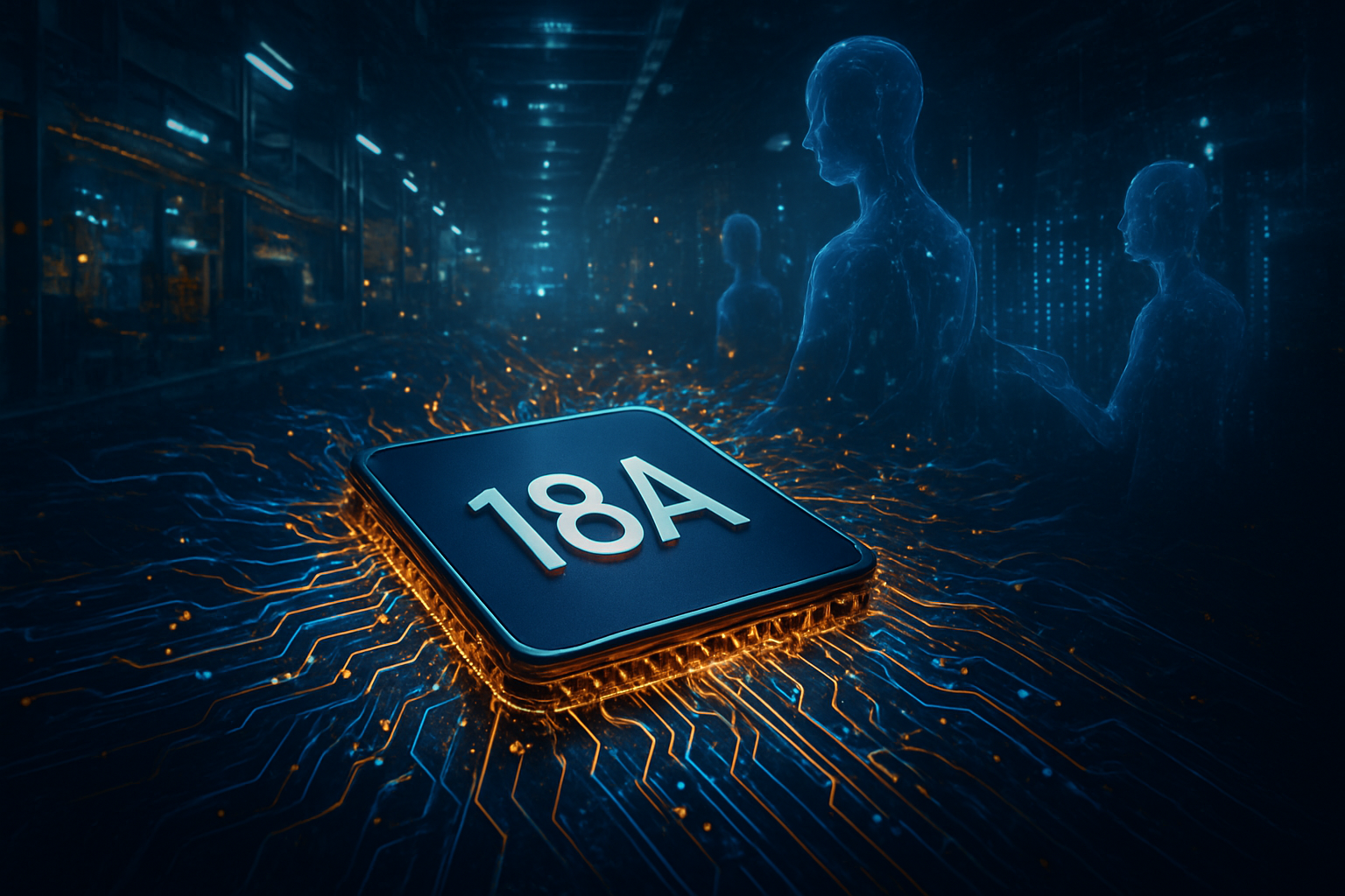
Tag: Intel

  • The Great Decoupling: NVIDIA’s Data Center Revenue Now Six Times Larger Than Intel and AMD Combined

    The Great Decoupling: NVIDIA’s Data Center Revenue Now Six Times Larger Than Intel and AMD Combined

    As of January 8, 2026, the global semiconductor landscape has reached a definitive tipping point, marking the end of the "CPU-first" era that defined computing for nearly half a century. Recent financial disclosures for the final quarters of 2025 have revealed a staggering reality: NVIDIA (NASDAQ: NVDA) now generates more revenue from its data center segment alone than the combined data center and CPU revenues of its two largest historical rivals, Intel (NASDAQ: INTC) and AMD (NASDAQ: AMD). This financial chasm—with NVIDIA’s $51.2 billion in quarterly data center revenue dwarfing the $8.4 billion combined total of its competitors—signals a permanent shift in the industry’s center of gravity toward accelerated computing.

    The disparity is even more pronounced when isolating for general-purpose CPUs. Analysts estimate that NVIDIA's data center revenue is now approximately eight times the combined server CPU revenue of Intel and AMD. This "Great Decoupling" highlights a fundamental change in how the world’s most powerful computers are built. No longer are GPUs merely "accelerators" added to a CPU-based system; in the modern "AI Factory," the GPU is the primary compute engine, and the CPU has been relegated to a supporting role, managing housekeeping tasks while NVIDIA’s Blackwell architecture performs the heavy lifting of modern intelligence.

    The Blackwell Era and the Rise of the Integrated Platform

    The primary catalyst for this financial explosion has been the unprecedented ramp-up of NVIDIA’s Blackwell architecture. Throughout 2025, the B200 and GB200 chips became the most sought-after commodities in the tech world. Unlike previous generations where chips were sold individually, NVIDIA’s dominance in 2025 was driven by the sale of entire integrated systems, such as the NVL72 rack. These systems combine 72 Blackwell GPUs with NVIDIA’s own Grace CPUs and high-speed BlueField-3 DPUs, creating a unified "superchip" environment that competitors have struggled to replicate.

    Technically, the shift is driven by the transition from "Training" to "Reasoning." While 2023 and 2024 were defined by training Large Language Models (LLMs), 2025 saw the rise of "Reasoning AI"—models that perform complex multi-step thinking during inference. These models require massive amounts of memory bandwidth and inter-chip communication, areas where NVIDIA’s proprietary NVLink interconnect technology provides a significant moat. While AMD (NASDAQ: AMD) has made strides with its MI325X and MI350 series, and Intel has attempted to gain ground with its Gaudi 3 accelerators, NVIDIA’s ability to provide a full-stack solution—including the CUDA software layer and Spectrum-X networking—has made it the default choice for hyperscalers.

    Initial reactions from the research community suggest that the industry is no longer just buying "chips," but "time-to-market." The integration of hardware and software allows AI labs to deploy clusters of 100,000+ GPUs and begin training or serving models almost immediately. This "plug-and-play" capability at a massive scale has effectively locked in the world’s largest spenders, including Microsoft (NASDAQ: MSFT), Meta (NASDAQ: META), and Alphabet (NASDAQ: GOOGL), who are currently locked in a "Prisoner's Dilemma" where they must continue to spend record amounts on NVIDIA hardware to avoid falling behind in the AI arms race.

    Competitive Implications and the Shrinking CPU Pie

    The strategic implications for the rest of the semiconductor industry are profound. For Intel (NASDAQ: INTC), the rise of NVIDIA has forced a painful pivot toward its Foundry business. While Intel’s "Panther Lake" CPUs remain competitive in the dwindling market for general-purpose server chips, the company’s Data Center and AI (DCAI) segment has stagnated, hovering around $4 billion per quarter. Intel is now betting its future on becoming the primary manufacturer for other chip designers, including potentially its own rivals, as it struggles to regain its footing in the high-margin AI accelerator market.

    AMD (NASDAQ: AMD) has fared better in terms of market share, successfully capturing nearly 30% of the server CPU market from Intel by late 2025. However, this victory is increasingly viewed as a "king of the hill" battle on a shrinking mountain. As data center budgets shift toward GPUs, the total addressable market for CPUs is not growing at the same rate as the overall AI infrastructure spend. AMD’s Instinct GPU line has seen healthy growth, reaching several billion in revenue, but it still lacks the software ecosystem and networking integration that allows NVIDIA to command 75%+ gross margins.

    Startups and smaller AI labs are also feeling the squeeze. The high cost of NVIDIA’s top-tier Blackwell systems has created a two-tier AI landscape: "compute-rich" giants who can afford the latest $3 million racks, and "compute-poor" entities that must rely on older Hopper (H100) hardware or cloud rentals. This has led to a surge in demand for AI orchestration platforms that can maximize the efficiency of existing hardware, as companies look for ways to extract more performance from their multi-billion dollar investments.

    The Broader AI Landscape: From Components to Sovereign Clouds

    This shift fits into a broader trend of "Sovereign AI," where nations are now building their own domestic data centers to ensure data privacy and technological independence. In late 2025, countries like Saudi Arabia, the UAE, and Japan emerged as major NVIDIA customers, purchasing entire AI factories to fuel their national AI initiatives. This has diversified NVIDIA’s revenue stream beyond the "Big Four" US hyperscalers, further insulating the company from any potential cooling in Silicon Valley venture capital.

    The wider significance of NVIDIA’s $50 billion quarters cannot be overstated. It represents the most rapid reallocation of capital in industrial history. Comparisons are often made to the build-out of the internet in the late 1990s, but with a key difference: the AI build-out is generating immediate, tangible revenue for the infrastructure provider. While the "dot-com" era saw massive spending on fiber optics that took a decade to utilize, NVIDIA’s Blackwell chips are often sold out 12 months in advance, with demand for "Inference-as-a-Service" growing as fast as the hardware can be manufactured.

    However, this dominance has also raised concerns. Regulators in the US and EU have increased their scrutiny of NVIDIA’s "moat," specifically focusing on whether the bundling of CUDA software with hardware constitutes anti-competitive behavior. Furthermore, the sheer energy requirements of these GPU-dense data centers have led to a secondary crisis in power generation, with NVIDIA now frequently partnering with energy companies to secure the gigawatts of electricity needed to run its latest clusters.

    Future Horizons: Vera Rubin and the $500 Billion Visibility

    Looking ahead to the remainder of 2026 and 2027, NVIDIA has already signaled its next move with the announcement of the "Vera Rubin" platform. Named after the astronomer who discovered evidence of dark matter, the Rubin architecture is expected to focus on "Unified Compute," further blurring the lines between networking, memory, and processing. Experts predict that NVIDIA will continue its transition toward becoming a "Data Center-as-a-Service" company, potentially offering its own cloud capacity to compete directly with the very hyperscalers that are currently its largest customers.

    Near-term developments will likely focus on "Edge AI" and "Physical AI" (robotics). As the cost of inference drops due to Blackwell’s efficiency, we expect to see more complex AI models running locally on devices and within industrial robots. The challenge will be the "power wall"—the physical limit of how much heat can be dissipated and how much electricity can be delivered to a single rack. Addressing this will require breakthroughs in liquid cooling and power delivery, areas where NVIDIA is already investing heavily through its ecosystem of partners.

    A Permanent Shift in the Computing Hierarchy

    The data from early 2026 confirms that NVIDIA is no longer just a chip company; it is the architect of the AI era. By capturing more revenue than the combined forces of the traditional CPU industry, NVIDIA has proved that the future of computing is accelerated, parallel, and deeply integrated. The "CPU-centric" world of the last 40 years has been replaced by an "AI-centric" world where the GPU is the heart of the machine.

    Key takeaways for the coming months include the continued ramp-up of Blackwell, the first real-world benchmarks of the Vera Rubin architecture, and the potential for a "second wave" of AI investment from enterprise customers who are finally moving their AI pilots into full-scale production. While the competition from AMD and the manufacturing pivot of Intel will continue, the "center of gravity" has moved. For the foreseeable future, the world’s digital infrastructure will be built on NVIDIA’s terms.


    This content is intended for informational purposes only and represents analysis of current AI developments.

    TokenRing AI delivers enterprise-grade solutions for multi-agent AI workflow orchestration, AI-powered development tools, and seamless remote collaboration platforms.
    For more information, visit https://www.tokenring.ai/.

  • Intel Reclaims the Silicon Crown: Core Ultra Series 3 ‘Panther Lake’ Debuts at CES 2026 as First US-Made 18A AI PC Chip

    Intel Reclaims the Silicon Crown: Core Ultra Series 3 ‘Panther Lake’ Debuts at CES 2026 as First US-Made 18A AI PC Chip

    In a landmark moment for the global semiconductor industry, Intel (NASDAQ:INTC) officially launched its Core Ultra Series 3 processors, codenamed "Panther Lake," at CES 2026. Unveiled by senior leadership at the Las Vegas tech showcase, Panther Lake represents more than just a seasonal hardware refresh; it is the first consumer-grade silicon built on the Intel 18A process node, manufactured entirely within the United States. This launch marks the culmination of Intel’s ambitious "five nodes in four years" strategy, signaling a definitive return to the forefront of manufacturing technology.

    The immediate significance of Panther Lake lies in its role as the engine for the next generation of "Agentic AI PCs." With a dedicated Neural Processing Unit (NPU) delivering 50 TOPS (Trillions of Operations Per Second) and a total platform throughput of 180 TOPS, Intel is positioning these chips to handle complex, autonomous AI agents locally on the device. By combining cutting-edge domestic manufacturing with unprecedented AI performance, Intel is not only challenging its rivals but also reinforcing the strategic importance of a resilient, US-based semiconductor supply chain.

    The 18A Breakthrough: RibbonFET and PowerVia Take Center Stage

    Technically, Panther Lake is a marvel of modern engineering, representing the first large-scale implementation of two foundational innovations: RibbonFET and PowerVia. RibbonFET is Intel’s implementation of a gate-all-around (GAA) transistor architecture, which replaces the long-standing FinFET design. This allows for better electrostatic control and higher drive current at lower voltages, resulting in a 15% improvement in performance-per-watt over previous generations. Complementing this is PowerVia, the industry's first backside power delivery system. By moving power routing to the back of the wafer, Intel has eliminated traditional bottlenecks in transistor density and reduced voltage droop, allowing the chip to run more efficiently under heavy AI workloads.

    At the heart of Panther Lake’s AI capabilities is the NPU 5 architecture. While the previous generation "Lunar Lake" met the 40 TOPS threshold for Microsoft (NASDAQ:MSFT) Copilot+ certification, Panther Lake pushes the dedicated NPU to 50 TOPS. When the NPU works in tandem with the new Xe3 "Celestial" graphics architecture and the high-performance Cougar Cove CPU cores, the total platform performance reaches a staggering 180 TOPS. This leap is specifically designed to enable "Small Language Models" (SLMs) and vision-action models to run with near-zero latency, allowing for real-time privacy-focused AI assistants that don't rely on the cloud.

    The integrated graphics also see a massive overhaul. The Xe3 Celestial architecture, marketed under the Arc B-Series umbrella, features up to 12 Xe3 cores. Intel claims this provides a 77% increase in gaming performance compared to the Core Ultra 9 285H. Beyond gaming, these GPU cores are equipped with XMX engines that provide the bulk of the platform’s 180 TOPS, making the chip a powerhouse for local generative AI tasks like image creation and video upscaling.

    Initial reactions from the industry have been overwhelmingly positive. Analysts from the AI research community have noted that Panther Lake’s focus on "total platform TOPS" rather than just NPU throughput reflects a more mature understanding of how AI software actually utilizes hardware. By spreading the load across the CPU, GPU, and NPU, Intel is providing developers with a more flexible playground for building the next generation of software.

    Reshaping the Competitive Landscape: Intel vs. The World

    The launch of Panther Lake creates immediate pressure on Intel’s primary competitors: AMD (NASDAQ:AMD), Qualcomm (NASDAQ:QCOM), and Apple (NASDAQ:AAPL). While Qualcomm’s Snapdragon X2 Elite currently holds the lead in raw NPU throughput with 80 TOPS, Intel’s "total platform" approach and superior integrated graphics offer a more balanced package for power users and gamers. AMD’s Ryzen AI 400 series, also debuting at CES 2026, competes closely with a 60 TOPS NPU, but Intel’s transition to the 18A node gives it a density and power efficiency advantage that AMD, still largely reliant on TSMC (NYSE:TSM) for manufacturing, may struggle to match in the short term.

    For tech giants like Dell (NYSE:DELL), HP (NYSE:HPQ), and ASUS, Panther Lake provides the high-performance silicon needed to justify a new upgrade cycle for enterprise and consumer laptops. These manufacturers have already announced over 200 designs based on the new architecture, many of which focus on "AI-first" features like automated workflow orchestration and real-time multi-modal translation. The ability to run these tasks locally reduces cloud costs for enterprises, making Intel-powered AI PCs an attractive proposition for IT departments.

    Furthermore, the success of the 18A node is a massive win for the Intel Foundry business. With Panther Lake proving that 18A is ready for high-volume production, external customers like Amazon (NASDAQ:AMZN) and the U.S. Department of Defense are likely to accelerate their own 18A-based projects. This positions Intel not just as a chip designer, but as a critical manufacturing partner for the entire tech industry, potentially disrupting the long-standing dominance of TSMC in the leading-edge foundry market.

    A Geopolitical Milestone: The Return of US Silicon Leadership

    Beyond the spec sheets, Panther Lake carries immense weight in the broader context of global technology and geopolitics. For the first time in over a decade, the world’s most advanced semiconductor process node is being manufactured in the United States, specifically at Intel’s Fab 52 in Arizona. This is a direct victory for the CHIPS and Science Act, which sought to revitalize domestic manufacturing and reduce reliance on overseas supply chains.

    The strategic importance of this cannot be overstated. As AI becomes a central pillar of national security and economic competitiveness, having a domestic source of leading-edge AI silicon is a critical advantage. The U.S. government’s involvement through the RAMP-C project ensures that the same 18A technology powering consumer laptops will also underpin the next generation of secure defense systems.

    However, this shift also brings concerns regarding the sustainability of such massive energy requirements. The production of 18A chips involves High-NA EUV lithography, a process that is incredibly energy-intensive. As Intel scales this production, the industry will be watching closely to see how the company balances its manufacturing ambitions with its environmental and social governance (ESG) goals. Nevertheless, compared to previous milestones like the introduction of the first 64-bit processors or the shift to multi-core architectures, the move to 18A and integrated AI represents a more fundamental shift in how computing power is generated and deployed.

    The Horizon: From AI PCs to Autonomous Systems

    Looking ahead, Panther Lake is just the beginning of Intel’s 18A journey. The company has already teased its next-generation "Clearwater Forest" Xeon processors for data centers and the future "14A" node, which is expected to push boundaries even further by 2027. In the near term, we can expect to see a surge in "Agentic" software—applications that don't just respond to prompts but proactively manage tasks for the user. With 50+ TOPS of NPU power, these agents will be able to "see" what is on a user's screen and "act" across different applications securely and privately.

    The challenges remaining are largely on the software side. While the hardware is now capable of 180 TOPS, the ecosystem of developers must catch up to utilize this power effectively. We expect to see Microsoft release a major Windows "AI Edition" update later this year that specifically targets the capabilities of Panther Lake and its contemporaries, potentially moving the operating system's core functions into the AI domain.

    Closing the Chapter on the "Foundry Gap"

    In summary, the launch of the Core Ultra Series 3 "Panther Lake" at CES 2026 is a defining moment for Intel and the American tech industry. By successfully delivering a 1.8nm-class processor with a 50 TOPS NPU and high-end integrated graphics, Intel has proved that it can still innovate at the bleeding edge of physics. The 18A node is no longer a roadmap promise; it is a shipping reality that re-establishes Intel as a formidable leader in both chip design and manufacturing.

    As we move into the first quarter of 2026, the industry will be watching the retail performance of these chips and the stability of the 18A yields. If Intel can maintain this momentum, the "Foundry Gap" that has defined the last five years of the semiconductor industry may finally be closed. For now, the AI PC has officially entered its most powerful era yet, and for the first time in a long time, the heart of that innovation is beating in the American Southwest.


    This content is intended for informational purposes only and represents analysis of current AI developments.

    TokenRing AI delivers enterprise-grade solutions for multi-agent AI workflow orchestration, AI-powered development tools, and seamless remote collaboration platforms.
    For more information, visit https://www.tokenring.ai/.

  • The Silicon Super-Cycle: US Implements ‘Managed Bifurcation’ as Semiconductor Market nears $1 Trillion

    The Silicon Super-Cycle: US Implements ‘Managed Bifurcation’ as Semiconductor Market nears $1 Trillion

    As of January 8, 2026, the global semiconductor industry has entered a transformative era defined by what economists call the "Silicon Super-Cycle." With total annual revenue rapidly approaching the $1 trillion milestone, the geopolitical landscape has shifted from a chaotic trade war to a sophisticated state of "managed bifurcation." The United States government, moving beyond passive regulation, has emerged as an active market participant, implementing a groundbreaking revenue-sharing model for AI exports while simultaneously executing strategic interventions to protect domestic interests.

    This new paradigm was punctuated last week by the blocking of a sensitive acquisition and the revelation of a massive federal stake in the nation’s leading chipmaker. These moves signal a definitive end to the era of globalized, borderless silicon and the beginning of a world where advanced compute capacity is treated with the same strategic gravity as nuclear enrichment or oil reserves.

    The Revenue-Sharing Pivot and the 2nm Frontier

    The technical and policy centerpiece of early 2026 is the US Department of Commerce’s "reversal-for-revenue" strategy. In a surprising late-2025 policy shift, the US administration granted NVIDIA Corporation (NASDAQ: NVDA) permission to resume shipments of its high-performance H200 AI chips to select customers in China. However, this comes with a historic caveat: a mandatory 25% "geopolitical risk tax" on every unit sold, paid directly to the US Treasury. This model attempts to balance the commercial needs of American tech giants with the national security goal of funding domestic infrastructure through the profits of competitors.

    Technologically, the industry has reached the 2-nanometer (2nm) milestone. Taiwan Semiconductor Manufacturing Company (NYSE: TSM) reported this week that its N2 process has achieved commercial yields of nearly 70%, significantly ahead of internal projections. This leap allows for a 15% increase in speed or a 30% reduction in power consumption compared to the previous 3nm generation. This advancement is critical as the "Intelligence Economy" demands more efficient hardware to sustain the massive energy requirements of generative AI models that have now moved from text and image generation into real-time, high-fidelity world simulation.

    Initial reactions from the AI research community have been mixed. While the availability of H200-class hardware in China provides a temporary relief valve for global supply chains, industry experts note that the 25% tax effectively creates a "compute divide." Researchers in the West are already eyeing the next generation of Blackwell-Ultra and Rubin architectures, while Chinese firms are being forced to choose between heavily taxed US silicon or domestic alternatives like Huawei’s Ascend series, which Beijing is now mandating for state-level projects.

    Corporate Giants and the Rise of 'Sovereign AI'

    The corporate impact of these shifts is most visible in the partial "nationalization" of Intel Corporation (NASDAQ: INTC). Following a period of financial volatility in late 2025, the US government intervened with an $8.9 billion stock purchase, funded by the Secure Enclave program. This move ensures that the Department of Defense has a guaranteed, domestic source for leading-edge military and intelligence chips. Intel is now effectively a public-private partnership, focused on its Arizona and Oregon "Secure Enclaves" to maintain a "frontier compute" lead over global rivals.

    NVIDIA, meanwhile, is navigating a complex dual-market strategy. While facing a soft boycott in China—where Beijing has directed local firms to halt H200 orders in favor of domestic chips—the company has found a massive new growth engine in the Middle East. In late December 2025, the US greenlit a $1 billion shipment of 35,000 advanced chips to Saudi Arabia’s HUMAIN project and the UAE’s G42. This deal was contingent on the total removal of Chinese hardware from those nations' data centers, illustrating how the US is using its "silicon hegemony" to forge new diplomatic and technological alliances.

    Other major players like Advanced Micro Devices, Inc. (NASDAQ: AMD) and ASML Holding N.V. (NASDAQ: ASML) are adjusting to this highly regulated environment. AMD has seen increased demand for its MI350 series in markets where NVIDIA’s tax-heavy H200s are less competitive, while ASML continues to face tightening restrictions on the export of its High-NA EUV lithography machines, further cementing the "technological moat" around the US and its immediate allies.

    Geopolitical Friction and the 'Third Path'

    The wider significance of these developments lies in the aggressive stance the US is taking against even minor "on-ramps" for foreign influence. On January 2, 2026, a Presidential Executive Order blocked the $3 million acquisition of assets from Emcore Corporation (NASDAQ: EMKR) by HieFo Corp, a firm identified as having ties to Chinese nationals. While the deal was small in dollar terms, the focus was on Emcore’s expertise in indium phosphide (InP) chips—a technology vital for military lasers and advanced sensors. This underscores a policy of "zero-leakage" for dual-use technologies.

    In Europe, a "Third Path" is emerging. All 27 EU member states recently signed a declaration calling for "EU Chips Act 2.0," with a formal review scheduled for the first quarter of 2026. The goal is to secure €20 billion in additional funding to help Europe reach a 20% global market share by 2030. The EU is positioning itself as the global leader in specialized "specialty" chips for the automotive and industrial sectors, attempting to remain a neutral ground while the US and China continue their high-stakes compute race.

    This landscape is a stark departure from the early 2020s. We are no longer seeing a "chip shortage" driven by supply chain hiccups, but a "compute containment" strategy. The US is leveraging its 8:1 advantage in frontier compute capacity to dictate the terms of the global AI rollout, while China counters by leveraging its dominance in the critical mineral supply chains—gallium, germanium, and rare earths—necessary to build the next generation of hardware.

    The Road to 2030: Challenges and Predictions

    Looking ahead, the next 12 to 24 months will likely see the formalization of "CHIPS 2.0" in the United States. Rather than just building factories, the focus is shifting toward fraud risk management and the oversight of the original $50 billion fund. Experts predict that by 2027, the US will attempt to create a "Silicon NATO"—a formal alliance of nations that share compute resources and research while maintaining a unified export front against non-aligned states.

    A major challenge remains the "Malaysia Shift." Companies like Nexperia, currently under pressure due to Chinese ownership, are rapidly moving production to Southeast Asia to avoid "penetrating sanctions." This migration is creating a new semiconductor hub in Malaysia and Vietnam, which could eventually challenge the established order if they can move up the value chain from assembly and testing to actual wafer fabrication.

    Predicting the next move, analysts suggest that the "Intelligence Economy" will drive the semiconductor market toward $1.5 trillion by 2030. The primary hurdle will not be the physics of the chips themselves, but the geopolitical friction of their distribution. As AI models become more integrated into national infrastructure, the "sovereignty" of the silicon they run on will become the most important metric for any nation's security.

    Summary of the New Silicon Order

    The events of early 2026 mark a definitive turning point in the history of technology. The transition from free-market competition to "managed bifurcation" reflects the reality that semiconductors are now the foundational resource of the 21st century. The US government’s active role—from taking stakes in Intel to taxing NVIDIA’s exports—shows that the "invisible hand" of the market has been replaced by the strategic hand of the state.

    Key takeaways for the coming weeks include the EU’s formal decision on Chips Act 2.0 funding and the potential for a Chinese counter-response regarding critical mineral exports. As we monitor these developments, the central question remains: can the world sustain a $1 trillion industry that is increasingly divided by digital iron curtains, or will the cost of bifurcation eventually stifle the very AI revolution it seeks to control?


    This content is intended for informational purposes only and represents analysis of current AI developments.

    TokenRing AI delivers enterprise-grade solutions for multi-agent AI workflow orchestration, AI-powered development tools, and seamless remote collaboration platforms.
    For more information, visit https://www.tokenring.ai/.

  • The Backside Revolution: How PowerVia and A16 Are Rewiring the Future of AI Silicon

    The Backside Revolution: How PowerVia and A16 Are Rewiring the Future of AI Silicon

    As of January 8, 2026, the semiconductor industry has reached a historic inflection point that promises to redefine the limits of artificial intelligence hardware. For decades, chip designers have struggled with a fundamental physical bottleneck: the "front-side" delivery of power, where power lines and signal wires compete for the same cramped real estate on top of transistors. Today, that bottleneck is being shattered as Backside Power Delivery (BSPD) officially enters high-volume manufacturing, led by Intel Corporation (NASDAQ: INTC) and its groundbreaking 18A process.

    The shift to backside power—marketing-branded as "PowerVia" by Intel and "Super PowerRail" by Taiwan Semiconductor Manufacturing Company (NYSE: TSM)—is more than a mere manufacturing tweak; it is a fundamental architectural reorganization of the microchip. By moving the power delivery network to the underside of the silicon wafer, manufacturers are unlocking unprecedented levels of power efficiency and transistor density. This development arrives at a critical moment for the AI industry, where the ravenous energy demands of next-generation Large Language Models (LLMs) have threatened to outpace traditional hardware improvements.

    The Technical Leap: Decoupling Power from Logic

    Intel's 18A process, which reached high-volume manufacturing at Fab 52 in Chandler, Arizona, earlier this month, represents the first commercial deployment of Backside Power Delivery at scale. The core innovation, PowerVia, works by separating the intricate web of signal wires from the power delivery lines. In traditional chips, power must "tunnel" through up to 15 layers of metal interconnects to reach the transistors, leading to significant "voltage droop" and electrical interference. PowerVia eliminates this by routing power through the back of the wafer using Nano-Through Silicon Vias (nTSVs), providing a direct, low-resistance path to the transistors.

    The technical specifications of Intel 18A are formidable. By implementing PowerVia alongside RibbonFET (Gate-All-Around) transistors, Intel has achieved a 30% reduction in voltage droop and a 6% boost in clock frequency at identical power levels compared to previous generations. More importantly for AI chip designers, the technology allows for 90% standard cell utilization, drastically reducing the "wiring congestion" that often forces engineers to leave valuable silicon area empty. This leap in logic density—exceeding 30% over the Intel 3 node—means more AI processing cores can be packed into the same physical footprint.

    Initial reactions from the semiconductor research community have been overwhelmingly positive. Dr. Arati Prabhakar, Director of the White House Office of Science and Technology Policy, noted during a recent briefing that "the successful ramp of 18A is a validation of the 'five nodes in four years' strategy and a pivotal moment for domestic advanced manufacturing." Industry experts at SemiAnalysis have highlighted that Intel’s decision to decouple PowerVia from its first Gate-All-Around node (Intel 20A) allowed the company to de-risk the technology, giving them a roughly 18-month lead over TSMC in mastering the complexities of backside thinning and via alignment.

    The Competitive Landscape: Intel’s First-Mover Advantage vs. TSMC’s A16 Response

    The arrival of 18A has sent shockwaves through the foundry market, placing Intel Corporation (NASDAQ: INTC) in a rare position of technical leadership over TSMC. Intel has already secured major 18A commitments from Microsoft (NASDAQ: MSFT) and Amazon (NASDAQ: AMZN) for their custom AI accelerators, Maieutics and Trainium 3, respectively. By being the first to offer a mature BSPD solution, Intel Foundry is positioning itself as the premier destination for "AI-first" silicon, where thermal management and power delivery are the primary design constraints.

    However, TSMC is not standing still. The world’s largest foundry is preparing its response in the form of the A16 node, scheduled for high-volume manufacturing in the second half of 2026. TSMC’s implementation, known as Super PowerRail, is technically more ambitious than Intel’s PowerVia. While Intel uses nTSVs to connect to the metal layers, TSMC’s Super PowerRail connects the power network directly to the source and drain of the transistors. This "direct-contact" approach is significantly harder to manufacture but is expected to offer an 8-10% speed increase and a 15-20% power reduction, potentially leapfrogging Intel’s performance metrics by late 2026.

    The strategic battle lines are clearly drawn. Nvidia (NASDAQ: NVDA), the undisputed leader in AI hardware, has reportedly signed on as the anchor customer for TSMC’s A16 node to power its 2027 "Feynman" GPU architecture. Meanwhile, Apple (NASDAQ: AAPL) is rumored to be taking a more cautious approach, potentially skipping A16 for its mobile chips to focus on the N2P node, suggesting that backside power is currently viewed as a premium feature specifically optimized for high-performance computing and AI data centers rather than consumer mobile devices.

    Wider Significance: Solving the AI Power Crisis

    The transition to backside power delivery is a critical milestone in the broader AI landscape. As AI models grow in complexity, the "power wall"—the limit at which a chip can no longer be cooled or supplied with enough electricity—has become the primary obstacle to progress. BSPD effectively raises this wall. By reducing IR drop (voltage loss) and improving thermal dissipation, backside power allows AI accelerators to run at higher sustained workloads without throttling. This is essential for training the next generation of "Agentic AI" systems that require constant, high-intensity compute cycles.

    Furthermore, this development marks the end of the "FinFET era" and the beginning of the "Angstrom era." The move to 18A and A16 represents a transition where traditional scaling (making things smaller) is being replaced by architectural scaling (rearranging how things are built). This shift mirrors previous milestones like the introduction of High-K Metal Gate (HKMG) or EUV lithography, both of which were necessary to keep Moore’s Law alive. In 2026, the "Backside Revolution" is the new prerequisite for remaining competitive in the global AI arms race.

    There are, however, concerns regarding the complexity and cost of these new processes. Backside power requires extremely precise wafer thinning—grinding the silicon down to a fraction of its original thickness—and complex bonding techniques. These steps increase the risk of wafer breakage and lower initial yields. While Intel has reported healthy 18A yields in the 55-65% range, the high cost of these chips may further consolidate power in the hands of "Big Tech" giants like Alphabet (NASDAQ: GOOGL) and Meta (NASDAQ: META), who are the only ones capable of affording the multi-billion dollar design and fabrication costs associated with 1.6nm and 1.8nm silicon.

    The Road Ahead: 1.4nm and the Future of AI Accelerators

    Looking toward the late 2020s, the trajectory of backside power is clear: it will become the standard for all high-performance logic. Intel is already planning its "14A" node for 2027, which will refine PowerVia with even denser interconnects. Simultaneously, Samsung Electronics (OTC: SSNLF) is preparing its SF2Z node for 2027, which will integrate its own version of BSPDN into its third-generation Gate-All-Around (MBCFET) architecture. Samsung’s entry will likely trigger a price war in the advanced foundry space, potentially making backside power more accessible to mid-sized AI startups and specialized ASIC designers.

    Beyond 2026, we expect to see "Backside Power 2.0," where manufacturers begin to move other components to the back of the wafer, such as decoupling capacitors or even certain types of memory (like RRAM). This could lead to "3D-stacked" AI chips where the logic is sandwiched between a backside power delivery layer and a front-side memory cache, creating a truly three-dimensional computing environment. The primary challenge remains the thermal density; as chips become more efficient at delivering power, they also become more concentrated heat sources, necessitating new liquid cooling or "on-chip" cooling technologies.

    Conclusion: A New Foundation for Artificial Intelligence

    The arrival of Intel’s 18A and the looming shadow of TSMC’s A16 mark the beginning of a new chapter in semiconductor history. Backside Power Delivery has transitioned from a laboratory curiosity to a commercial reality, providing the electrical foundation upon which the next decade of AI innovation will be built. By solving the "routing congestion" and "voltage droop" issues that have plagued chip design for years, PowerVia and Super PowerRail are enabling a new class of processors that are faster, cooler, and more efficient.

    The significance of this development cannot be overstated. In the history of AI, we will look back at 2026 as the year the industry "flipped the chip" to keep the promise of exponential growth alive. For investors and tech enthusiasts, the coming months will be defined by the ramp-up of Intel’s Panther Lake and Clearwater Forest processors, providing the first real-world benchmarks of what backside power can do. As TSMC prepares its A16 risk production in the first half of 2026, the battle for silicon supremacy has never been more intense—or more vital to the future of technology.


    This content is intended for informational purposes only and represents analysis of current AI developments.

    TokenRing AI delivers enterprise-grade solutions for multi-agent AI workflow orchestration, AI-powered development tools, and seamless remote collaboration platforms.
    For more information, visit https://www.tokenring.ai/.

  • Qualcomm Shatters AI PC Performance Barriers with Snapdragon X2 Elite Launch at CES 2026

    Qualcomm Shatters AI PC Performance Barriers with Snapdragon X2 Elite Launch at CES 2026

    The landscape of personal computing has undergone a seismic shift as Qualcomm (NASDAQ: QCOM) officially unveiled its next-generation Snapdragon X2 Elite and Snapdragon X2 Plus processors at CES 2026. This announcement marks a definitive turning point in the "AI PC" era, with Qualcomm delivering a staggering 80 TOPS (Trillions of Operations Per Second) of dedicated NPU performance—far exceeding the initial industry expectations of 50 TOPS. By standardizing this high-tier AI processing power across both its flagship and mid-range "Plus" silicon, Qualcomm is making a bold play to commoditize advanced on-device AI and dismantle the long-standing x86 hegemony in the Windows ecosystem.

    The immediate significance of the X2 series lies in its ability to power "Agentic AI"—background digital entities capable of executing complex, multi-step workflows autonomously. While previous generations focused on simple image generation or background blur, the Snapdragon X2 is designed to manage entire productivity chains, such as cross-referencing a week of emails to draft a project proposal while simultaneously monitoring local security threats. This launch effectively signals the end of the experimental phase for Windows-on-ARM, positioning Qualcomm not just as a mobile chipmaker entering the PC space, but as the primary architect of the modern AI workstation.

    Architectural Leap: The 80 TOPS Standard

    The technical architecture of the Snapdragon X2 series represents a complete overhaul of the initial Oryon design. Built on TSMC’s cutting-edge 3nm (N3P/N3X) process, the X2 Elite features the 3rd Generation Oryon CPU, which has transitioned to a sophisticated tiered core design. Unlike the first generation’s uniform core structure, the X2 Elite utilizes a "Big-Medium-Little" configuration, featuring high-frequency "Prime" cores that boost up to 5.0 GHz for bursty workloads, alongside dedicated efficiency cores that handle background tasks with minimal power draw. This architectural shift allows for a 43% reduction in power consumption compared to the previous Snapdragon X Elite while delivering a 25% increase in multi-threaded performance.

    At the heart of the silicon is the upgraded Hexagon NPU, which now delivers a uniform 80 TOPS across the entire product stack, including the 10-core and 6-core Snapdragon X2 Plus variants. This is a massive 78% generational leap in AI throughput. Furthermore, Qualcomm has integrated a new "Matrix Engine" directly into the CPU clusters. This engine is designed to handle "micro-AI" tasks—such as real-time language translation or UI predictive modeling—without needing to engage the main NPU, thereby reducing latency and further preserving battery life. Initial benchmarks from the AI research community show the X2 Plus 10-core scoring over 4,100 points in UL Procyon AI tests, nearly doubling the performance of current-gen competitors.

    Industry experts have reacted with particular interest to the X2 Elite's on-package memory integration. High-end "Extreme" SKUs now offer up to 128GB of LPDDR5x memory directly on the chip substrate, providing a massive 228 GB/s of bandwidth. This is a critical technical requirement for running Large Language Models (LLMs) with billions of parameters locally, ensuring that user data never has to leave the device for processing. By solving the memory bottleneck that plagued earlier AI PCs, Qualcomm has created a platform that can run sophisticated, private AI models with the same fluid responsiveness as cloud-based alternatives.

    Disrupting the x86 Hegemony

    Qualcomm’s aggressive push is creating a "silicon bloodbath" for traditional incumbents Intel (NASDAQ: INTC) and AMD (NASDAQ: AMD). For decades, the Windows market was defined by the x86 instruction set, but the X2 series' combination of 80 TOPS and 25-hour battery life is forcing a rapid re-evaluation. Intel’s latest "Panther Lake" chips, while highly capable, currently peak at 50 TOPS for their NPU, leaving a significant performance gap in specialized AI tasks. While Intel and AMD still hold the lead in legacy gaming and high-end workstation niches, Qualcomm is successfully capturing the high-volume "prosumer" and enterprise laptop segments that prioritize mobility and AI-driven productivity.

    The competitive landscape is further complicated by Qualcomm’s strategic focus on the enterprise market through its new "Snapdragon Guardian" technology. This hardware-level management suite directly challenges Intel’s vPro, offering IT departments the ability to remote-wipe, update, and secure laptops via the chip’s integrated 5G modem, even when the device is powered down. This move targets the lucrative corporate fleet market, where Intel has historically been unassailable. By offering better AI performance and superior remote management, Qualcomm is giving CIOs a compelling reason to switch architectures for the first time in twenty years.

    Major PC manufacturers like Dell (NYSE: DELL), HP (NYSE: HPQ), and Lenovo are the primary beneficiaries of this shift, as they can now offer a diverse range of "AI-first" laptops that compete directly with Apple's (NASDAQ: AAPL) MacBook Pro in terms of efficiency and power. Microsoft (NASDAQ: MSFT) also stands to gain immensely; the Snapdragon X2 provides the ideal hardware target for the next evolution of Windows 11 and the rumored "Windows 12," which are expected to lean even more heavily into integrated Copilot features that require the high TOPS count Qualcomm now provides as a standard.

    The End of the "App Gap" and the Rise of Local AI

    The broader significance of the Snapdragon X2 launch is the definitive resolution of the "App Gap" that once hindered ARM-based Windows devices. As of early 2026, Microsoft reports that users spend over 90% of their time in native ARM64 applications. With the Adobe Creative Cloud, Microsoft 365, and even specialized CAD software now running natively, the technical friction of switching from Intel to Qualcomm has virtually vanished. Furthermore, Qualcomm’s "Prism" emulation layer has matured to the point where 90% of the top-played Windows games run with minimal performance loss, effectively removing the last major barrier to consumer adoption.

    This development also marks a shift in how the industry defines "performance." We are moving away from raw CPU clock speeds and toward "AI Utility." The ability of the Snapdragon X2 to run 10-billion parameter models locally has profound implications for data privacy and security. By moving AI processing from the cloud to the edge, Qualcomm is addressing growing public concerns regarding data harvesting by major AI labs. This "Local-First" AI movement could fundamentally change the business models of SaaS companies, shifting the value from cloud subscriptions to high-performance local hardware.

    However, this transition is not without concerns. The rapid obsolescence of non-AI PCs could lead to a massive wave of electronic waste as corporations and consumers rush to upgrade to "NPU-capable" hardware. Additionally, the fragmentation of the Windows ecosystem between x86 and ARM, while narrowing, still presents challenges for niche software developers who must now maintain two separate codebases or rely on emulation. Despite these hurdles, the Snapdragon X2 represents the most significant milestone in PC architecture since the introduction of multi-core processing, signaling a future where the CPU is merely a support structure for the NPU.

    Future Horizons: From Laptops to the Edge

    Looking ahead, the next 12 to 24 months will likely see Qualcomm attempt to push the Snapdragon X2 architecture into even more form factors. Rumors are already circulating about a "Snapdragon X2 Ultra" designed for fanless desktop "mini-PCs" and high-end tablets that could rival the iPad Pro. In the long term, Qualcomm has stated its goal is to capture 50% of the Windows laptop market by 2029. To achieve this, the company will need to continue scaling its production and maintaining its lead in NPU performance as Intel and AMD inevitably close the gap with their 2027 and 2028 roadmaps.

    We can also expect to see the emergence of "Multi-Agent" OS environments. With 80 TOPS available locally, developers are likely to build software that utilizes multiple specialized AI agents working in parallel—one for security, one for creative assistance, and one for data management—all running simultaneously on the Hexagon NPU. The challenge for Qualcomm will be ensuring that the software ecosystem can actually utilize this massive overhead. Currently, the hardware is significantly ahead of the software; the "killer app" for an 80 TOPS NPU is still in development, but the headroom provided by the X2 series ensures that when it arrives, the hardware will be ready.

    Conclusion: A New Era of Silicon

    The launch of the Snapdragon X2 Elite and Plus chips is more than just a seasonal hardware refresh; it is an assertive declaration of Qualcomm's intent to lead the personal computing industry. By delivering 80 TOPS of NPU performance and a 3nm architecture that prioritizes efficiency without sacrificing power, Qualcomm has set a new benchmark that its competitors are now scrambling to meet. The standardization of high-end AI processing across its entire lineup ensures that the "AI PC" is no longer a luxury tier but the new baseline for all Windows users.

    As we move through 2026, the key metrics to watch will be Qualcomm's enterprise adoption rates and the continued evolution of Microsoft’s AI integration. If the Snapdragon X2 can maintain its momentum and continue to secure design wins from major OEMs, the decades-long "Wintel" era may finally be giving way to a more diverse, AI-centric silicon landscape. For now, Qualcomm holds the performance crown, and the rest of the industry is playing catch-up in a race where the finish line is constantly being moved by the rapid advancement of artificial intelligence.


    This content is intended for informational purposes only and represents analysis of current AI developments.

    TokenRing AI delivers enterprise-grade solutions for multi-agent AI workflow orchestration, AI-powered development tools, and seamless remote collaboration platforms. For more information, visit https://www.tokenring.ai/.

  • The Angstrom Era Begins: Intel Completes Acceptance Testing of ASML’s $400M High-NA EUV Machine for 1.4nm Dominance

    The Angstrom Era Begins: Intel Completes Acceptance Testing of ASML’s $400M High-NA EUV Machine for 1.4nm Dominance

    In a landmark moment for the semiconductor industry, Intel (NASDAQ: INTC) has officially announced the successful completion of acceptance testing for ASML’s (NASDAQ: ASML) TWINSCAN EXE:5200B, the world’s most advanced High-Numerical Aperture (High-NA) Extreme Ultraviolet (EUV) lithography system. This milestone, finalized in early January 2026, signals the transition of High-NA technology from experimental pilot programs into a production-ready state. By validating the performance of this $400 million machine, Intel has effectively fired the starting gun for the "Angstrom Era," a new epoch of chip manufacturing defined by features measured at the sub-2-nanometer scale.

    The completion of these tests at Intel’s D1X facility in Oregon represents a massive strategic bet by the American chipmaker to reclaim the crown of process leadership. With the EXE:5200B now fully operational and under Intel Foundry’s control, the company is moving aggressively toward the development of its Intel 14A (1.4nm) node. This development is not merely a technical upgrade; it is a foundational shift in how the world’s most complex silicon—particularly the high-performance processors required for generative AI—will be designed and manufactured over the next decade.

    Technical Mastery: The EXE:5200B and the Physics of 1.4nm

    The ASML EXE:5200B represents a quantum leap over standard EUV systems by increasing the Numerical Aperture (NA) from 0.33 to 0.55. This change in optics allows the machine to project much finer patterns onto silicon wafers, achieving a resolution of 8nm in a single exposure. This is a critical departure from previous methods where manufacturers had to rely on "double-patterning"—a time-consuming and error-prone process of splitting a single layer's design across two masks. By utilizing High-NA EUV, Intel can achieve the necessary precision for the 14A node with single-patterning, significantly reducing manufacturing complexity and improving potential yields.

    During the recently concluded acceptance testing, the EXE:5200B met or exceeded all critical performance benchmarks required for high-volume manufacturing (HVM). Most notably, the system demonstrated a throughput of 175 to 220 wafers per hour, a substantial improvement over the 185 wph limit of the earlier EXE:5000 pilot system. Furthermore, the machine achieved an overlay precision of 0.7 nanometers, a level of accuracy equivalent to aligning two objects with the width of a few atoms across a distance of several miles. This precision is essential for the 14A node, which integrates Intel’s second-generation "PowerDirect" backside power delivery and refined RibbonFET (Gate-All-Around) transistors.

    The reaction from the semiconductor research community has been one of cautious optimism mixed with awe at the engineering feat. Industry experts note that while the $400 million price tag per unit is staggering, the reduction in mask steps and the ability to print features at the 1.4nm scale are the only viable paths forward as the industry hits the physical limits of light-based lithography. The successful validation of the EXE:5200B proves that the industry’s roadmap toward the 10-Angstrom (1nm) threshold is no longer a theoretical exercise but a mechanical reality.

    A New Competitive Front: Intel vs. The World

    The operationalization of High-NA EUV creates a stark divergence in the strategies of the world’s leading foundries. While Intel has moved "all-in" on High-NA to leapfrog its competitors, Taiwan Semiconductor Manufacturing Company (NYSE: TSM) has maintained a more conservative stance. TSMC has indicated it will continue to push standard 0.33 NA EUV to its limits for its own 1.4nm-class (A14) nodes, likely relying on complex multi-patterning techniques. This gives Intel a narrow but significant window to establish a "High-NA lead," potentially offering better cycle times and lower defect rates for the next generation of AI chips.

    For AI giants and fabless designers like NVIDIA (NASDAQ: NVDA) and Apple (NASDAQ: AAPL), Intel’s progress is a welcome development that could provide a much-needed alternative to TSMC’s currently oversubscribed capacity. Intel Foundry has already released the Process Design Kit (PDK) 1.0 for the 14A node to early customers, allowing them to begin the multi-year design process for chips that will eventually run on the EXE:5200B. If Intel can translate this hardware advantage into stable, high-yield production, it could disrupt the current foundry hierarchy and regain the strategic advantage it lost over the last decade.

    However, the stakes are equally high for the startups and mid-tier players in the AI space. The extreme cost of High-NA lithography—both in terms of the machines themselves and the design complexity of 1.4nm chips—threatens to create a "compute divide." Only the most well-capitalized firms will be able to afford the multi-billion dollar design costs associated with the Angstrom Era. This could lead to further market consolidation, where a handful of tech titans control the most advanced hardware, while others are left to innovate on older, more affordable nodes like 18A or 3nm.

    Moore’s Law and the Geopolitics of Silicon

    The arrival of the EXE:5200B is a powerful rebuttal to those who have long predicted the death of Moore’s Law. By successfully shrinking features below the 2nm barrier, Intel and ASML have demonstrated that the "treadmill" of semiconductor scaling still has several generations of life left. This is particularly significant for the broader AI landscape; as large language models (LLMs) grow in complexity, the demand for more transistors per square millimeter and better power efficiency becomes an existential requirement for the industry’s growth.

    Beyond the technical achievements, the deployment of these machines has profound geopolitical and economic implications. The $400 million cost per machine, combined with the billions required for the cleanrooms that house them, makes advanced chipmaking one of the most capital-intensive endeavors in human history. With Intel’s primary High-NA site located in Oregon, the United States is positioning itself as a central hub for the most advanced manufacturing on the planet. This aligns with broader national security goals to secure the supply chain for the chips that power everything from autonomous defense systems to the future of global finance.

    However, the sheer scale of this investment raises concerns about the sustainability of the "smaller is better" race. The energy requirements of EUV lithography are immense, and the complexity of the supply chain—where a single company, ASML, is the sole provider of the necessary hardware—creates a single point of failure for the entire global tech economy. As we enter the Angstrom Era, the industry must balance its drive for performance with the reality of these economic and environmental costs.

    The Road to 10A: What Lies Ahead

    Looking toward the near term, the focus now shifts from acceptance testing to "risk production." Intel expects to begin risk production on the 14A node by late 2026, with high-volume manufacturing (HVM) targeted for the 2027–2028 timeframe. During this period, the company will need to refine the integration of High-NA EUV with its other "Angstrom-ready" technologies, such as the PowerDirect backside power delivery system, which moves power lines to the back of the wafer to free up space for signals on the front.

    The long-term roadmap is even more ambitious. The lessons learned from the EXE:5200B will pave the way for the Intel 10A (1nm) node, which is expected to debut toward the end of the decade. Experts predict that the next few years will see a flurry of innovation in "chiplet" architectures and advanced packaging, as manufacturers look for ways to augment the gains provided by High-NA lithography. The challenge will be managing the heat and power density of chips that pack billions of transistors into a space the size of a fingernail.

    Predicting the exact impact of 1.4nm silicon is difficult, but the potential applications are transformative. We are looking at a future where on-device AI can handle tasks currently reserved for massive data centers, where medical devices can perform real-time genomic sequencing, and where the energy efficiency of global compute infrastructure finally begins to keep pace with its expanding scale. The hurdles remain significant—particularly in terms of software optimization and the cooling of these ultra-dense chips—but the hardware foundation is now being laid.

    A Milestone in the History of Computing

    The completion of acceptance testing for the ASML EXE:5200B marks a definitive turning point in the history of artificial intelligence and computing. It represents the successful navigation of one of the most difficult engineering challenges ever faced by the semiconductor industry: moving beyond the limits of standard EUV to enter the Angstrom Era. For Intel, it is a "make or break" moment that validates their aggressive roadmap and places them at the forefront of the next generation of silicon manufacturing.

    As we move through 2026, the industry will be watching closely for the first "first-light" chips from the 14A node and the subsequent performance data. The success of this $400 million technology will ultimately be measured by the capabilities of the AI models it powers and the efficiency of the devices it inhabits. For now, the message is clear: the race to the bottom of the nanometer scale has reached a new, high-velocity phase, and the era of 1.4nm dominance has officially begun.


    This content is intended for informational purposes only and represents analysis of current AI developments.

    TokenRing AI delivers enterprise-grade solutions for multi-agent AI workflow orchestration, AI-powered development tools, and seamless remote collaboration platforms.
    For more information, visit https://www.tokenring.ai/.

  • Intel Reclaims the Silicon Crown: Core Ultra Series 3 “Panther Lake” Debuts at CES 2026

    Intel Reclaims the Silicon Crown: Core Ultra Series 3 “Panther Lake” Debuts at CES 2026

    LAS VEGAS — In a landmark moment for the American semiconductor industry, Intel (NASDAQ: INTC) officially launched its Core Ultra Series 3 processors, codenamed "Panther Lake," at CES 2026. This release marks the first consumer platform built on the highly anticipated Intel 18A process, representing the culmination of CEO Pat Gelsinger’s "five nodes in four years" strategy and a bold bid to regain undisputed process leadership from global rivals.

    The announcement is being hailed as a watershed event for both the AI PC market and domestic manufacturing. By bringing the world’s most advanced semiconductor process to high-volume production on U.S. soil, Intel is not just launching a new chip; it is attempting to shift the center of gravity for the global tech supply chain back to North America.

    The Engineering Marvel of 18A: RibbonFET and PowerVia

    Panther Lake is defined by its underlying manufacturing technology, Intel 18A, which introduces two foundational innovations to the market for the first time. The first is RibbonFET, Intel’s implementation of Gate-All-Around (GAA) transistor architecture. Unlike the FinFET designs that have dominated the industry for a decade, RibbonFET wraps the gate entirely around the channel, providing superior electrostatic control and significantly reducing power leakage. This allows for faster switching speeds in a smaller footprint, which Intel claims delivers a 15% performance-per-watt improvement over its predecessor.

    The second, and perhaps more revolutionary, innovation is PowerVia. This is the industry’s first implementation of backside power delivery, a technique that moves the power routing from the top of the silicon wafer to the bottom. By separating power and signal wires, Intel has eliminated the "wiring congestion" that has plagued chip designers for years. Initial benchmarks suggest this architectural shift improves cell utilization by nearly 10%, allowing the Core Ultra Series 3 to sustain higher clock speeds without the thermal throttling seen in previous generations.

    On the AI front, Panther Lake introduces the NPU 5 architecture, a dedicated neural processing unit capable of 50 Trillion Operations Per Second (TOPS). When combined with the new Xe3 "Celestial" graphics tiles and the high-performance CPU cores, the total platform throughput reaches a staggering 180 TOPS. This level of local compute power enables real-time execution of complex Vision-Language-Action (VLA) models and large language models (LLMs) like Llama 3 directly on the device, reducing the need for cloud-based AI processing and enhancing user privacy.

    A New Competitive Front in the Silicon Wars

    The launch of Panther Lake sets the stage for a brutal confrontation with Taiwan Semiconductor Manufacturing Company (NYSE: TSM). While TSMC is also ramping up its 2nm (N2) process, Intel's 18A is the first to market with backside power delivery—a feature TSMC isn't expected to implement in high volume until its N2P node later in 2026 or 2027. This technical head-start gives Intel a strategic window to court major fabless customers who are looking for the most efficient AI silicon.

    For competitors like Advanced Micro Devices (NASDAQ: AMD) and Qualcomm (NASDAQ: QCOM), the pressure is mounting. AMD’s upcoming Zen 6 architecture and Qualcomm’s next-generation Snapdragon X Elite chips will now be measured against the efficiency gains of Intel’s PowerVia. Furthermore, the massive 77% leap in gaming performance provided by Intel's Xe3 graphics architecture threatens to disrupt the low-to-midrange discrete GPU market, potentially impacting NVIDIA (NASDAQ: NVDA) as integrated graphics become "good enough" for the majority of mainstream gamers and creators.

    Market analysts suggest that Intel’s aggressive move into the 1.8nm-class era is as much about its foundry business as it is about its own chips. By proving that 18A can yield high-performance consumer silicon at scale, Intel is sending a clear signal to potential foundry customers like Microsoft (NASDAQ: MSFT) and Amazon (NASDAQ: AMZN) that it is a viable, cutting-edge alternative to TSMC for their custom AI accelerators.

    The Geopolitical and Economic Significance of U.S. Manufacturing

    Beyond the specs, the "Made in USA" badge on Panther Lake carries immense weight. The compute tiles for the Core Ultra Series 3 are being manufactured at Fab 52 in Chandler, Arizona, with advanced packaging taking place in Rio Rancho, New Mexico. This makes Panther Lake the most advanced semiconductor product ever mass-produced in the United States, a feat supported by significant investment and incentives from the CHIPS and Science Act.

    This domestic manufacturing capability addresses growing concerns over supply chain resilience and the concentration of advanced chipmaking in East Asia. For the U.S. government and domestic tech giants, Intel 18A represents a critical step toward "technological sovereignty." However, the transition has not been without its critics. Some industry observers point out that while the compute tiles are domestic, Intel still relies on TSMC for certain GPU and I/O tiles in the Panther Lake "disaggregated" design, highlighting the persistent interconnectedness of the global semiconductor industry.

    The broader AI landscape is also shifting. As "AI PCs" become the standard rather than the exception, the focus is moving away from raw TOPS and toward "TOPS-per-watt." Intel’s claim of 27-hour battery life in premium ultrabooks suggests that the 18A process has finally solved the efficiency puzzle that allowed Apple (NASDAQ: AAPL) and its ARM-based silicon to dominate the laptop market for the past several years.

    Looking Ahead: The Road to 14A and Beyond

    While Panther Lake is the star of CES 2026, Intel is already looking toward the horizon. The company has confirmed that its next-generation server chip, Clearwater Forest, is already in the sampling phase on 18A, and the successor to Panther Lake—codenamed Nova Lake—is expected to push the boundaries of AI integration even further in 2027.

    The next major milestone will be the transition to Intel 14A, which will introduce High-Numerical Aperture (High-NA) EUV lithography. This will be the next great battlefield in the quest for "Angstrom-era" silicon. The primary challenge for Intel moving forward will be maintaining high yields on these increasingly complex nodes. If the 18A ramp stays on track, experts predict Intel could regain the crown for the highest-performing transistors in the industry by the end of the year, a position it hasn't held since the mid-2010s.

    A Turning Point for the Silicon Giant

    The launch of the Core Ultra Series 3 "Panther Lake" is more than just a product refresh; it is a declaration of intent. By successfully deploying RibbonFET and PowerVia on the 18A node, Intel has demonstrated that it can still innovate at the bleeding edge of physics. The 180 TOPS of AI performance and the promise of "all-day-plus" battery life position the AI PC as the central tool for the next decade of productivity.

    As the first units begin shipping to consumers on January 27, the industry will be watching closely to see if Intel can translate this technical lead into market share gains. For now, the message from Las Vegas is clear: the silicon crown is back in play, and for the first time in a generation, the most advanced chips in the world are being forged in the American desert.


    This content is intended for informational purposes only and represents analysis of current AI developments.

    TokenRing AI delivers enterprise-grade solutions for multi-agent AI workflow orchestration, AI-powered development tools, and seamless remote collaboration platforms.
    For more information, visit https://www.tokenring.ai/.

  • The Great Silicon Homecoming: How Reshoring Redrew the Global AI Map in 2026

    The Great Silicon Homecoming: How Reshoring Redrew the Global AI Map in 2026

    As of January 8, 2026, the global semiconductor landscape has undergone its most radical transformation since the invention of the integrated circuit. The ambitious "reshoring" initiatives launched in the wake of the 2022 supply chain crises have reached a critical tipping point. For the first time in decades, the world’s most advanced artificial intelligence processors are rolling off production lines in the Arizona desert, while Japan’s "Rapidus" moonshot has defied skeptics by successfully piloting 2nm logic. This shift marks the end of the "Taiwan-only" era for high-end silicon, replaced by a fragmented but more resilient "Silicon Shield" spanning the U.S., Japan, and a pivoting European Union.

    The immediate significance of this development cannot be overstated. In a landmark achievement this month, Intel Corp. (NASDAQ: INTC) officially commenced high-volume manufacturing of its 18A (1.8nm-class) process at its Ocotillo campus in Arizona. This milestone, coupled with the successful ramp-up of NVIDIA Corp. (NASDAQ: NVDA) Blackwell GPUs at Taiwan Semiconductor Manufacturing Co. (NYSE: TSM) Arizona Fab 21, means that the hardware powering the next generation of generative AI is no longer a single-point-of-failure risk. However, this progress has come at a steep price: a new era of "equity-for-chips" has seen the U.S. government take a 10% federal stake in Intel to stabilize the domestic champion, signaling a permanent marriage between state interests and silicon production.

    The Technical Frontier: 18A, 2nm, and the Packaging Gap

    The technical achievements of early 2026 are defined by the industry's successful leap over the "2nm wall." Intel’s 18A process is the first in the world to implement High-NA EUV (Extreme Ultraviolet) lithography at scale, allowing for transistor densities that were theoretical just three years ago. By utilizing "PowerVia" backside power delivery and RibbonFET gate-all-around (GAA) architectures, these domestic chips offer a 15% performance-per-watt improvement over the 3nm nodes currently dominating the market. This advancement is critical for AI data centers, which are increasingly constrained by power consumption and thermal limits.

    While the U.S. has focused on "brute force" logic manufacturing, Japan has taken a more specialized technical path. Rapidus, the state-backed Japanese venture, surprised the industry in July 2025 by demonstrating operational 2nm GAA transistors at its Hokkaido pilot line. Unlike the massive, multi-product "mega-fabs" of the past, Japan’s strategy involves "Short TAT" (Turnaround Time) manufacturing, designed specifically for the rapid prototyping of custom AI accelerators. This allows AI startups to move from design to silicon in half the time required by traditional foundries, creating a technical niche that neither the U.S. nor Taiwan currently occupies.

    Despite these logic breakthroughs, a significant technical "chokepoint" remains: Advanced Packaging. Even as "Made in USA" wafers emerge from Arizona, many must still be shipped back to Asia for Chip-on-Wafer-on-Substrate (CoWoS) assembly—the process required to link HBM3e memory to GPU logic. While Amkor Technology, Inc. (NASDAQ: AMKR) has begun construction on domestic advanced packaging facilities, they are not expected to reach high-volume scale until 2027. This "packaging gap" remains the final technical hurdle to true semiconductor sovereignty.

    Competitive Realignment: Giants and Stakeholders

    The reshoring movement has created a new hierarchy among tech giants. NVIDIA and Advanced Micro Devices, Inc. (NASDAQ: AMD) have emerged as the primary beneficiaries of the "multi-fab" strategy. By late 2025, NVIDIA successfully diversified its supply chain, with its Blackwell architecture now split between Taiwan and Arizona. This has not only mitigated geopolitical risk but also allowed NVIDIA to negotiate more favorable pricing as TSMC faces domestic competition from a revitalized Intel Foundry. AMD has followed suit, confirming at CES 2026 that its 5th Generation EPYC "Venice" CPUs are now being produced domestically, providing a "sovereign silicon" option for U.S. government and defense contracts.

    For Intel, the reshoring journey has been a double-edged sword. While it has secured its position as the "National Champion" of U.S. silicon, its financial struggles in 2024 led to a historic restructuring. Under the "U.S. Investment Accelerator" program, the Department of Commerce converted billions in CHIPS Act grants into a 10% non-voting federal equity stake. This move has stabilized Intel’s balance sheet but has also introduced unprecedented government oversight into its strategic roadmap. Meanwhile, Samsung Electronics (KRX: 005930) has faced challenges in its Taylor, Texas facility, delaying mass production to late 2026 as it pivots its target node from 4nm to 2nm to attract high-performance computing (HPC) customers who have already committed to TSMC’s Arizona capacity.

    The European landscape presents a stark contrast. The cancellation of Intel’s Magdeburg "Mega-fab" in late 2025 served as a wake-up call for the EU. In response, the European Commission has pivoted toward the "EU Chips Act 2.0," focusing on "Value over Volume." Rather than trying to compete in leading-edge logic, Europe is doubling down on power semiconductors and automotive chips through STMicroelectronics (NYSE: STM) and GlobalFoundries Inc. (NASDAQ: GFS), ensuring that while they may not lead in AI training chips, they remain the dominant force in the silicon that powers the green energy transition and autonomous vehicles.

    Geopolitical Significance and the "Sovereign AI" Trend

    The reshoring of chip manufacturing is the physical manifestation of the "Sovereign AI" movement. In 2026, nations no longer view AI as a software challenge, but as a resource-extraction challenge where the "resource" is compute. The CHIPS Act in the U.S., the EU Chips Act, and Japan’s massive subsidies have successfully broken the "Taiwan-centric" model of the 2010s. This has led to a more stable global supply chain, but it has also led to "silicon nationalism," where the most advanced chips are subject to increasingly complex export controls and domestic-first allocation policies.

    Comparisons to previous milestones, such as the 1970s oil crisis, are frequent among industry analysts. Just as nations sought energy independence then, they seek "compute independence" now. The successful reshoring of 4nm and 1.8nm nodes to the U.S. and Japan acts as a "Silicon Shield," theoretically deterring conflict by reducing the catastrophic global impact of a potential disruption in the Taiwan Strait. However, critics point out that this has also led to a significant increase in the cost of AI hardware. Domestic manufacturing in the U.S. and Europe remains 20-30% more expensive than in Taiwan, a "reshoring tax" that is being passed down to enterprise AI customers.

    Furthermore, the environmental impact of these "Mega-fabs" has become a central point of contention. The massive water and energy requirements of the new Arizona and Ohio facilities have sparked local debates, forcing companies to invest billions in water reclamation technology. As the AI landscape shifts from "training" to "inference," the demand for these chips will only grow, making the sustainability of reshored manufacturing a key geopolitical metric in the years to come.

    The Horizon: 2027 and Beyond

    Looking toward the late 2020s, the industry is preparing for the "Angstrom Era." Intel, TSMC, and Samsung are all racing toward 14A (1.4nm) processes, with plans to begin equipment move-in for these nodes by 2027. The next frontier for reshoring will not be the chip itself, but the materials science behind it. We expect to see a surge in domestic investment for the production of high-purity chemicals and specialized wafers, reducing the reliance on a few key suppliers in China and Japan.

    The most anticipated development is the integration of "Silicon Photonics" and 3D stacking, which will likely be the first technologies to be "born reshored." Because these technologies are still in their infancy, the U.S. and Japan are building the manufacturing infrastructure alongside the R&D, avoiding the need to "pull back" production from overseas. Experts predict that by 2028, the "Packaging Gap" will be fully closed, with Arizona and Hokkaido housing the world’s most advanced automated assembly lines, capable of producing a finished AI supercomputer module entirely within a single geographic region.

    A New Chapter in Industrial Policy

    The reshoring of chip manufacturing will be remembered as the most significant industrial policy experiment of the 21st century. As of early 2026, the results are a qualified success: the U.S. has reclaimed its status as a leading-edge manufacturer, Japan has staged a stunning comeback, and the global AI supply chain is more diversified than at any point in history. The "Silicon Shield" has been successfully extended, providing a much-needed buffer for the booming AI economy.

    However, the journey is far from over. The cancellation of major projects in Europe and the delays in the U.S. "Silicon Heartland" of Ohio serve as reminders that building the world’s most complex machines is a decade-long endeavor, not a four-year political cycle. In the coming months, the industry will be watching the first yields of Samsung’s 2nm Texas fab and the progress of the EU’s new "Value over Volume" strategy. For now, the "Great Silicon Homecoming" has proven that with enough capital and political will, the map of the digital world can indeed be redrawn.


    This content is intended for informational purposes only and represents analysis of current AI developments.

    TokenRing AI delivers enterprise-grade solutions for multi-agent AI workflow orchestration, AI-powered development tools, and seamless remote collaboration platforms.
    For more information, visit https://www.tokenring.ai/.

  • The Silicon Renaissance: How AI is Propelling the Semiconductor Industry Toward the $1 Trillion Milestone

    The Silicon Renaissance: How AI is Propelling the Semiconductor Industry Toward the $1 Trillion Milestone

    As of early 2026, the global semiconductor industry has officially entered what analysts are calling the "Silicon Super-Cycle." Long characterized by its volatile boom-and-bust cycles, the sector has undergone a structural transformation, evolving from a provider of cyclical components into the foundational infrastructure of a new sovereign economy. Following a record-breaking 2025 that saw global revenues surge past $800 billion, consensus from major firms like McKinsey, Gartner, and IDC now confirms that the industry is on a definitive, accelerated path to exceed $1 trillion in annual revenue by 2030—with some aggressive forecasts suggesting the milestone could be reached as early as 2028.

    The primary catalyst for this historic expansion is the insatiable demand for artificial intelligence, specifically the transition from simple generative chatbots to "Agentic AI" and "Physical AI." This shift has fundamentally rewired the global economy, turning compute capacity into a metric of national productivity. As the digital economy expands into every facet of industrial manufacturing, automotive transport, and healthcare, the semiconductor has become the "new oil," driving a massive wave of capital expenditure that is reshaping the geopolitical and corporate landscape of the 21st century.

    The Angstrom Era: 2nm Nodes and the HBM4 Revolution

    Technically, the road to $1 trillion is being paved with the most complex engineering feats in human history. As of January 2026, the industry has successfully transitioned into the "Angstrom Era," marked by the high-volume manufacturing of sub-2nm class chips. Taiwan Semiconductor Manufacturing Company (NYSE: TSM) began mass production of its 2nm (N2) node in late 2025, utilizing Nanosheet Gate-All-Around (GAA) transistors for the first time. This architecture replaces the decade-old FinFET design, allowing for a 30% reduction in power consumption—a critical requirement for the massive data centers powering today's trillion-parameter AI models. Meanwhile, Intel Corporation (NASDAQ: INTC) has made a significant comeback, reaching high-volume manufacturing on its 18A (1.8nm) node this week. Intel’s 18A is the first in the industry to combine GAA transistors with "PowerVia" backside power delivery, a technical leap that many experts believe could finally level the playing field with TSMC.

    The hardware driving this revenue surge is no longer just about the logic processor; it is about the "memory wall." The debut of the HBM4 (High-Bandwidth Memory) standard in early 2026 has doubled the interface width to 2048-bit, providing the massive data throughput required for real-time AI reasoning. To house these components, advanced packaging techniques like CoWoS-L and the emergence of glass substrates have become the new industry bottlenecks. Companies are no longer just "printing" chips; they are building 3D-stacked "superchips" that integrate logic, memory, and optical interconnects into a single, highly efficient package.

    Initial reactions from the AI research community have been electric, particularly following the unveiling of the Vera Rubin architecture by NVIDIA (NASDAQ: NVDA) at CES 2026. The Rubin GPU, built on TSMC’s N3P process and utilizing HBM4, offers a 2.5x performance increase over the previous Blackwell generation. This relentless annual release cadence from chipmakers has forced AI labs to accelerate their own development cycles, as the hardware now enables the training of models that were computationally impossible just 24 months ago.

    The Trillion-Dollar Corporate Landscape: Merchants vs. Hyperscalers

    The race to $1 trillion has created a new class of corporate titans. NVIDIA continues to dominate the headlines, with its market capitalization hovering near the $5 trillion mark as of January 2026. By shifting to a strict one-year product cycle, NVIDIA has maintained a "moat of velocity" that competitors struggle to bridge. However, the competitive landscape is shifting as the "Magnificent Seven" move from being NVIDIA’s best customers to its most formidable rivals. Amazon (NASDAQ: AMZN), Google (NASDAQ: GOOGL), Microsoft (NASDAQ: MSFT), and Meta (NASDAQ: META) have all successfully productionized their own custom AI silicon—such as Amazon’s Trainium 3 and Google’s TPU v7.

    These custom ASICs (Application-Specific Integrated Circuits) are increasingly winning the battle for "Inference"—the process of running AI models—where power efficiency and cost-per-token are more important than raw flexibility. While NVIDIA remains the undisputed king of frontier model training, the rise of custom silicon allows hyperscalers to bypass the "NVIDIA tax" for their internal workloads. This has forced Advanced Micro Devices (NASDAQ: AMD) to pivot its strategy toward being the "open alternative," with its Instinct MI400 series capturing a significant 30% share of the data center GPU market by offering massive memory capacities that appeal to open-source developers.

    Furthermore, a new trend of "Sovereign AI" has emerged as a major revenue driver. Nations such as Saudi Arabia, the UAE, Japan, and France are now treating compute capacity as a strategic national reserve. Through initiatives like Saudi Arabia's ALAT and Japan’s Rapidus project, governments are spending tens of billions of dollars to build domestic AI clusters and fabrication plants. This "nationalization" of compute ensures that the demand for high-end silicon remains decoupled from traditional consumer spending cycles, providing a stable floor for the industry's $1 trillion ambitions.

    Geopolitics, Energy, and the "Silicon Sovereignty" Trend

    The wider significance of the semiconductor's path to $1 trillion extends far beyond balance sheets; it is now the central pillar of global geopolitics. The "Chip War" between the U.S. and China has reached a protracted stalemate in early 2026. While the U.S. has tightened export controls on ASML (NASDAQ: ASML) High-NA EUV lithography machines, China has retaliated with strict export curbs on the rare-earth elements essential for chip manufacturing. This friction has accelerated the "de-risking" of supply chains, with the U.S. CHIPS Act 2.0 providing even deeper subsidies to ensure that 20% of the world’s most advanced logic chips are produced on American soil by 2030.

    However, this explosive growth has hit a physical wall: energy. AI data centers are projected to consume up to 12% of total U.S. electricity by 2030. To combat this, the industry is leading a "Nuclear Renaissance." Hyperscalers are no longer just buying green energy credits; they are directly investing in Small Modular Reactors (SMRs) to provide dedicated, carbon-free baseload power to their AI campuses. The environmental impact is also under scrutiny, as the manufacturing of 2nm chips requires astronomical amounts of ultrapure water. In response, leaders like Intel and TSMC have committed to "Net Positive Water" goals, implementing 98% recycling rates to mitigate the strain on local resources.

    This era is often compared to the Industrial Revolution or the dawn of the Internet, but the speed of the "Silicon Renaissance" is unprecedented. Unlike the PC or smartphone eras, which took decades to mature, the AI-driven demand for semiconductors is scaling exponentially. The industry is no longer just supporting the digital economy; it is the digital economy. The primary concern among experts is no longer a lack of demand, but a lack of talent—with a projected global shortage of one million skilled workers needed to staff the 70+ new "mega-fabs" currently under construction worldwide.

    Future Horizons: 1nm Nodes and Silicon Photonics

    Looking toward the end of the decade, the roadmap for the semiconductor industry remains aggressive. By 2028, the industry expects to debut the 1nm (A10) node, which will likely utilize Complementary FET (CFET) architectures—stacking transistors vertically to double density without increasing the chip's footprint. Beyond 1nm, researchers are exploring exotic 2D materials like molybdenum disulfide to overcome the quantum tunneling effects that plague silicon at atomic scales.

    Perhaps the most significant shift on the horizon is the transition to Silicon Photonics. As copper wires reach their physical limits for data transfer, the industry is moving toward light-based computing. By 2030, optical I/O will likely be the standard for chip-to-chip communication, drastically reducing the energy "tax" of moving data. Experts predict that by 2032, we will see the first hybrid electron-light processors, which could offer another 10x leap in AI efficiency, potentially pushing the industry toward a $2 trillion milestone by the 2040s.

    The Inevitable Ascent: A Summary of the $1 Trillion Path

    The semiconductor industry’s journey to $1 trillion by 2030 is more than just a financial forecast; it is a testament to the essential nature of compute in the modern world. The key takeaways for 2026 are clear: the transition to 2nm and 18A nodes is successful, the "Memory Wall" is being breached by HBM4, and the rise of custom and sovereign silicon has diversified the market beyond traditional PC and smartphone chips. While energy constraints and geopolitical tensions remain significant headwinds, the sheer momentum of AI integration into the global economy appears unstoppable.

    This development marks a definitive turning point in technology history—the moment when silicon became the most valuable commodity on Earth. In the coming months, investors and industry watchers should keep a close eye on the yield rates of Intel’s 18A node and the rollout of NVIDIA’s Rubin platform. As the industry scales toward the $1 trillion mark, the companies that can solve the triple-threat of power, heat, and talent will be the ones that define the next decade of human progress.


    This content is intended for informational purposes only and represents analysis of current AI developments.

    TokenRing AI delivers enterprise-grade solutions for multi-agent AI workflow orchestration, AI-powered development tools, and seamless remote collaboration platforms.
    For more information, visit https://www.tokenring.ai/.

  • The Silicon Mosaic: How Chiplets and the UCIe Standard are Redefining the Future of AI Hardware

    The Silicon Mosaic: How Chiplets and the UCIe Standard are Redefining the Future of AI Hardware

    As the demand for artificial intelligence reaches an atmospheric peak, the semiconductor industry is undergoing its most radical transformation in decades. The era of the "monolithic" chip—a single, massive piece of silicon containing all a processor's functions—is rapidly coming to an end. In its place, a new paradigm of "chiplets" has emerged, where specialized pieces of silicon are mixed and matched like high-tech Lego bricks to create modular, hyper-efficient processors. This shift is being accelerated by the Universal Chiplet Interconnect Express (UCIe) standard, which has officially become the "universal language" of the silicon world, allowing components from different manufacturers to communicate with unprecedented speed and efficiency.

    The immediate significance of this transition cannot be overstated. By breaking the physical and economic constraints of traditional chip manufacturing, chiplets are enabling the creation of AI accelerators that are ten times more powerful than the flagship models of just two years ago. For the first time, a single processor package can house specialized logic for generative AI, massive high-bandwidth memory, and high-speed networking components—all potentially sourced from different vendors but working as a unified whole.

    The Architecture of Interoperability: Inside UCIe 3.0

    The technical backbone of this revolution is the UCIe 3.0 specification, which as of early 2026, has reached a level of maturity that makes multi-vendor silicon a commercial reality. Unlike previous proprietary interconnects, UCIe provides a standardized physical layer and protocol stack that enables data transfer at rates up to 64 GT/s. This allows for a staggering bandwidth density of up to 1.3 TB/s per shoreline millimeter in advanced packaging. Perhaps more importantly, the power efficiency of these links has plummeted to as low as 0.01 picojoules per bit (pJ/bit), meaning the energy cost of moving data between chiplets is now negligible compared to the energy used for computation.

    This modular approach differs fundamentally from the monolithic designs that dominated the last forty years. In a monolithic chip, every component must be manufactured on the same advanced (and expensive) process node, such as 2nm. With chiplets, designers can use the cutting-edge 2nm node for the critical AI compute cores while utilizing more mature, cost-effective 5nm or 7nm nodes for less sensitive components like I/O or power management. This "disaggregated" design philosophy is showcased in Intel's (NASDAQ: INTC) latest Panther Lake architecture and the Jaguar Shores AI accelerator, which utilize the company's 18A process for compute tiles while integrating third-party chiplets for specialized tasks.

    Initial reactions from the AI research community have been overwhelmingly positive, particularly regarding the ability to scale beyond the "reticle limit." Traditional chips cannot be larger than the physical mask used in lithography (roughly 800mm²). Chiplet architectures, however, use advanced packaging techniques like TSMC’s (NYSE: TSM) CoWoS (Chip-on-Wafer-on-Substrate) to "stitch" multiple dies together, effectively creating processors that are twelve times the size of any possible monolithic chip. This has paved the way for the massive GPU clusters required for training the next generation of trillion-parameter large language models (LLMs).

    Strategic Realignment: The Battle for the Modular Crown

    The rise of chiplets has fundamentally altered the competitive landscape for tech giants and startups alike. AMD (NASDAQ: AMD) has leveraged its early lead in chiplet technology to launch the Instinct MI400 series, the industry’s first GPU to utilize 2nm compute chiplets alongside HBM4 memory. By perfecting the "Venice" EPYC CPU and MI400 GPU synergy, AMD has positioned itself as the primary alternative to NVIDIA (NASDAQ: NVDA) for enterprise-scale AI. Meanwhile, NVIDIA has responded with its Rubin platform, confirming that while it still favors its proprietary NVLink-C2C for internal "superchips," it is a lead promoter of UCIe to ensure its hardware can integrate into the increasingly modular data centers of the future.

    This development is a massive boon for "Hyperscalers" like Microsoft (NASDAQ: MSFT), Alphabet (NASDAQ: GOOGL), and Amazon (NASDAQ: AMZN). These companies are now designing their own custom AI ASICs (Application-Specific Integrated Circuits) that incorporate their proprietary logic alongside off-the-shelf chiplets from ARM (NASDAQ: ARM) or specialized startups. This "mix-and-match" capability reduces their reliance on any single chip vendor and allows them to tailor hardware specifically to their proprietary AI workloads, such as Gemini or Azure AI services.

    The disruption extends to the foundry business as well. TSMC remains the dominant player due to its advanced packaging capacity, which is projected to reach 130,000 wafers per month by the end of 2026. However, Samsung (KRX: 005930) is mounting a significant challenge with its "turnkey" service, offering HBM4, foundry services, and its I-Cube packaging under one roof. This competition is driving down costs for AI startups, who can now afford to tape out smaller, specialized chiplets rather than betting their entire venture on a single, massive monolithic design.

    Beyond Moore’s Law: The Economic and Technical Significance

    The shift to chiplets represents a critical evolution in the face of the slowing of Moore’s Law. As it becomes exponentially more difficult and expensive to shrink transistors, the industry has turned to "system-level" scaling. The economic implications are profound: smaller chiplets yield significantly better than large dies. If a single defect occurs on a massive monolithic wafer, the entire chip is scrapped; if a defect occurs on a small chiplet, only that tiny piece of silicon is lost. This yield improvement is what has allowed AI hardware prices to remain relatively stable despite the soaring costs of 2nm and 1.8nm manufacturing.

    Furthermore, the "Lego-ification" of silicon is democratizing high-performance computing. Specialized firms like Ayar Labs and Lightmatter are now producing UCIe-compliant optical I/O chiplets. These can be dropped into an existing processor package to replace traditional copper wiring with light-based communication, solving the thermal and bandwidth bottlenecks that have long plagued AI clusters. This level of modular innovation was impossible when every component had to be designed and manufactured by a single entity.

    However, this new era is not without its concerns. The complexity of testing and validating a "system-in-package" (SiP) that contains silicon from four different vendors is immense. There are also rising concerns about "thermal hotspots," as stacking chiplets vertically (3D packaging) makes it harder to dissipate heat. The industry is currently racing to develop standardized liquid cooling and "through-silicon via" (TSV) technologies to address these physical limitations.

    The Horizon: 3D Stacking and Software-Defined Silicon

    Looking forward, the next frontier is true 3D integration. While current designs largely rely on 2.5D packaging (placing chiplets side-by-side on a base layer), the industry is moving toward hybrid bonding. This will allow chiplets to be stacked directly on top of one another with micron-level precision, enabling thousands of vertical connections. Experts predict that by 2027, we will see "memory-on-logic" stacks where HBM4 is bonded directly to the AI compute cores, virtually eliminating the latency that currently slows down inference tasks.

    Another emerging trend is "software-defined silicon." With the UCIe 3.0 manageability system architecture, developers can dynamically reconfigure how chiplets interact based on the specific AI model being run. A chip could, for instance, prioritize low-precision FP4 math for a fast-response chatbot in the morning and reconfigure its interconnects for high-precision FP64 scientific simulations in the afternoon.

    The primary challenge remaining is the software stack. Ensuring that compilers and operating systems can efficiently distribute workloads across a heterogeneous collection of chiplets is a monumental task. Companies like Tenstorrent are leading the way with RISC-V based modular designs, but a unified software standard to match the UCIe hardware standard is still in its infancy.

    A New Era for Computing

    The rise of chiplets and the UCIe standard marks the end of the "one-size-fits-all" era of semiconductor design. We have moved from a world of monolithic giants to a collaborative ecosystem of specialized components. This shift has not only saved Moore’s Law from obsolescence but has provided the necessary hardware foundation for the AI revolution to continue its exponential growth.

    As we move through 2026, the industry will be watching for the first truly "heterogeneous" commercial processors—chips that combine an Intel CPU, an NVIDIA-designed AI accelerator, and a third-party networking chiplet in a single package. The technical hurdles are significant, but the economic and performance incentives are now too great to ignore. The silicon mosaic is here, and it is the most important development in computer architecture since the invention of the integrated circuit itself.


    This content is intended for informational purposes only and represents analysis of current AI developments.

    TokenRing AI delivers enterprise-grade solutions for multi-agent AI workflow orchestration, AI-powered development tools, and seamless remote collaboration platforms.
    For more information, visit https://www.tokenring.ai/.