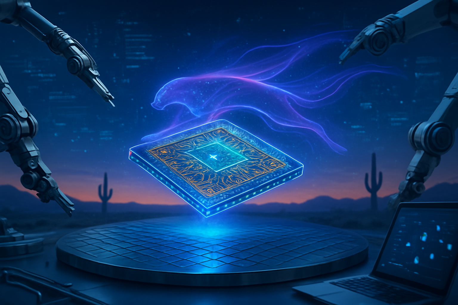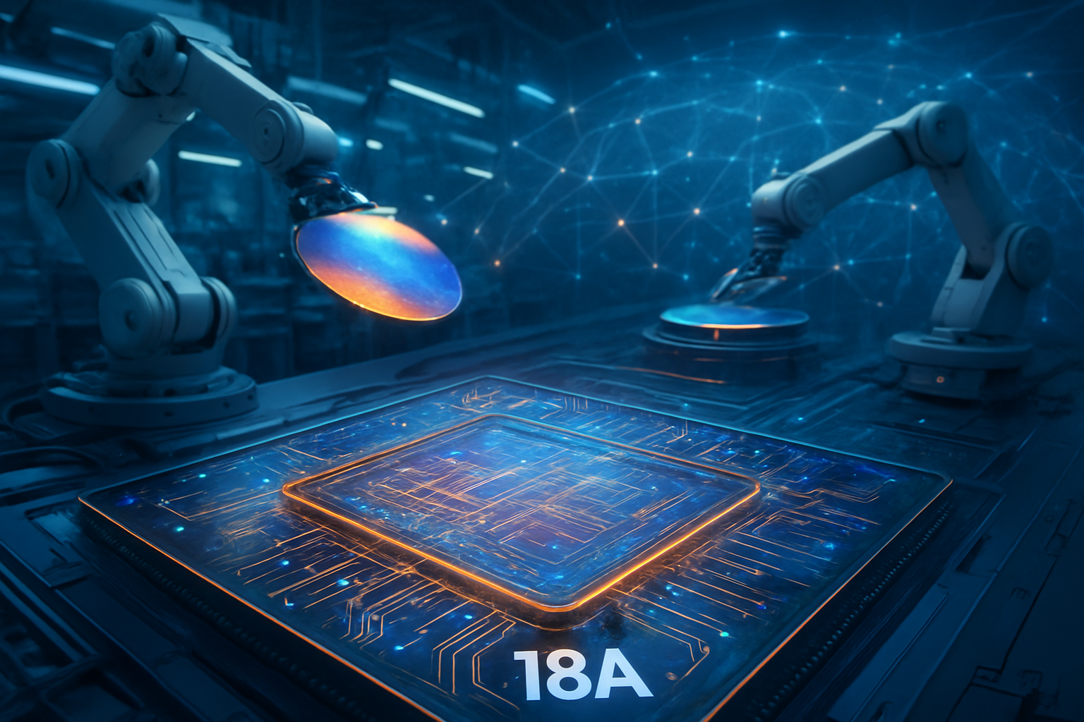
SANTA CLARA, Calif. — In a historic milestone for the American semiconductor industry, Intel (NASDAQ: INTC) has officially announced that its 18A (1.8nm-class) process node has entered high-volume manufacturing (HVM). The announcement, made during the opening keynote of CES 2026, marks the successful completion of the company’s ambitious "five nodes in four years" roadmap. For the first time in nearly a decade, Intel appears to have parity—and by some technical measures, a clear lead—over its primary rival, Taiwan Semiconductor Manufacturing Company (NYSE: TSM), in the race to power the next generation of artificial intelligence.
The immediate significance of 18A cannot be overstated. As AI models grow exponentially in complexity, the demand for chips that offer higher transistor density and significantly lower power consumption has reached a fever pitch. By reaching high-volume production with 18A, Intel is not just releasing a new processor; it is launching a fully-fledged foundry service capable of building the world’s most advanced AI accelerators for third-party clients. With anchor customers like Microsoft (NASDAQ: MSFT) and Amazon (NASDAQ: AMZN) already ramping up production on the node, the silicon landscape is undergoing its most radical shift since the invention of the integrated circuit.
The Architecture of Leadership: RibbonFET and PowerVia
The Intel 18A node represents a fundamental departure from the FinFET transistor architecture that has dominated the industry for over a decade. At the heart of 18A are two "world-first" technologies: RibbonFET and PowerVia. RibbonFET is Intel’s implementation of a Gate-All-Around (GAA) transistor, where the gate wraps entirely around the conducting channel. This provides superior electrostatic control, drastically reducing current leakage and allowing for higher drive currents at lower voltages. While TSMC (NYSE: TSM) has also moved to GAA with its N2 node, Intel’s 18A is distinguished by its integration of PowerVia—the industry’s first backside power delivery system.
PowerVia solves one of the most persistent bottlenecks in chip design: "voltage droop" and signal interference. In traditional chips, power and signal lines are intertwined on the front side of the wafer, competing for space. PowerVia moves the entire power delivery network to the back of the wafer, leaving the front exclusively for data signals. This separation allows for a 15% to 25% improvement in performance-per-watt and enables chips to run at higher clock speeds without overheating. Initial data from early 18A production runs indicates that Intel has achieved a transistor density of approximately 238 million transistors per square millimeter (MTr/mm²), providing a potent combination of raw speed and energy efficiency that is specifically tuned for AI workloads.
Industry experts have reacted with cautious optimism, noting that while TSMC’s N2 node still holds a slight lead in pure area density, Intel’s lead in backside power delivery gives it a strategic "performance-per-watt" advantage that is critical for massive data centers. "Intel has effectively leapfrogged the industry in power delivery architecture," noted one senior analyst at the event. "While the competition is still figuring out how to untangle their power lines, Intel is already shipping at scale."
A New Titan in the Foundry Market
The arrival of 18A transforms Intel Foundry from a theoretical competitor into a genuine threat to the TSMC-Samsung duopoly. By securing Microsoft (NASDAQ: MSFT) as a primary customer for its custom "Maia 2" AI accelerators, Intel has proven that its foundry model can attract the world’s largest "hyperscalers." Amazon (NASDAQ: AMZN) has similarly committed to 18A for its custom AI fabric and Graviton-series processors, seeking to reduce its reliance on external suppliers and optimize its internal cloud infrastructure for the generative AI era.
This development creates a complex competitive dynamic for AI leaders like NVIDIA (NASDAQ: NVDA). While NVIDIA remains heavily reliant on TSMC for its current H-series and B-series GPUs, the company reportedly made a strategic $5 billion investment in Intel’s advanced packaging capabilities in 2025. With 18A now in high-volume production, the industry is watching closely to see if NVIDIA will shift a portion of its next-generation "Rubin" or "Post-Rubin" architecture to Intel’s fabs to diversify its supply chain and hedge against geopolitical risks in the Taiwan Strait.
For startups and smaller AI labs, the emergence of a high-performance alternative in the United States could lower the barrier to entry for custom silicon. Intel’s "Secure Enclave" partnership with the U.S. Department of Defense further solidifies 18A as the premier node for sovereign AI applications, ensuring that the most sensitive government and defense chips are manufactured on American soil using the most advanced process technology available.
The Geopolitics of Silicon and the AI Landscape
The success of 18A is a pivotal moment for the broader AI landscape, which has been plagued by hardware shortages and energy constraints. As AI training clusters grow to consume hundreds of megawatts, the efficiency gains provided by PowerVia and RibbonFET are no longer just "nice-to-have" features—they are economic imperatives. Intel’s ability to deliver more "compute-per-watt" directly impacts the total cost of ownership for AI companies, potentially slowing the rise of energy costs associated with LLM (Large Language Model) development.
Furthermore, 18A represents the first major fruit of the CHIPS and Science Act, which funneled billions into domestic semiconductor manufacturing. The fact that this node is being produced at scale in Fab 52 in Chandler, Arizona, signals a shift in the global center of gravity for high-end manufacturing. It alleviates concerns about the "single point of failure" in the global AI supply chain, providing a robust, domestic alternative to East Asian foundries.
However, the transition is not without concerns. The complexity of 18A manufacturing is immense, and maintaining high yields at 1.8nm is a feat of engineering that requires constant vigilance. While current yields are reported in the 65%–75% range, any dip in production efficiency could lead to supply shortages or increased costs for customers. Comparisons to previous milestones, such as the transition to EUV (Extreme Ultraviolet) lithography, suggest that the first year of a new node is always a period of intense "learning by doing."
The Road to 14A and High-NA EUV
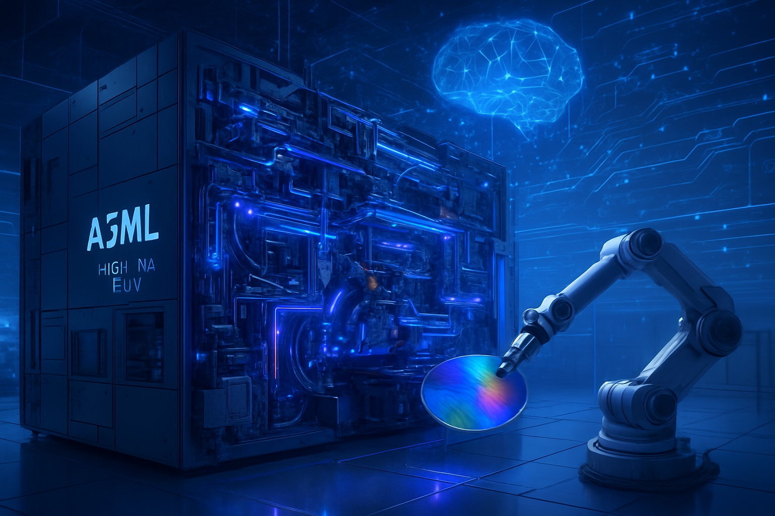
Looking ahead, Intel is already preparing the successor to 18A: the 14A (1.4nm) node. While 18A relies on standard 0.33 NA EUV lithography with multi-patterning, 14A will be the first node to fully utilize ASML (NASDAQ: ASML) High-NA (Numerical Aperture) EUV machines. Intel was the first in the industry to receive these "Twinscan EXE:5200" tools, and the company is currently using them for risk production and R&D to refine the 1.4nm process.
The near-term roadmap includes the launch of Intel’s "Panther Lake" mobile processors and "Clearwater Forest" server chips, both built on 18A. These products will serve as the "canary in the coal mine" for the node’s real-world performance. If Clearwater Forest, with its massive 288-core count, can deliver on its promised efficiency gains, it will likely trigger a wave of data center upgrades across the globe. Experts predict that by 2027, the industry will transition into the "Angstrom Era" entirely, where 18A and 14A become the baseline for all high-end AI and edge computing devices.
A Resurgent Intel in the AI History Books
The entry of Intel 18A into high-volume production is more than just a technical achievement; it is a corporate resurrection. After years of delays and lost leadership, Intel has successfully executed a "Manhattan Project" style turnaround. By betting early on backside power delivery and securing the world’s first High-NA EUV tools, Intel has positioned itself as the primary architect of the hardware that will define the late 2020s.
In the history of AI, the 18A node will likely be remembered as the point where hardware efficiency finally began to catch up with software ambition. The long-term impact will be felt in everything from the battery life of AI-integrated smartphones to the carbon footprint of massive neural network training runs. For the coming months, the industry will be watching yield reports and customer testimonials with intense scrutiny. If Intel can sustain this momentum, the "silicon crown" may stay in Santa Clara for a long time to come.
This content is intended for informational purposes only and represents analysis of current AI developments.
TokenRing AI delivers enterprise-grade solutions for multi-agent AI workflow orchestration, AI-powered development tools, and seamless remote collaboration platforms.
For more information, visit https://www.tokenring.ai/.