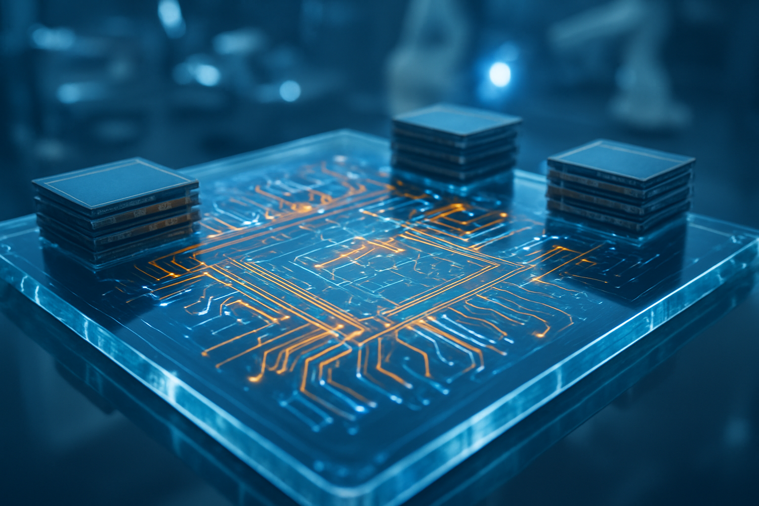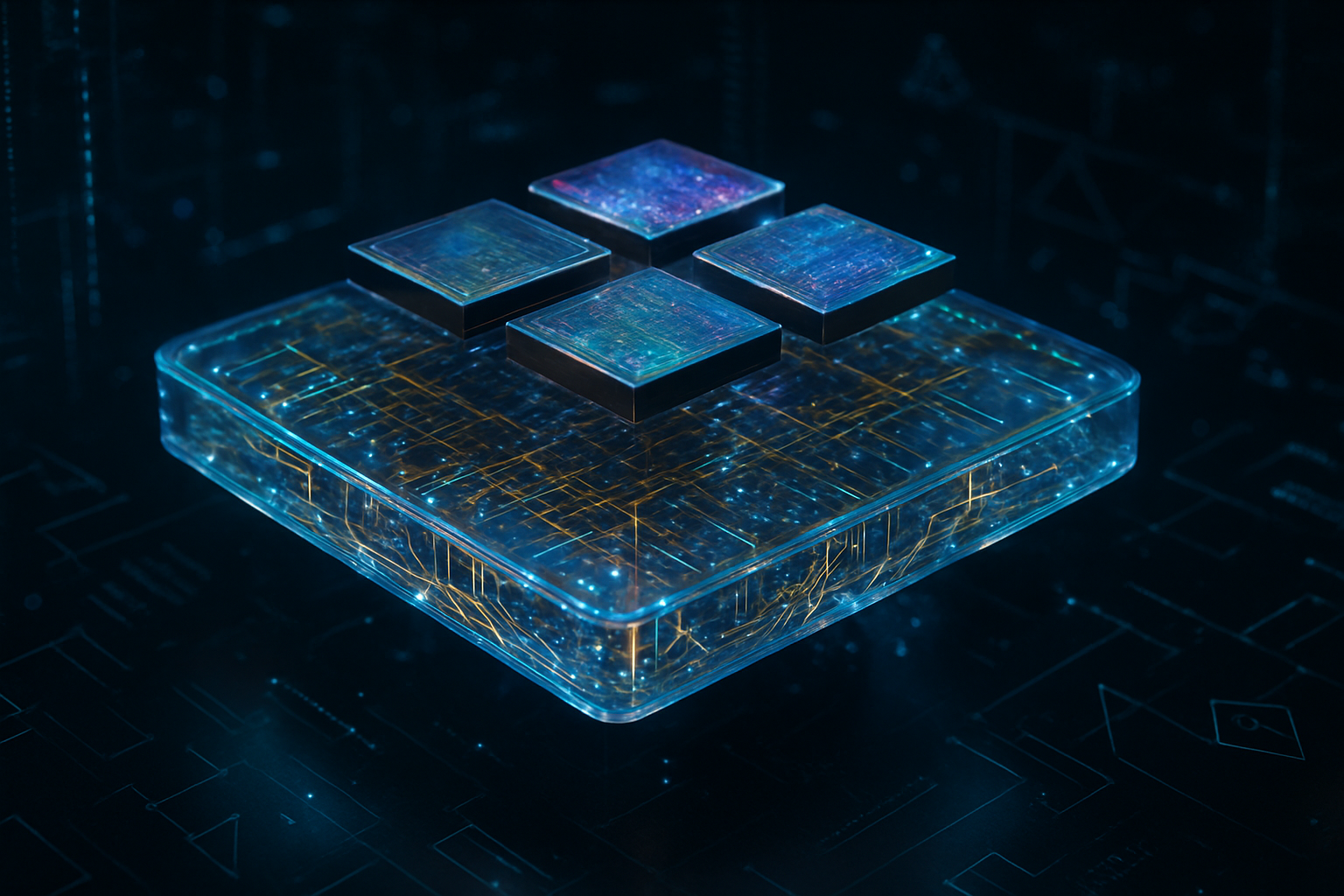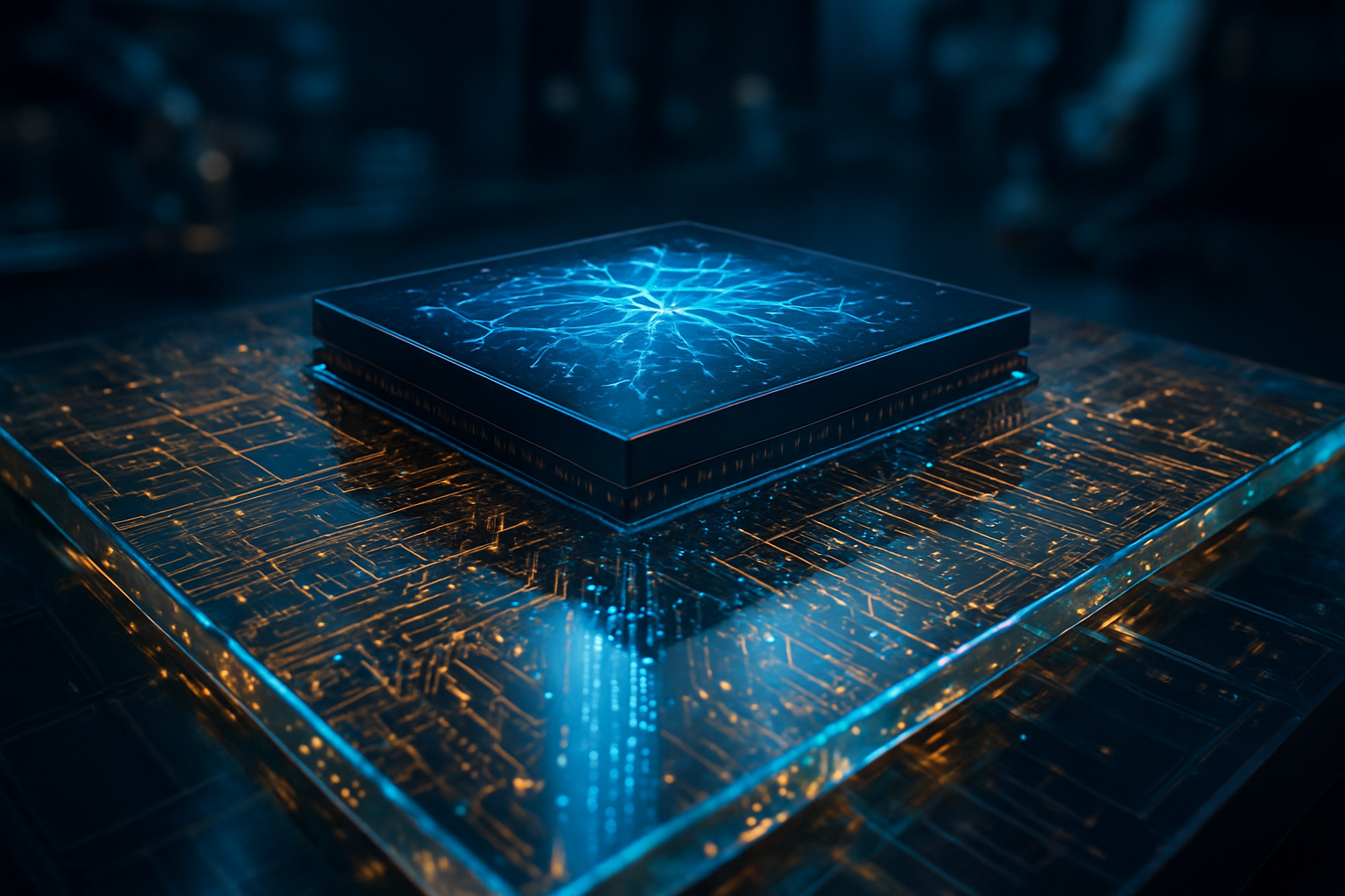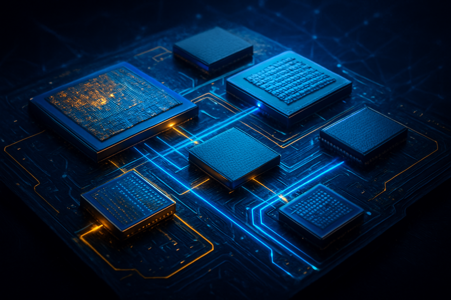
As the demand for artificial intelligence reaches an atmospheric peak, the semiconductor industry is undergoing its most radical transformation in decades. The era of the "monolithic" chip—a single, massive piece of silicon containing all a processor's functions—is rapidly coming to an end. In its place, a new paradigm of "chiplets" has emerged, where specialized pieces of silicon are mixed and matched like high-tech Lego bricks to create modular, hyper-efficient processors. This shift is being accelerated by the Universal Chiplet Interconnect Express (UCIe) standard, which has officially become the "universal language" of the silicon world, allowing components from different manufacturers to communicate with unprecedented speed and efficiency.
The immediate significance of this transition cannot be overstated. By breaking the physical and economic constraints of traditional chip manufacturing, chiplets are enabling the creation of AI accelerators that are ten times more powerful than the flagship models of just two years ago. For the first time, a single processor package can house specialized logic for generative AI, massive high-bandwidth memory, and high-speed networking components—all potentially sourced from different vendors but working as a unified whole.
The Architecture of Interoperability: Inside UCIe 3.0
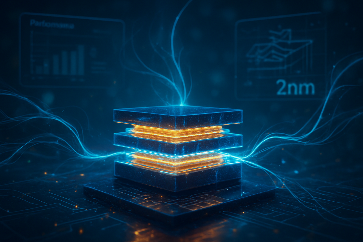
The technical backbone of this revolution is the UCIe 3.0 specification, which as of early 2026, has reached a level of maturity that makes multi-vendor silicon a commercial reality. Unlike previous proprietary interconnects, UCIe provides a standardized physical layer and protocol stack that enables data transfer at rates up to 64 GT/s. This allows for a staggering bandwidth density of up to 1.3 TB/s per shoreline millimeter in advanced packaging. Perhaps more importantly, the power efficiency of these links has plummeted to as low as 0.01 picojoules per bit (pJ/bit), meaning the energy cost of moving data between chiplets is now negligible compared to the energy used for computation.
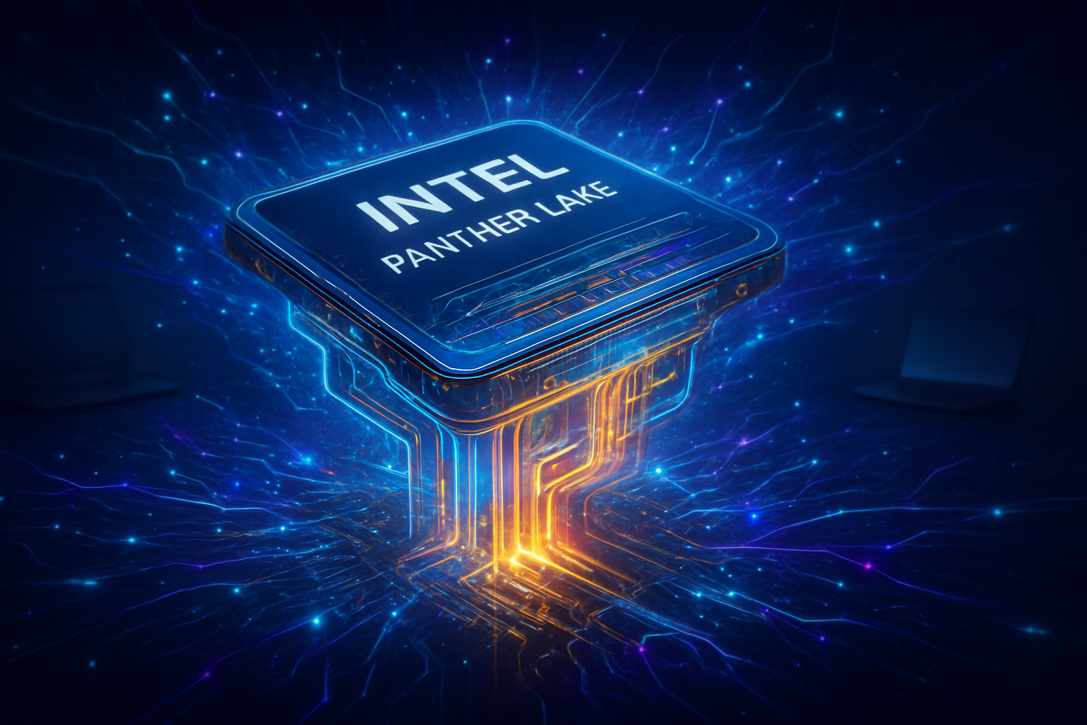
This modular approach differs fundamentally from the monolithic designs that dominated the last forty years. In a monolithic chip, every component must be manufactured on the same advanced (and expensive) process node, such as 2nm. With chiplets, designers can use the cutting-edge 2nm node for the critical AI compute cores while utilizing more mature, cost-effective 5nm or 7nm nodes for less sensitive components like I/O or power management. This "disaggregated" design philosophy is showcased in Intel's (NASDAQ: INTC) latest Panther Lake architecture and the Jaguar Shores AI accelerator, which utilize the company's 18A process for compute tiles while integrating third-party chiplets for specialized tasks.
Initial reactions from the AI research community have been overwhelmingly positive, particularly regarding the ability to scale beyond the "reticle limit." Traditional chips cannot be larger than the physical mask used in lithography (roughly 800mm²). Chiplet architectures, however, use advanced packaging techniques like TSMC’s (NYSE: TSM) CoWoS (Chip-on-Wafer-on-Substrate) to "stitch" multiple dies together, effectively creating processors that are twelve times the size of any possible monolithic chip. This has paved the way for the massive GPU clusters required for training the next generation of trillion-parameter large language models (LLMs).
Strategic Realignment: The Battle for the Modular Crown
The rise of chiplets has fundamentally altered the competitive landscape for tech giants and startups alike. AMD (NASDAQ: AMD) has leveraged its early lead in chiplet technology to launch the Instinct MI400 series, the industry’s first GPU to utilize 2nm compute chiplets alongside HBM4 memory. By perfecting the "Venice" EPYC CPU and MI400 GPU synergy, AMD has positioned itself as the primary alternative to NVIDIA (NASDAQ: NVDA) for enterprise-scale AI. Meanwhile, NVIDIA has responded with its Rubin platform, confirming that while it still favors its proprietary NVLink-C2C for internal "superchips," it is a lead promoter of UCIe to ensure its hardware can integrate into the increasingly modular data centers of the future.
This development is a massive boon for "Hyperscalers" like Microsoft (NASDAQ: MSFT), Alphabet (NASDAQ: GOOGL), and Amazon (NASDAQ: AMZN). These companies are now designing their own custom AI ASICs (Application-Specific Integrated Circuits) that incorporate their proprietary logic alongside off-the-shelf chiplets from ARM (NASDAQ: ARM) or specialized startups. This "mix-and-match" capability reduces their reliance on any single chip vendor and allows them to tailor hardware specifically to their proprietary AI workloads, such as Gemini or Azure AI services.
The disruption extends to the foundry business as well. TSMC remains the dominant player due to its advanced packaging capacity, which is projected to reach 130,000 wafers per month by the end of 2026. However, Samsung (KRX: 005930) is mounting a significant challenge with its "turnkey" service, offering HBM4, foundry services, and its I-Cube packaging under one roof. This competition is driving down costs for AI startups, who can now afford to tape out smaller, specialized chiplets rather than betting their entire venture on a single, massive monolithic design.
Beyond Moore’s Law: The Economic and Technical Significance
The shift to chiplets represents a critical evolution in the face of the slowing of Moore’s Law. As it becomes exponentially more difficult and expensive to shrink transistors, the industry has turned to "system-level" scaling. The economic implications are profound: smaller chiplets yield significantly better than large dies. If a single defect occurs on a massive monolithic wafer, the entire chip is scrapped; if a defect occurs on a small chiplet, only that tiny piece of silicon is lost. This yield improvement is what has allowed AI hardware prices to remain relatively stable despite the soaring costs of 2nm and 1.8nm manufacturing.
Furthermore, the "Lego-ification" of silicon is democratizing high-performance computing. Specialized firms like Ayar Labs and Lightmatter are now producing UCIe-compliant optical I/O chiplets. These can be dropped into an existing processor package to replace traditional copper wiring with light-based communication, solving the thermal and bandwidth bottlenecks that have long plagued AI clusters. This level of modular innovation was impossible when every component had to be designed and manufactured by a single entity.
However, this new era is not without its concerns. The complexity of testing and validating a "system-in-package" (SiP) that contains silicon from four different vendors is immense. There are also rising concerns about "thermal hotspots," as stacking chiplets vertically (3D packaging) makes it harder to dissipate heat. The industry is currently racing to develop standardized liquid cooling and "through-silicon via" (TSV) technologies to address these physical limitations.
The Horizon: 3D Stacking and Software-Defined Silicon
Looking forward, the next frontier is true 3D integration. While current designs largely rely on 2.5D packaging (placing chiplets side-by-side on a base layer), the industry is moving toward hybrid bonding. This will allow chiplets to be stacked directly on top of one another with micron-level precision, enabling thousands of vertical connections. Experts predict that by 2027, we will see "memory-on-logic" stacks where HBM4 is bonded directly to the AI compute cores, virtually eliminating the latency that currently slows down inference tasks.
Another emerging trend is "software-defined silicon." With the UCIe 3.0 manageability system architecture, developers can dynamically reconfigure how chiplets interact based on the specific AI model being run. A chip could, for instance, prioritize low-precision FP4 math for a fast-response chatbot in the morning and reconfigure its interconnects for high-precision FP64 scientific simulations in the afternoon.
The primary challenge remaining is the software stack. Ensuring that compilers and operating systems can efficiently distribute workloads across a heterogeneous collection of chiplets is a monumental task. Companies like Tenstorrent are leading the way with RISC-V based modular designs, but a unified software standard to match the UCIe hardware standard is still in its infancy.
A New Era for Computing
The rise of chiplets and the UCIe standard marks the end of the "one-size-fits-all" era of semiconductor design. We have moved from a world of monolithic giants to a collaborative ecosystem of specialized components. This shift has not only saved Moore’s Law from obsolescence but has provided the necessary hardware foundation for the AI revolution to continue its exponential growth.
As we move through 2026, the industry will be watching for the first truly "heterogeneous" commercial processors—chips that combine an Intel CPU, an NVIDIA-designed AI accelerator, and a third-party networking chiplet in a single package. The technical hurdles are significant, but the economic and performance incentives are now too great to ignore. The silicon mosaic is here, and it is the most important development in computer architecture since the invention of the integrated circuit itself.
This content is intended for informational purposes only and represents analysis of current AI developments.
TokenRing AI delivers enterprise-grade solutions for multi-agent AI workflow orchestration, AI-powered development tools, and seamless remote collaboration platforms.
For more information, visit https://www.tokenring.ai/.