As of early 2026, the semiconductor industry has reached a historic inflection point where the traditional method of scaling transistors—shrinking them to pack more onto a single piece of silicon—has effectively hit a physical and economic wall. In its place, a new frontier has emerged: advanced packaging. No longer a mere "back-end" process for protecting chips, advanced packaging has become the primary engine of AI performance, enabling the massive computational leaps required for the next generation of generative AI and sovereign AI clouds.
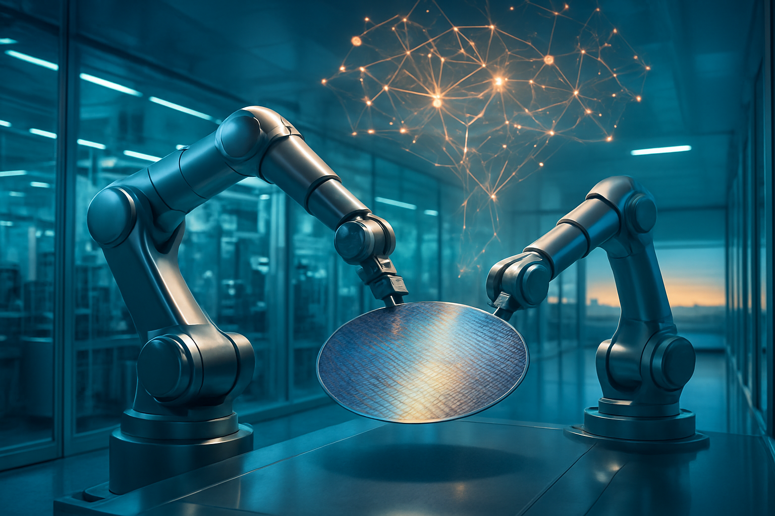
The immediate significance of this shift is visible in the latest hardware architectures from industry leaders. By moving away from monolithic designs toward heterogeneous "chiplets" connected through 3D stacking and hybrid bonding, manufacturers are bypassing the "reticle limit"—the maximum size a single chip can be—to create massive "systems-in-package" (SiP). This transition is not just a technical evolution; it is a total restructuring of the semiconductor supply chain, shifting the industry's profit centers and geopolitical focus toward the complex assembly of silicon.
The Technical Frontier: Hybrid Bonding and the HBM4 Breakthrough
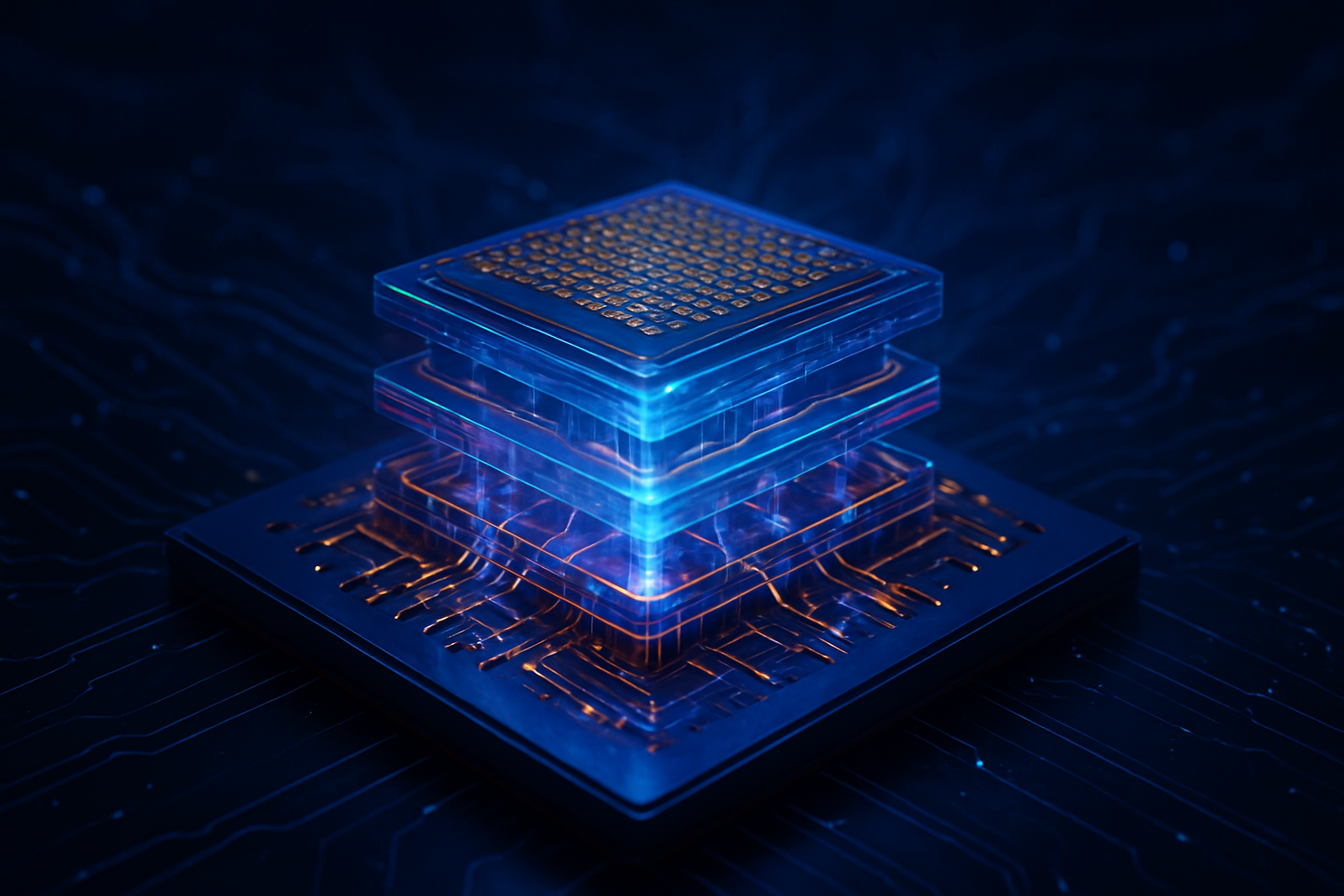
The technical cornerstone of the 2026 AI chip landscape is the mass adoption of hybrid bonding, specifically TSMC (NYSE: TSM) System on Integrated Chips (SoIC). Unlike traditional packaging that uses tiny solder balls (micro-bumps) to connect chips, hybrid bonding uses direct copper-to-copper connections. In early 2026, commercial bond pitches have reached a staggering 6 micrometers (µm), providing a 15x increase in interconnect density over previous generations. This "bumpless" architecture reduces the vertical distance between logic and memory to mere microns, slashing latency by 40% and drastically improving energy efficiency.
Simultaneously, the arrival of HBM4 (High Bandwidth Memory 4) has shattered the "memory wall" that plagued 2024-era AI accelerators. HBM4 doubles the memory interface width from 1024-bit to 2048-bit, allowing bandwidths to exceed 2.0 TB/s per stack. Leading memory makers like SK Hynix and Samsung (KRX: 005930) are now shipping 12-layer and 16-layer stacks thinned to just 30 micrometers—roughly one-third the thickness of a human hair. For the first time, the base die of these memory stacks is being manufactured on advanced logic nodes (5nm), allowing them to be bonded directly on top of GPU logic via hybrid bonding, creating a true 3D compute sandwich.
Industry experts and researchers have reacted with awe at the performance benchmarks of these 3D-stacked "monsters." NVIDIA (NASDAQ: NVDA) recently debuted its Rubin R100 architecture, which utilizes these 3D techniques to deliver a 4x performance-per-watt improvement over the Blackwell series. The consensus among the research community is that we have entered the "Packaging-First" era, where the design of the interconnects is now as critical as the design of the transistors themselves.
The Business Pivot: Profit Margins Migrate to the Package
The economic landscape of the semiconductor industry is undergoing a fundamental transformation as profitability migrates from logic manufacturing to advanced packaging. Leading-edge packaging services, such as TSMC’s CoWoS-L (Chip-on-Wafer-on-Substrate), now command gross margins of 65% to 70%, significantly higher than the typical margins for standard wafer fabrication. This "bottleneck premium" reflects the reality that advanced packaging is now the final gatekeeper of AI hardware supply.
TSMC remains the undisputed leader, with its advanced packaging revenue expected to reach $18 billion in 2026, nearly 10% of its total revenue. However, the competition is intensifying. Intel (NASDAQ: INTC) is aggressively ramping its Fab 52 in Arizona to provide Foveros 3D packaging services to external customers, positioning itself as a domestic alternative for Western tech giants like Amazon (NASDAQ: AMZN) and Microsoft (NASDAQ: MSFT). Meanwhile, Samsung has unified its memory and foundry divisions to offer a "one-stop-shop" for HBM4 and logic integration, aiming to reclaim market share lost during the HBM3e era.
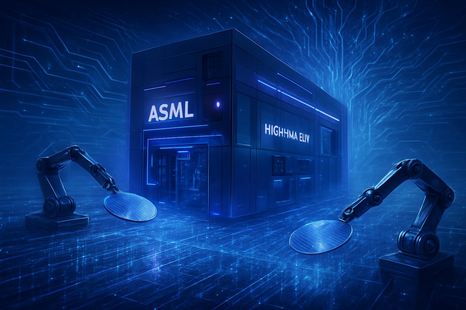
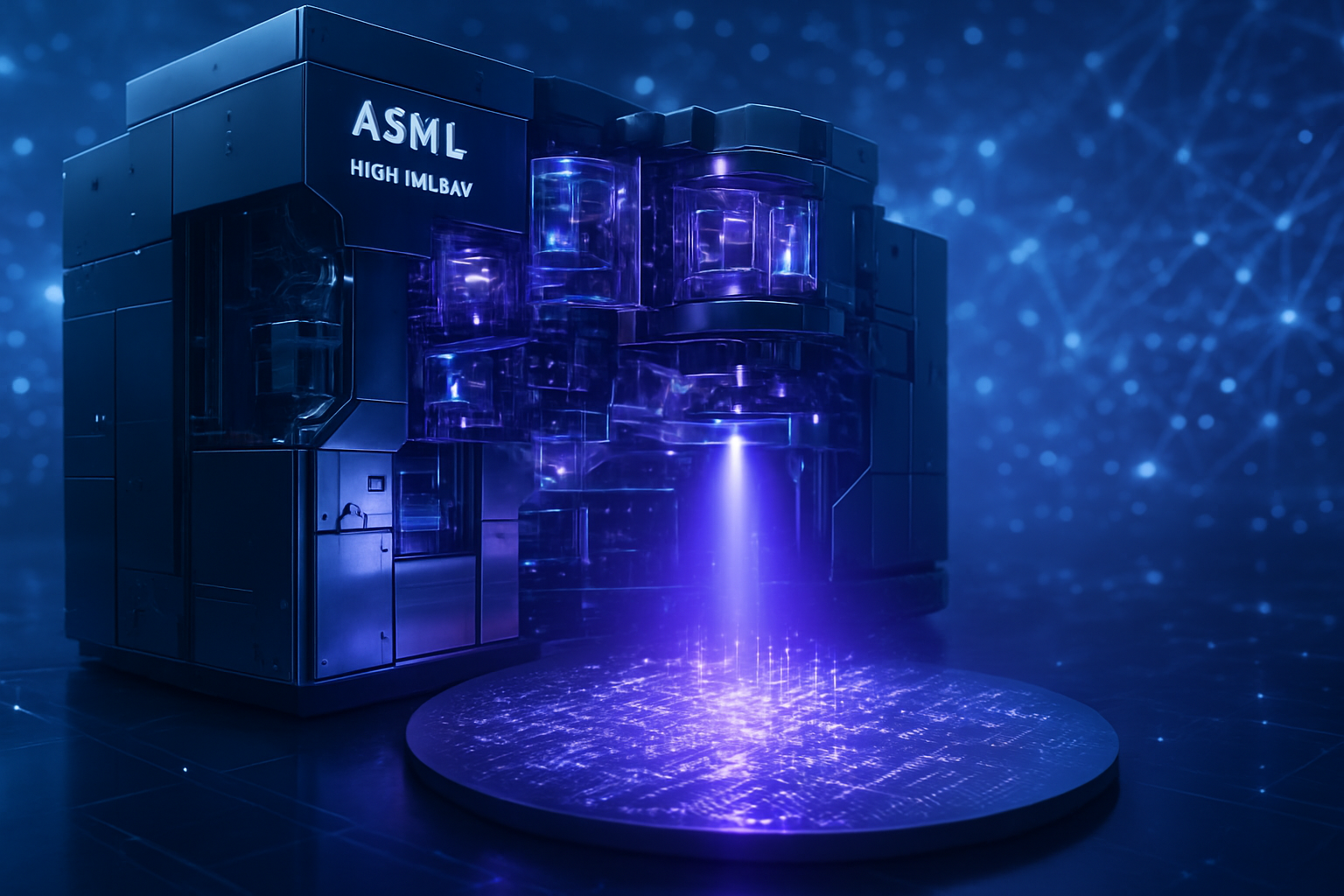
This shift also benefits a specialized ecosystem of equipment and service providers. Companies like ASML (NASDAQ: ASML) have introduced new i-line scanners specifically designed for 3D integration, while Besi and Applied Materials (NASDAQ: AMAT) have formed a strategic alliance to dominate the hybrid bonding equipment market. Outsourced Semiconductor Assembly and Test (OSAT) giants like ASE Technology (NYSE: ASX) and Amkor (NASDAQ: AMKR) are also seeing record backlogs as they handle the "overflow" of advanced packaging orders that the major foundries cannot fulfill.
Geopolitics and the Wider Significance of the Packaging Wall
Beyond the balance sheets, advanced packaging has become a central pillar of national security and geopolitical strategy. The U.S. CHIPS Act has funneled billions into domestic packaging initiatives, recognizing that while the U.S. designs the world's best AI chips, the "last mile" of manufacturing has historically been concentrated in Asia. The National Advanced Packaging Manufacturing Program (NAPMP) has awarded $1.4 billion to secure an end-to-end U.S. supply chain, including Amkor’s massive $7 billion facility in Arizona and SK Hynix’s $3.9 billion HBM plant in Indiana.
However, the move to 3D-stacked AI chips comes with a heavy environmental price tag. The complexity of these manufacturing processes has led to a projected 16-fold increase in CO2e emissions from GPU manufacturing between 2024 and 2030. Furthermore, the massive power draw of these chips—often exceeding 1,000W per module—is pushing data centers to their limits. This has sparked a secondary boom in liquid cooling infrastructure, as air cooling is no longer sufficient to dissipate the heat generated by 3D-stacked silicon.
In the broader context of AI history, this transition is comparable to the shift from planar transistors to FinFETs or the introduction of Extreme Ultraviolet (EUV) lithography. It represents a "re-architecting" of the computer itself. By breaking the monolithic chip into specialized chiplets, the industry is creating a modular ecosystem where different components can be optimized for specific tasks, effectively extending the life of Moore's Law through clever geometry rather than just smaller features.
The Horizon: Glass Substrates and Optical Everything
Looking toward the late 2020s, the roadmap for advanced packaging points toward even more exotic materials and technologies. One of the most anticipated developments is the transition to glass substrates. Leading players like Intel and Samsung are preparing to replace traditional organic substrates with glass, which offers superior flatness and thermal stability. Glass substrates will enable 10x higher routing density and allow for massive "System-on-Wafer" designs that could integrate dozens of chiplets into a single, dinner-plate-sized processor by 2027.
The industry is also racing toward "Optical Everything." Co-Packaged Optics (CPO) and Silicon Photonics are expected to hit a major inflection point by late 2026. By replacing electrical copper links with light-based communication directly on the chip package, manufacturers can reduce I/O power consumption by 50% while breaking the bandwidth barriers that currently limit multi-GPU clusters. This will be essential for training the "Frontier Models" of 2027, which are expected to require tens of thousands of interconnected GPUs working as a single unified machine.
The design of these incredibly complex packages is also being revolutionized by AI itself. Electronic Design Automation (EDA) leaders like Synopsys (NASDAQ: SNPS) and Cadence (NASDAQ: CDNS) have integrated generative AI into their tools to solve "multi-physics" problems—simultaneously optimizing for heat, electricity, and mechanical stress. These AI-driven tools are compressing design timelines from months to weeks, allowing chip designers to iterate at the speed of the AI software they are building for.
Final Assessment: The Era of Silicon Integration
The rise of advanced packaging marks the end of the "Scaling Era" and the beginning of the "Integration Era." In this new paradigm, the value of a chip is determined not just by how many transistors it has, but by how efficiently those transistors can communicate with memory and other processors. The breakthroughs in hybrid bonding and 3D stacking seen in early 2026 have successfully averted a stagnation in AI performance, ensuring that the trajectory of artificial intelligence remains on its exponential path.
As we move forward, the key metrics to watch will be HBM4 yield rates and the successful deployment of domestic packaging facilities in the United States and Europe. The "Packaging Wall" was once seen as a threat to the industry's progress; today, it has become the foundation upon which the next decade of AI innovation will be built. For the tech industry, the message is clear: the future of AI isn't just about what's inside the chip—it's about how you put the pieces together.
This content is intended for informational purposes only and represents analysis of current AI developments.
TokenRing AI delivers enterprise-grade solutions for multi-agent AI workflow orchestration, AI-powered development tools, and seamless remote collaboration platforms.
For more information, visit https://www.tokenring.ai/.