As of January 2, 2026, the global semiconductor industry has officially entered what analysts are calling the "Silicon Super-Cycle." Following a record-breaking 2025 that saw industry revenues soar past $800 billion, new data suggests the sector is now on an irreversible trajectory to exceed $1 trillion in annual revenue by 2030. This monumental growth is no longer speculative; it is being cemented by the relentless expansion of generative AI infrastructure, the total electrification of the automotive sector, and a new generation of "Agentic" IoT devices that require unprecedented levels of on-device intelligence.
The significance of this milestone cannot be overstated. For decades, the semiconductor market was defined by cyclical booms and busts tied to PC and smartphone demand. However, the current era represents a structural shift where silicon has become the foundational commodity of the global economy—as essential as oil was in the 20th century. With the industry growing at a compound annual growth rate (CAGR) of over 8%, the race to $1 trillion is being led by a handful of titans who are redefining the limits of physics and manufacturing.
The Technical Engine: 2nm, 18A, and the Rubin Revolution
The technical landscape of 2026 is dominated by a fundamental shift in transistor architecture. For the first time in over a decade, the industry has moved away from the FinFET (Fin Field-Effect Transistor) design that powered the previous generation of electronics. Taiwan Semiconductor Manufacturing Company (NYSE: TSM), commonly known as TSMC, has successfully ramped up its 2nm (N2) process, utilizing Nanosheet Gate-All-Around (GAA) transistors. This transition allows for a 15% performance boost or a 30% reduction in power consumption compared to the 3nm nodes of 2024.
Simultaneously, Intel (NASDAQ: INTC) has achieved a major milestone with its 18A (1.8nm) process, which entered high-volume production at its Arizona facilities this month. The 18A node introduces "PowerVia," the industry’s first implementation of backside power delivery, which separates the power lines from the data lines on a chip to reduce interference and improve efficiency. This technical leap has allowed Intel to secure major foundry customers, including a landmark partnership with NVIDIA (NASDAQ: NVDA) for specialized AI components.
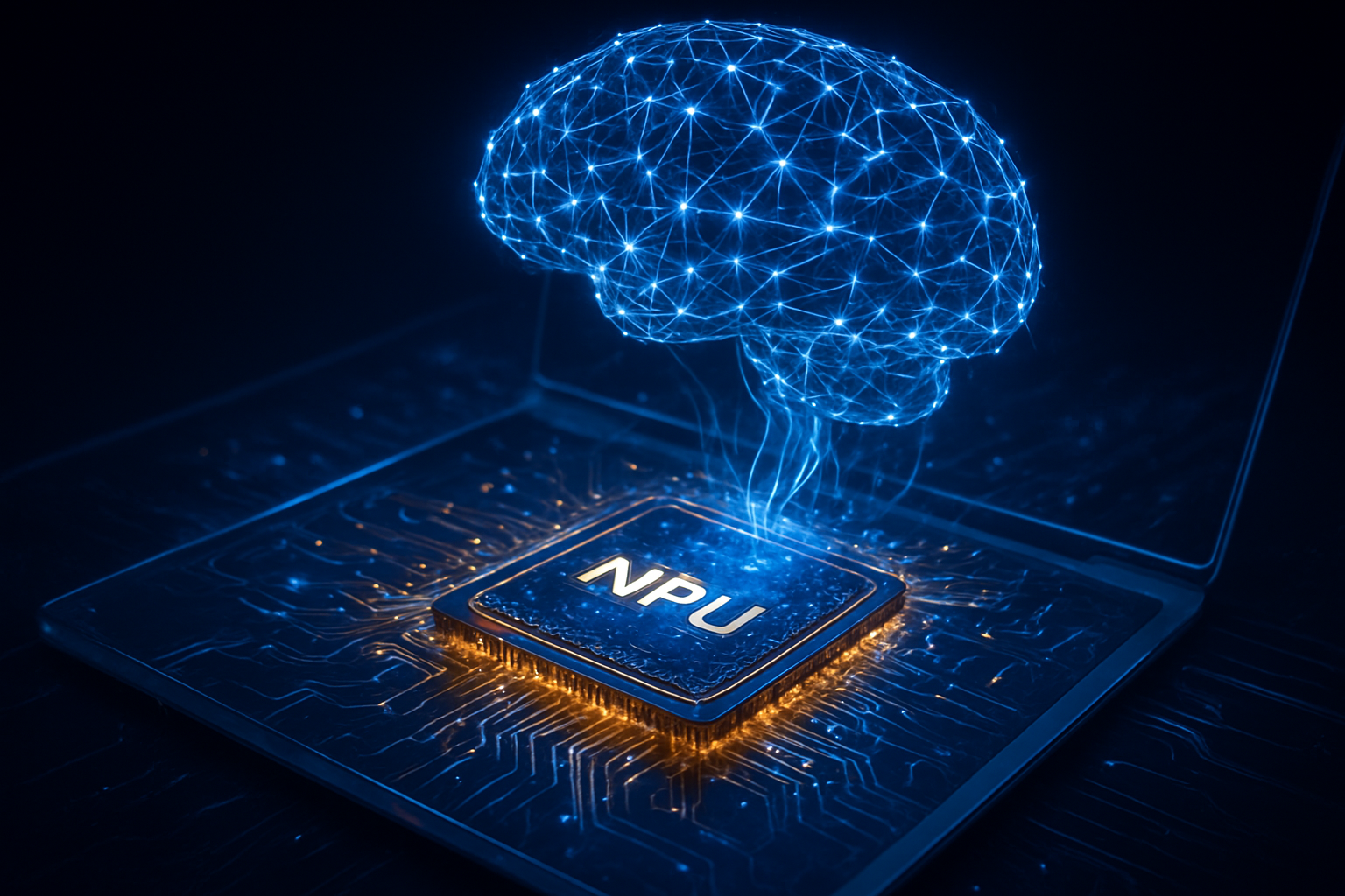
On the architectural front, NVIDIA has just begun shipping its "Rubin" R100 GPUs, the successor to the Blackwell line. The Rubin architecture is the first to fully integrate the HBM4 (High Bandwidth Memory 4) standard, which doubles the memory bus width to 2048-bit and provides a staggering 2.0 TB/s of peak throughput per stack. This leap in memory performance is critical for "Agentic AI"—autonomous AI systems that require massive local memory to process complex reasoning tasks in real-time without constant cloud polling.
The Beneficiaries: NVIDIA’s Dominance and the Foundry Wars
The primary beneficiary of this $1 trillion march remains NVIDIA, which briefly touched a $5 trillion market capitalization in late 2025. By controlling over 90% of the AI accelerator market, NVIDIA has effectively become the gatekeeper of the AI era. However, the competitive landscape is shifting. Advanced Micro Devices (NASDAQ: AMD) has gained significant ground with its MI400 series, capturing nearly 15% of the data center market by offering a more open software ecosystem compared to NVIDIA’s proprietary CUDA platform.
The "Foundry Wars" have also intensified. While TSMC still holds a dominant 70% market share, the resurgence of Intel Foundry and the steady progress of Samsung (KRX: 005930) have created a more fragmented market. Samsung recently secured a $16.5 billion deal with Tesla (NASDAQ: TSLA) to produce next-generation Full Self-Driving (FSD) chips using its 3nm GAA process. Meanwhile, Broadcom (NASDAQ: AVGO) and Marvell (NASDAQ: MRVL) are seeing record revenues as "hyperscalers" like Google and Amazon shift toward custom-designed AI ASICs (Application-Specific Integrated Circuits) to reduce their reliance on off-the-shelf GPUs.
This shift toward customization is disrupting the traditional "one-size-fits-all" chip model. Startups specializing in "Edge AI" are finding fertile ground as the market moves from training large models in the cloud to running them on local devices. Companies that can provide high-performance, low-power silicon for the "Intelligence of Things" are increasingly becoming acquisition targets for tech giants looking to vertically integrate their hardware stacks.
The Global Stakes: Geopolitics and the Environmental Toll
As the semiconductor industry scales toward $1 trillion, it has become the primary theater of global geopolitical competition. The U.S. CHIPS Act has transitioned from a funding phase to an operational one, with several leading-edge "mega-fabs" now online in the United States. This has created a strategic buffer, yet the world remains heavily dependent on the "Silicon Shield" of Taiwan. In late 2025, simulated blockades in the Taiwan Strait sent shockwaves through the market, highlighting that even a minor disruption in the region could risk a $500 billion hit to the global economy.
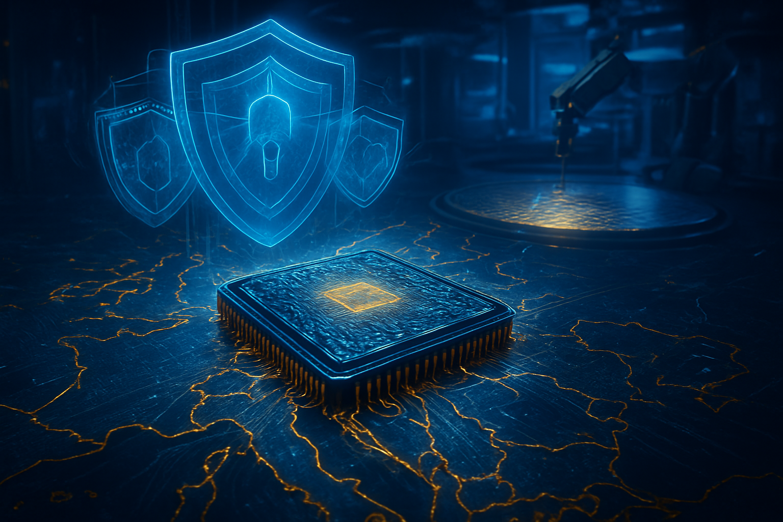
Beyond geopolitics, the environmental impact of a $1 trillion industry is coming under intense scrutiny. A single modern mega-fab in 2026 consumes as much as 10 million gallons of ultrapure water per day and requires energy levels equivalent to a small city. The transition to 2nm and 1.8nm nodes has increased energy intensity by nearly 3.5x compared to legacy nodes. In response, the industry is pivoting toward "Circular Silicon" initiatives, with TSMC and Intel pledging to recycle 85% of their water and transition to 100% renewable energy by 2030 to mitigate regulatory pressure and resource scarcity.
This environmental friction is a new phenomenon for the industry. Unlike the software booms of the past, the semiconductor super-cycle is tied to physical constraints—land, water, power, and rare earth minerals. The ability of a company to secure "green" manufacturing capacity is becoming as much of a competitive advantage as the transistor density of its chips.
The Road to 2030: Edge AI and the Intelligence of Things
Looking ahead, the next four years will be defined by the migration of AI from the data center to the "Edge." While the current revenue surge is driven by massive server farms, the path to $1 trillion will be paved by the billions of devices in our pockets, homes, and cars. We are entering the era of the "Intelligence of Things" (IoT 2.0), where every sensor and appliance will possess enough local compute power to run sophisticated AI agents.
In the automotive sector, the semiconductor content per vehicle is expected to double by 2030. Modern Electric Vehicles (EVs) are essentially data centers on wheels, requiring high-power silicon carbide (SiC) semiconductors for power management and high-end SoCs (System on a Chip) for autonomous navigation. Qualcomm (NASDAQ: QCOM) is positioning itself as a leader in this space, leveraging its mobile expertise to dominate the "Digital Cockpit" market.
Experts predict that the next major breakthrough will involve Silicon Photonics—using light instead of electricity to move data between chips. This technology, expected to hit the mainstream by 2028, could solve the "interconnect bottleneck" that currently limits the scale of AI clusters. As we approach the end of the decade, the integration of quantum-classical hybrid chips is also expected to emerge, providing a new frontier for specialized scientific computing.
A New Industrial Bedrock
The semiconductor industry's journey to $1 trillion is a testament to the central role of hardware in the AI revolution. The key takeaway from early 2026 is that the industry has successfully navigated the transition to GAA transistors and localized manufacturing, creating a more resilient, albeit more expensive, global supply chain. The "Silicon Super-Cycle" is no longer just about faster computers; it is about the infrastructure of modern life.
In the history of technology, this period will likely be remembered as the moment semiconductors surpassed the automotive and energy industries in strategic importance. The long-term impact will be a world where intelligence is "baked in" to every physical object, driven by the chips currently rolling off the assembly lines in Hsinchu, Phoenix, and Magdeburg.
In the coming weeks and months, investors and industry watchers should keep a eye on the yield rates of 2nm production and the first real-world benchmarks of NVIDIA’s Rubin GPUs. These metrics will determine which companies will capture the lion's share of the final $200 billion climb to the trillion-dollar mark.
This content is intended for informational purposes only and represents analysis of current AI developments.
TokenRing AI delivers enterprise-grade solutions for multi-agent AI workflow orchestration, AI-powered development tools, and seamless remote collaboration platforms.
For more information, visit https://www.tokenring.ai/.