The semiconductor industry has reached its most significant architectural milestone in over a decade. As of January 2, 2026, the transition from the long-standing FinFET (Fin Field-Effect Transistor) design to the revolutionary Nanosheet, or Gate-All-Around (GAA), architecture is no longer a roadmap projection—it is a commercial reality. Leading the charge are Taiwan Semiconductor Manufacturing Company (NYSE: TSM) and Intel Corporation (NASDAQ: INTC), both of which have successfully moved their 2nm-class nodes into high-volume manufacturing to meet the insatiable computational demands of the global AI boom.
This shift represents more than just a routine shrink in transistor size; it is a fundamental reimagining of how electricity is controlled at the atomic level. By surrounding the transistor channel on all four sides with the gate, GAA architecture virtually eliminates the power leakage that has plagued the industry at the 3nm limit. For the world’s leading AI labs and hardware designers, this breakthrough provides the essential "thermal headroom" required to scale the next generation of Large Language Models (LLMs) and autonomous systems, effectively bypassing the "power wall" that threatened to stall AI progress.
The Technical Foundation: Atomic Control and the Death of Leakage
The move to Nanosheet GAA is the first major structural change in transistor design since the industry adopted FinFET in 2011. In a FinFET structure, the gate wraps around three sides of a vertical "fin" channel. While effective for over a decade, as features shrank toward 3nm, the bottom of the fin remained exposed, allowing sub-threshold leakage—electricity that flows even when the transistor is "off." This leakage generates heat and wastes power, a critical bottleneck for data centers running thousands of interconnected GPUs.
Nanosheet GAA solves this by stacking horizontal sheets of silicon and wrapping the gate entirely around them on all four sides. This "Gate-All-Around" configuration provides superior electrostatic control, allowing for faster switching speeds and significantly lower power consumption. Furthermore, GAA introduces "width scalability." Unlike FinFETs, where designers could only increase drive current by adding more discrete fins, nanosheet widths can be continuously adjusted. This allows engineers to fine-tune each transistor for either maximum performance or minimum power, providing a level of design flexibility previously thought impossible.
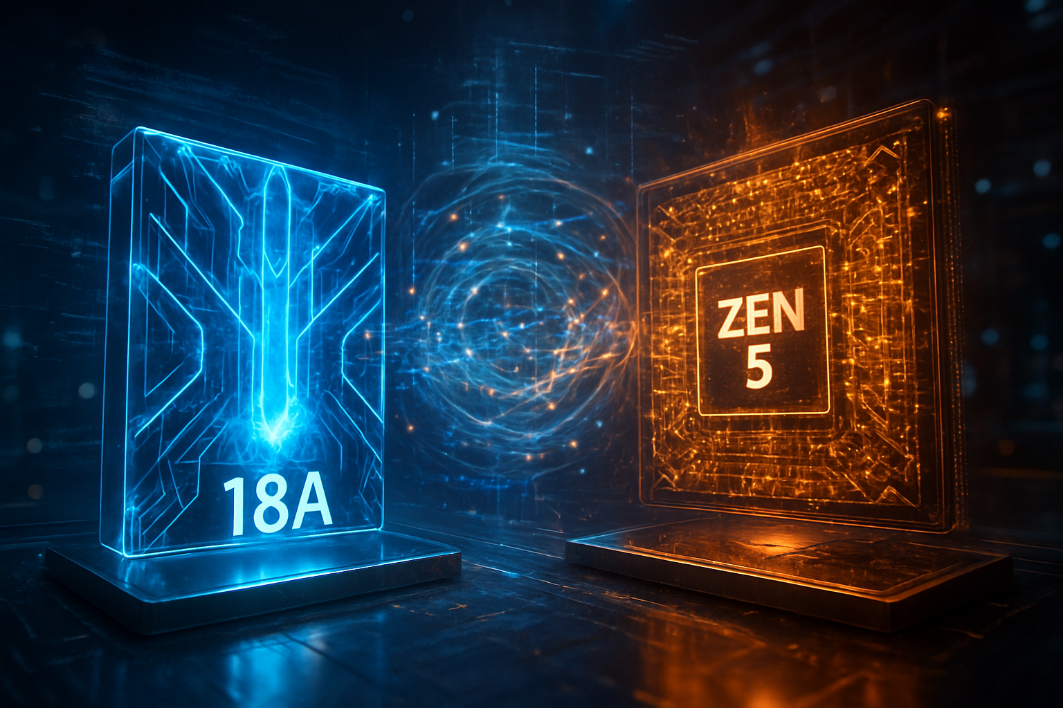
Complementing the GAA transition is the introduction of Backside Power Delivery (BSPDN). Intel (NASDAQ: INTC) has pioneered this with its "PowerVia" technology on the 18A node, while TSMC (NYSE: TSM) is integrating its "SuperPowerRail" in its refined 2nm processes. By moving the power delivery network to the back of the wafer and leaving the front exclusively for signal interconnects, manufacturers can reduce voltage drop and free up more space for transistors. Initial industry reports suggest that the combination of GAA and BSPDN results in a 30% reduction in power consumption at the same performance levels compared to 3nm FinFET chips.
Strategic Realignment: The "Silicon Elite" and the 2nm Race
The high cost and complexity of 2nm GAA manufacturing have created a widening gap between the "Silicon Elite" and the rest of the industry. Apple (NASDAQ: AAPL) remains the primary driver for TSMC’s N2 node, securing the vast majority of initial capacity for its A19 Pro and M5 chips. Meanwhile, Nvidia (NASDAQ: NVDA) is expected to leverage these efficiency gains for its upcoming "Rubin" GPU architecture, which aims to provide a 4x increase in inference performance while keeping power draw within the manageable 1,000W-to-1,500W per-rack envelope.
Intel’s successful ramp of its 18A node marks a pivotal moment for the company’s "five nodes in four years" strategy. By reaching manufacturing readiness in early 2026, Intel has positioned itself as a viable alternative to TSMC for external foundry customers. Microsoft (NASDAQ: MSFT) and various government agencies have already signed on as lead customers for 18A, seeking to secure a domestic supply of cutting-edge AI silicon. This competitive pressure has forced Samsung Electronics (KOSPI: 005930) to accelerate its own Multi-Bridge Channel FET (MBCFET) roadmap, targeting Japanese AI startups and mobile chip designers like Qualcomm (NASDAQ: QCOM) to regain lost market share.
For the broader tech ecosystem, the transition to GAA is disruptive. Traditional chip designers who cannot afford the multi-billion dollar design costs of 2nm are increasingly turning to "chiplet" architectures, where they combine older, cheaper 5nm or 7nm components with a single, high-performance 2nm "compute tile." This modular approach is becoming the standard for startups and mid-tier AI companies, allowing them to benefit from GAA efficiency without the prohibitive entry costs of a monolithic 2nm design.
The Global Stakes: Sustainability and Silicon Sovereignty
The significance of the Nanosheet revolution extends far beyond the laboratory. In the broader AI landscape, energy efficiency is now the primary metric of success. As data centers consume an ever-increasing share of the global power grid, the 30% efficiency gain offered by GAA transistors is a vital component of corporate sustainability goals. However, a "Green Paradox" is emerging: while the chips themselves are more efficient to operate, the manufacturing process is more resource-intensive than ever. A single High-NA EUV lithography machine, essential for the sub-2nm era, consumes enough electricity to power a small town, forcing companies like TSMC and Intel to invest billions in renewable energy and water reclamation projects.
Geopolitically, the 2nm race has become a matter of "Silicon Sovereignty." The concentration of GAA manufacturing capability in Taiwan and the burgeoning fabs in Arizona and Ohio has turned semiconductor nodes into diplomatic leverage. The ability to produce 2nm chips is now viewed as a national security asset, as these chips will power the next generation of autonomous defense systems, cryptographic breakthroughs, and national-scale AI models. The 2026 landscape is defined by a race to ensure that the most advanced "brains" of the AI era are manufactured on secure, resilient soil.
Furthermore, this transition marks a major milestone in the survival of Moore’s Law. Critics have long predicted the end of transistor scaling, but the move to Nanosheets proves that material science and architectural innovation can still overcome physical limits. By moving from a 3D fin to a stacked 4D gate structure, the industry has bought itself another decade of scaling, ensuring that the exponential growth of AI capabilities is not throttled by the physical properties of silicon.
Future Horizons: High-NA EUV and the Path to 1.4nm
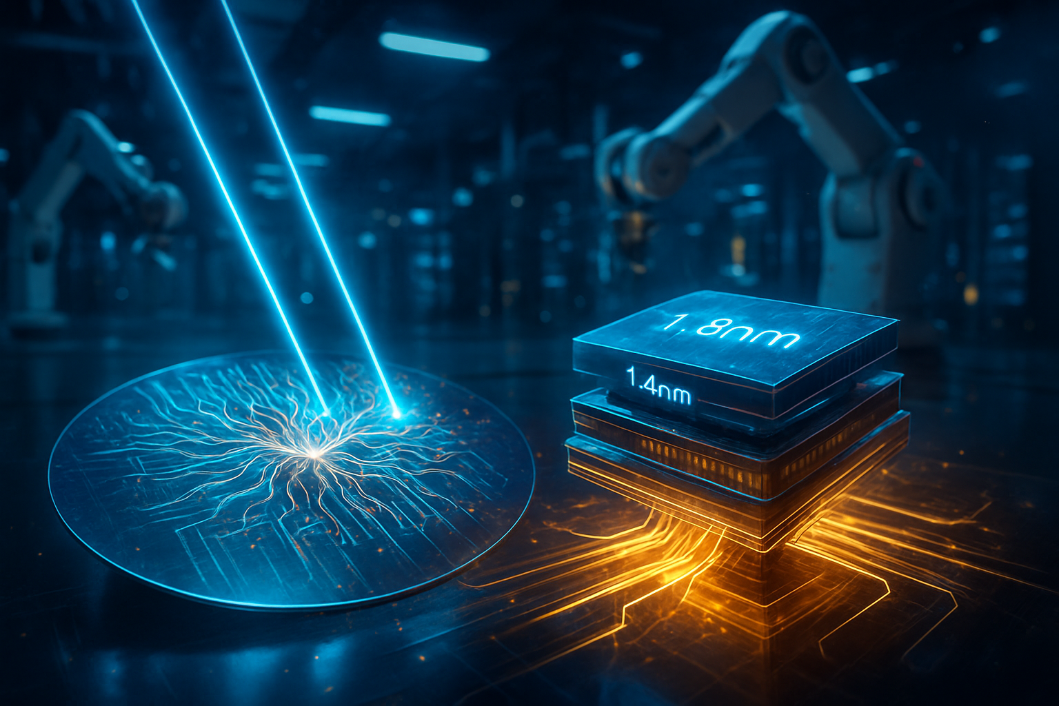
Looking ahead, the roadmap for 2027 and beyond is already taking shape. The industry is preparing for the transition to 1.4nm (A14) nodes, which will rely heavily on High-NA (Numerical Aperture) EUV lithography. Intel (NASDAQ: INTC) has taken an early lead in adopting these $380 million machines from ASML (NASDAQ: ASML), aiming to use them for its 14A node by late 2026. High-NA EUV allows for even finer resolution, enabling the printing of features that are nearly half the size of current limits, though the "stitching" of smaller exposure fields remains a significant technical challenge for high-volume yields.
Beyond the 1.4nm node, the industry is already eyeing the successor to the Nanosheet: the Complementary FET (CFET). While Nanosheets stack multiple layers of the same type of transistor, CFETs will stack n-type and p-type transistors directly on top of each other. This vertical integration could theoretically double the transistor density once again, potentially pushing the industry toward the 1nm (A10) threshold by the end of the decade. Research at institutions like imec suggests that CFET will be the standard by 2030, though the thermal management of such densely packed structures remains a major hurdle.
The near-term challenge for the industry will be yield optimization. As of early 2026, 2nm yields are estimated to be in the 60-70% range for TSMC and slightly lower for Intel. Improving these numbers is critical for making 2nm chips accessible to a wider range of applications, including consumer-grade edge AI devices and automotive systems. Experts predict that as yields stabilize throughout 2026, we will see a surge in "On-Device AI" capabilities, where complex LLMs can run locally on smartphones and laptops without sacrificing battery life.
A New Chapter in Computing History
The transition to Nanosheet GAA transistors marks the beginning of a new chapter in the history of computing. By successfully re-engineering the transistor for the 2nm era, TSMC, Intel, and Samsung have provided the physical foundation upon which the next decade of AI innovation will be built. The move from FinFET to GAA is not merely a technical upgrade; it is a necessary evolution that allows the digital world to continue expanding in the face of daunting physical and environmental constraints.
As we move through 2026, the key takeaways are clear: the "Power Wall" has been temporarily breached, the competitive landscape has been narrowed to a handful of "Silicon Elite" players, and the geopolitical importance of the semiconductor supply chain has never been higher. The successful mass production of 2nm GAA chips ensures that the AI revolution will have the hardware it needs to reach its full potential.
In the coming months, the industry will be watching for the first consumer benchmarks of 2nm-powered devices and the progress of Intel’s 18A external foundry partnerships. While the road to 1nm remains fraught with technical and economic challenges, the Nanosheet revolution has proven that the semiconductor industry is still capable of reinventing itself at the atomic level to power the future of intelligence.
This content is intended for informational purposes only and represents analysis of current AI developments.
TokenRing AI delivers enterprise-grade solutions for multi-agent AI workflow orchestration, AI-powered development tools, and seamless remote collaboration platforms.
For more information, visit https://www.tokenring.ai/.