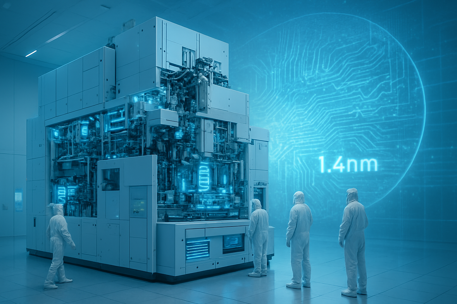
The semiconductor industry has officially entered a new epoch. As of January 1, 2026, the transition from traditional transistor layouts to the "Angstrom Era" is no longer a roadmap projection but a physical reality. At the heart of this shift is Intel Corporation (Nasdaq: INTC) and its 18A process node, which has successfully integrated Backside Power Delivery (branded as PowerVia) into high-volume manufacturing. This architectural pivot represents the most significant change to chip design since the introduction of FinFET transistors over a decade ago, fundamentally altering how electricity reaches the billions of switches that power modern artificial intelligence.
The immediate significance of this breakthrough cannot be overstated. By decoupling the power delivery network from the signal routing layers, Intel has effectively solved the "routing congestion" crisis that has plagued chip designers for years. As AI models grow exponentially in complexity, the hardware required to run them—GPUs, NPUs, and specialized accelerators—demands unprecedented current densities and signal speeds. The successful deployment of 18A provides a critical performance-per-watt advantage that is already reshaping the competitive landscape for data center infrastructure and edge AI devices.
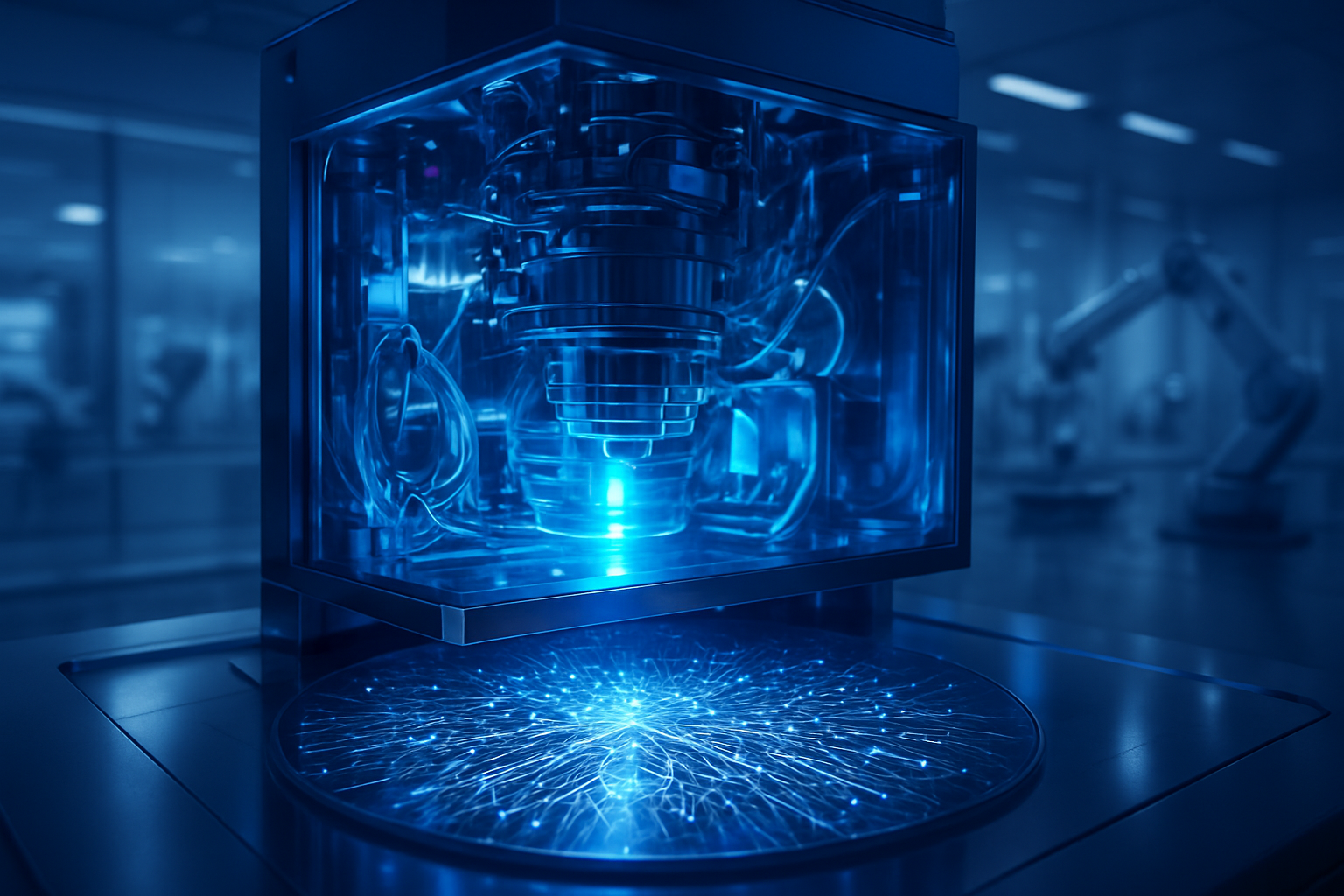
The Technical Architecture of PowerVia: Flipping the Script on Silicon
For decades, microchips were built like a house where the plumbing and electrical wiring were all crammed into the same narrow crawlspace as the data cables. In traditional "front-side" power delivery, both power and signal wires are layered on top of the transistors. As transistors shrunk, these wires became so densely packed that they interfered with one another, leading to electrical resistance and "IR drop"—a phenomenon where voltage decreases as it travels through the chip. Intel’s PowerVia solves this by moving the entire power distribution network to the back of the silicon wafer. Using "Nano-TSVs" (Through-Silicon Vias), power is delivered vertically from the bottom, while the front-side metal layers are dedicated exclusively to signal routing.
This separation provides a dual benefit: it eliminates the "spaghetti" of wires that causes signal interference and allows for significantly thicker, less resistive power rails on the backside. Technical specifications from the 18A node indicate a 30% reduction in IR drop, ensuring that transistors receive a stable, consistent voltage even under the massive computational loads required for Large Language Model (LLM) training. Furthermore, because the front side is no longer cluttered with power lines, Intel has achieved a cell utilization rate of over 90%, allowing for a logic density improvement of approximately 30% compared to previous generation nodes like Intel 3.
Initial reactions from the semiconductor research community have been overwhelmingly positive, with experts noting that Intel has successfully executed a "once-in-a-generation" manufacturing feat. While rivals like Taiwan Semiconductor Manufacturing Co. (NYSE: TSM) and Samsung Electronics (OTC: SSNLF) are working on their own versions of backside power—TSMC’s "Super PowerRail" on its A16 node—Intel’s early lead in high-volume manufacturing gives it a rare technical "sovereignty" in the sub-2nm space. The 18A node’s ability to deliver a 6% frequency gain at iso-power, or up to a 40% reduction in power consumption at lower voltages, sets a new benchmark for the industry.
Strategic Shifts: Intel’s Foundry Resurgence and the AI Arms Race
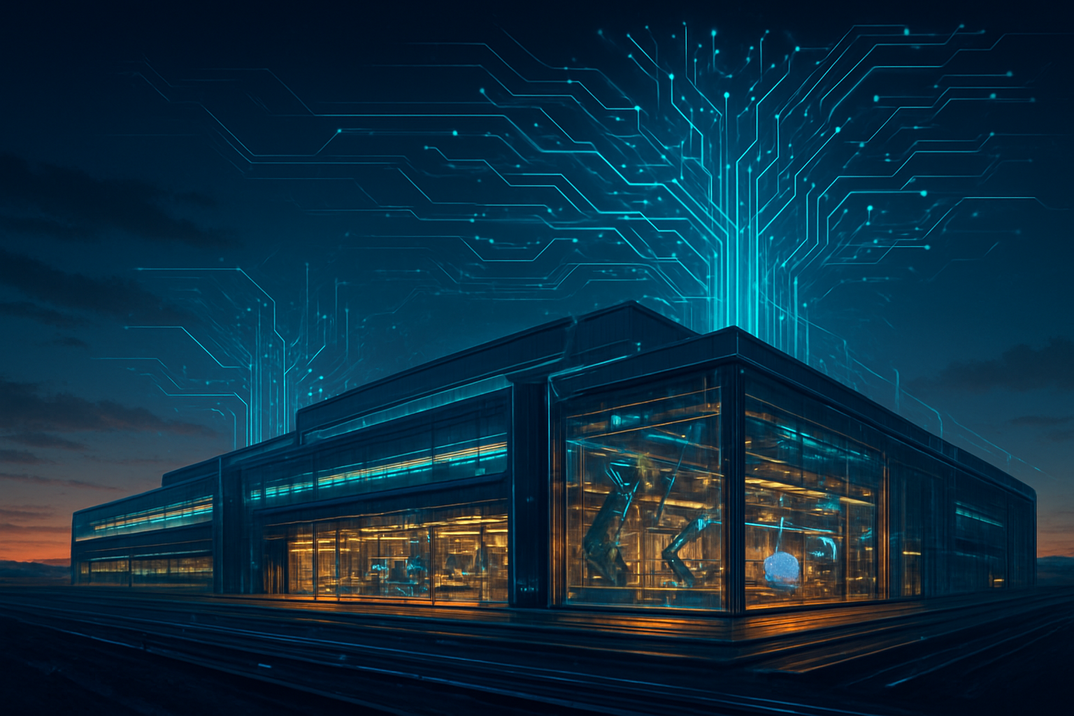
The successful ramp of 18A at Fab 52 in Arizona has profound implications for the global foundry market. For years, Intel struggled to catch up to TSMC’s manufacturing lead, but PowerVia has provided the company with a unique selling proposition for its Intel Foundry services. Major tech giants are already voting with their capital; Microsoft (Nasdaq: MSFT) has confirmed that its next-generation Maia 3 (Griffin) AI accelerators are being built on the 18A node to take advantage of its efficiency gains. Similarly, Amazon (Nasdaq: AMZN) and NVIDIA (Nasdaq: NVDA) are reportedly sampling 18A-P (Performance) silicon for future data center products.
This development disrupts the existing hierarchy of the AI chip market. By being the first to market with backside power, Intel is positioning itself as the primary alternative to TSMC for high-end AI silicon. For startups and smaller AI labs, the increased efficiency of 18A-based chips means lower operational costs for inference and training. The strategic advantage here is clear: companies that can migrate their designs to 18A early will benefit from higher clock speeds and lower thermal envelopes, potentially allowing for more compact and powerful AI hardware in both the data center and consumer "AI PCs."
Scaling Moore’s Law in the Era of Generative AI
Beyond the immediate corporate rivalries, the arrival of PowerVia and the 18A node represents a critical milestone in the broader AI landscape. We are currently in a period where the demand for compute is outstripping the historical gains of Moore’s Law. Backside power delivery is one of the "miracle" technologies required to keep the industry on its scaling trajectory. By solving the power delivery bottleneck, 18A allows for the creation of chips that can handle the massive "burst" currents required by generative AI models without overheating or suffering from signal degradation.
However, this advancement does not come without concerns. The complexity of manufacturing backside power networks is immense, requiring precision wafer bonding and thinning processes that are prone to yield issues. While Intel has reported yields in the 60-70% range for early 18A production, maintaining these levels as they scale to millions of units will be a significant challenge. Comparisons are already being made to the industry's transition from planar to FinFET transistors in 2011; just as FinFET enabled the mobile revolution, PowerVia is expected to be the foundational technology for the "AI Everywhere" era.
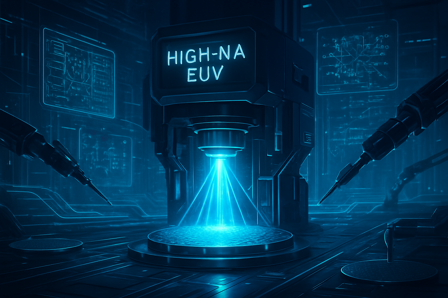
The Road to 14A and the Future of 3D Integration
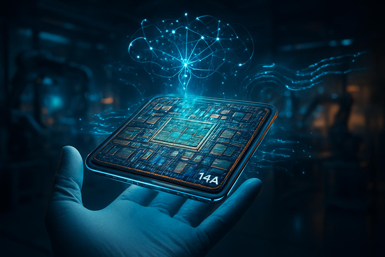
Looking ahead, the 18A node is just the beginning of a broader roadmap toward 3D silicon integration. Intel has already teased its 14A node, which is expected to further refine PowerVia technology and introduce High-NA EUV (Extreme Ultraviolet) lithography at scale. Near-term developments will likely focus on "complementary FETs" (CFETs), where n-type and p-type transistors are stacked on top of each other, further increasing density. When combined with backside power, CFETs could lead to a 50% reduction in chip area, allowing for even more powerful AI cores in the same physical footprint.
The long-term potential for these technologies extends into the realm of "system-on-wafer" designs, where entire wafers are treated as a single, interconnected compute fabric. The primary challenge moving forward will be thermal management; as chips become denser and power is delivered from the back, traditional cooling methods may reach their limits. Experts predict that the next five years will see a surge in liquid-to-chip cooling solutions and new thermal interface materials designed specifically for backside-powered architectures.
A Decisive Moment for Silicon Sovereignty
In summary, the launch of Intel 18A with PowerVia marks a decisive victory for Intel’s turnaround strategy and a pivotal moment for the technology industry. By being the first to successfully implement backside power delivery in high-volume manufacturing, Intel has reclaimed a seat at the leading edge of semiconductor physics. The key takeaways are clear: 18A offers a substantial leap in efficiency and performance, it has already secured major AI customers like Microsoft, and it sets the stage for the next decade of silicon scaling.
This development is significant not just for its technical metrics, but for its role in sustaining the AI revolution. As we move further into 2026, the industry will be watching closely to see how TSMC responds with its A16 node and how quickly Intel can scale its Arizona and Ohio fabs to meet the insatiable demand for AI compute. For now, the "Angstrom Era" is here, and it is being powered from the back.
This content is intended for informational purposes only and represents analysis of current AI developments.
TokenRing AI delivers enterprise-grade solutions for multi-agent AI workflow orchestration, AI-powered development tools, and seamless remote collaboration platforms.
For more information, visit https://www.tokenring.ai/.