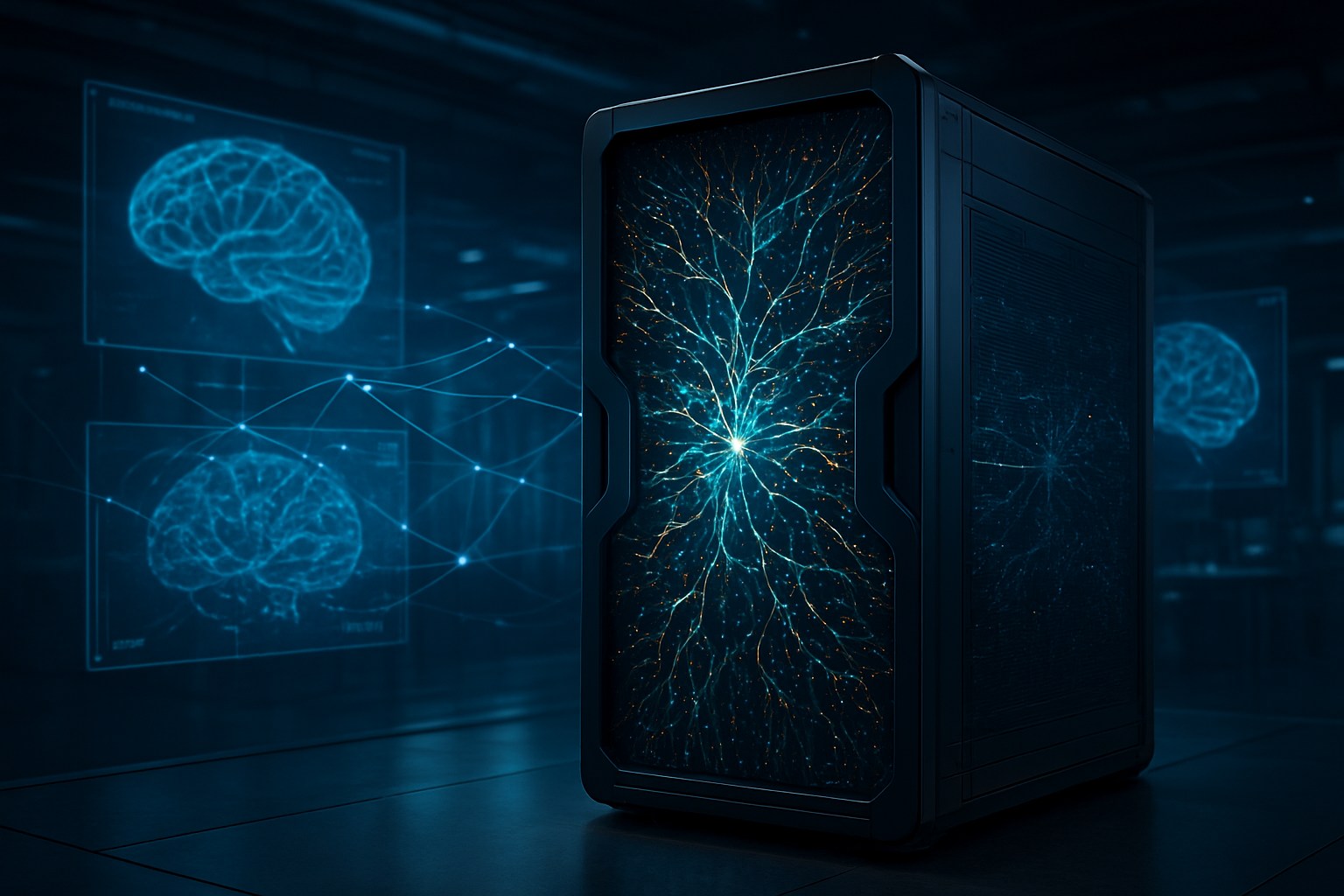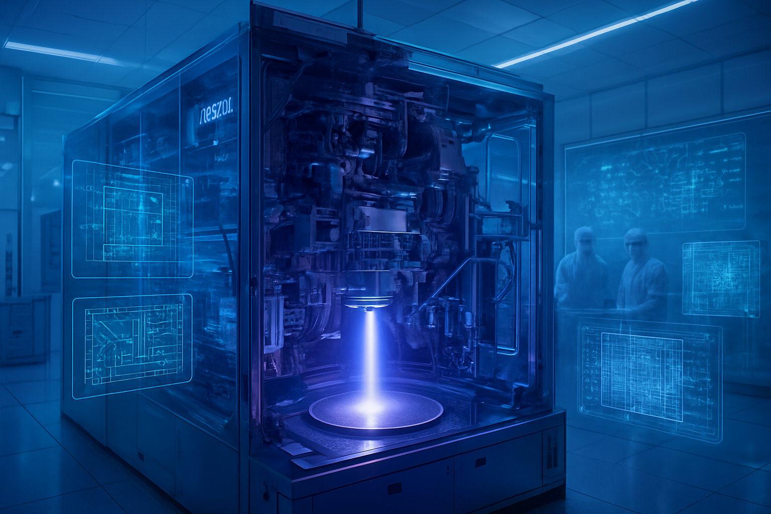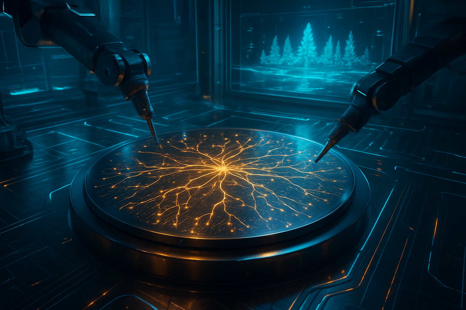
The semiconductor industry has reached a definitive turning point as of February 2026, marking the most significant architectural shift in transistor design since the move to FinFET a decade ago. Backside Power Delivery Network (BSPDN) technology has officially moved from laboratory prototypes to high-volume manufacturing (HVM), effectively "flipping the wafer" to solve the critical power and routing bottlenecks that threatened to stall the progress of next-generation artificial intelligence accelerators.
This breakthrough arrives at a critical juncture for the AI industry. As generative AI models continue to scale, requiring chips with power envelopes exceeding 1,000 watts, the traditional method of delivering electricity through the top of the silicon die had become a liability. By separating the "data" wires from the "power" wires, foundries are now delivering chips that run faster, cooler, and with significantly higher efficiency, providing the necessary hardware foundation for the next leap in AI compute capability.
The Architecture of the Angstrom Era: PowerVia vs. Super Power Rail
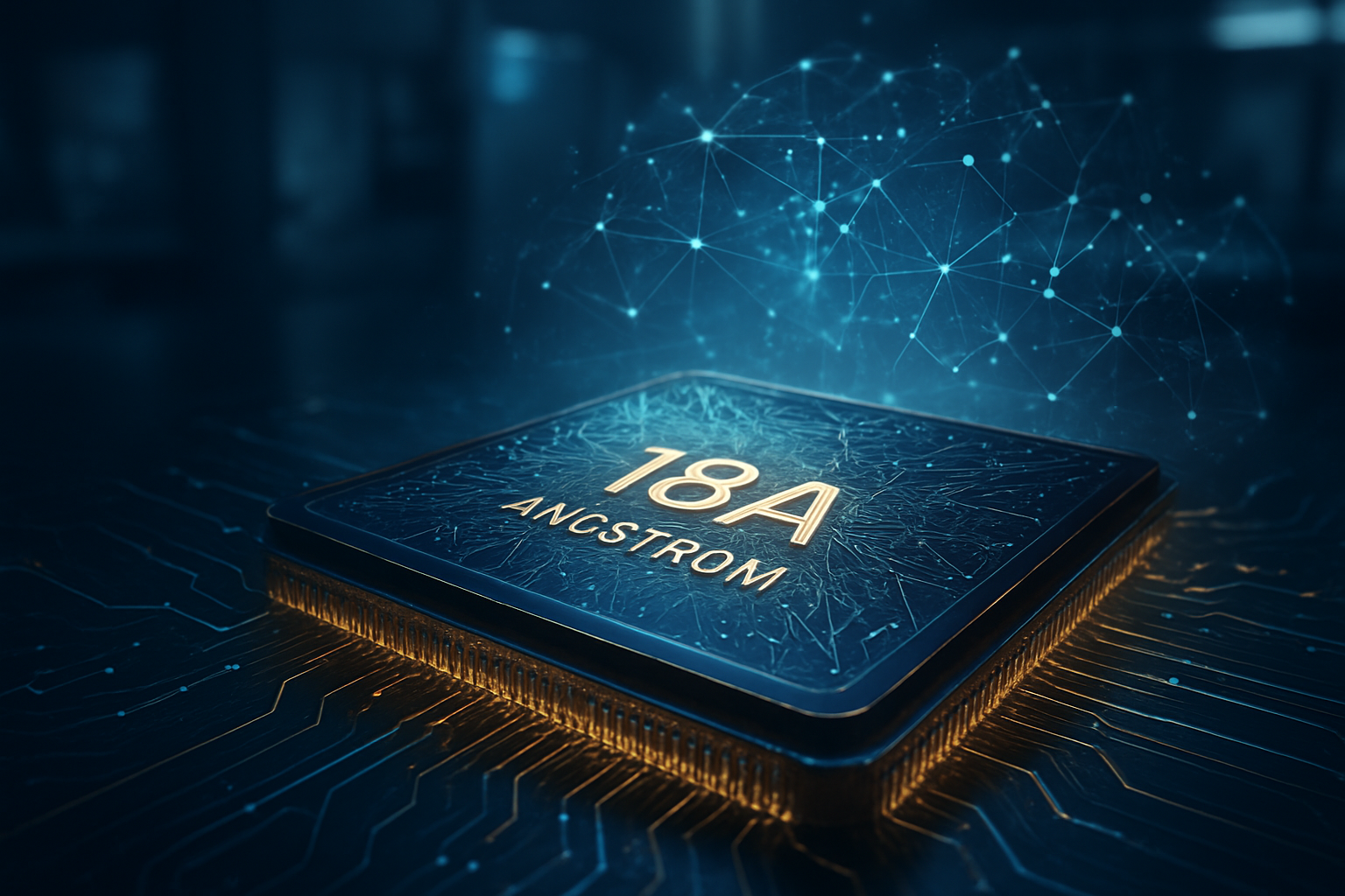
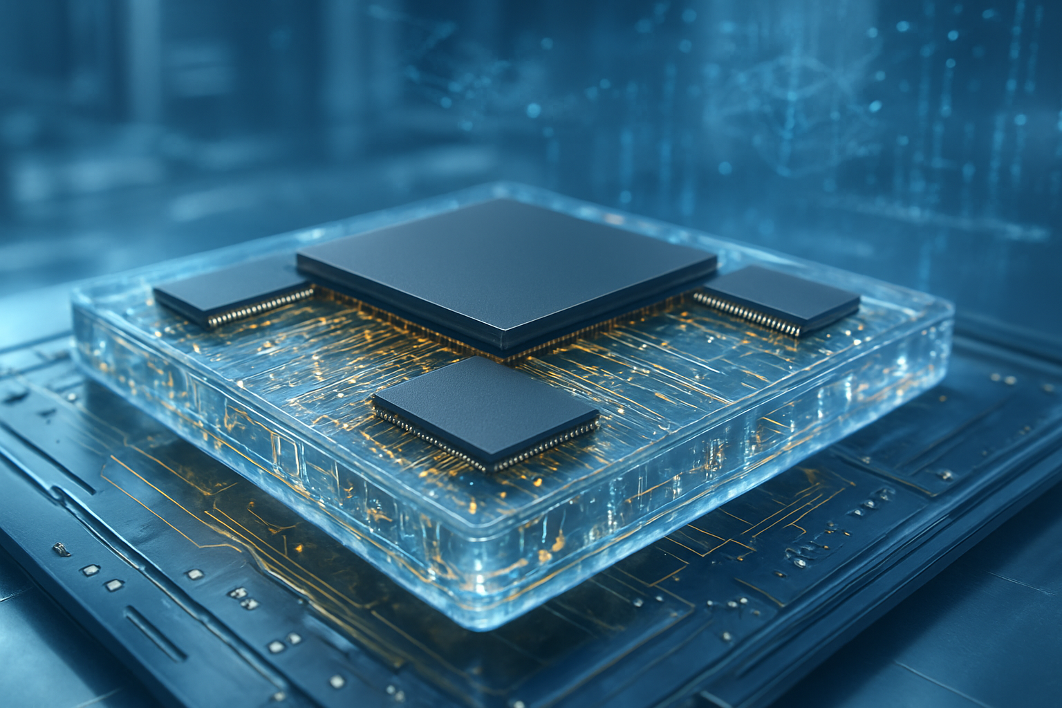
At the heart of this revolution is a technical rivalry between the world’s leading foundries. Intel (NASDAQ: INTC) has achieved a major strategic victory by hitting high-volume manufacturing first with its PowerVia technology on the Intel 18A node. In January 2026, Intel’s Fab 52 in Arizona began shipping the first "Clearwater Forest" server processors to data center customers, proving that its unique "Nano-TSV" (Through Silicon Via) approach could be scaled reliably. Intel’s implementation uses tiny vertical connections to link the backside power network to the metal layers just above the transistors, a method that has demonstrated a remarkable 69% reduction in static IR drop (voltage droop).
In contrast, TSMC (NYSE: TSM) is preparing to launch its Super Power Rail architecture with the A16 node, scheduled for HVM in the second half of 2026. While TSMC is arriving slightly later to the market, its implementation is technically more ambitious. Instead of using Nano-TSVs to connect to intermediate metal layers, TSMC’s Super Power Rail connects the backside power network directly to the transistor’s source and drain. This "direct contact" method is more difficult to manufacture but promises even greater efficiency gains, with TSMC projecting an 8–10% speed improvement and a 15–20% power reduction compared to its previous 2nm (N2) node.
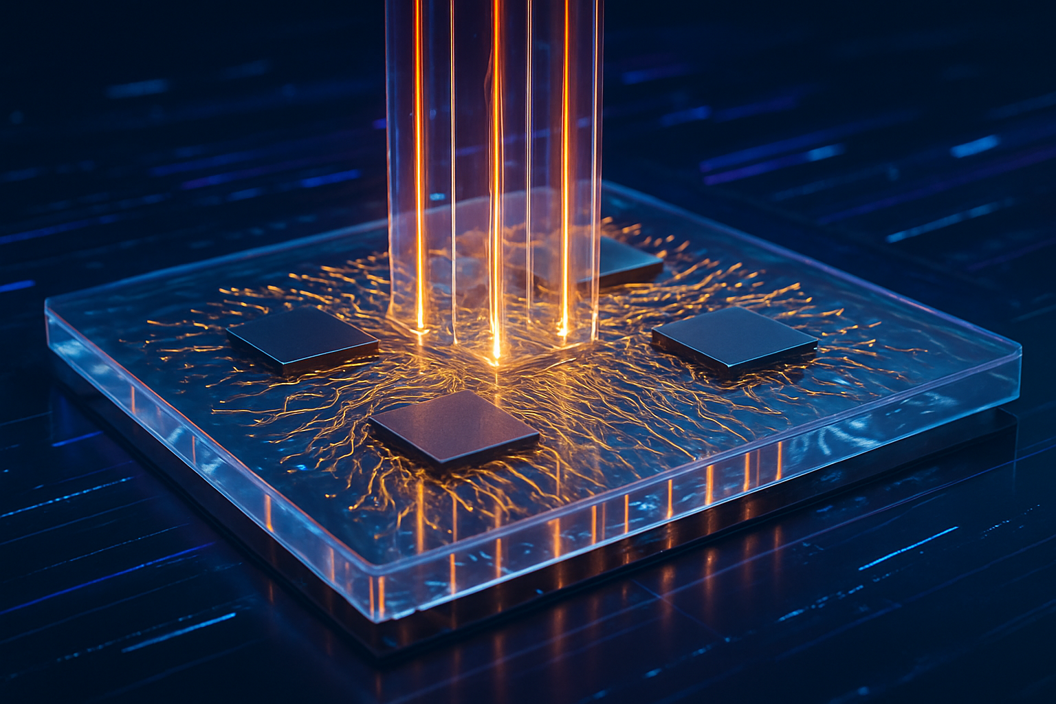
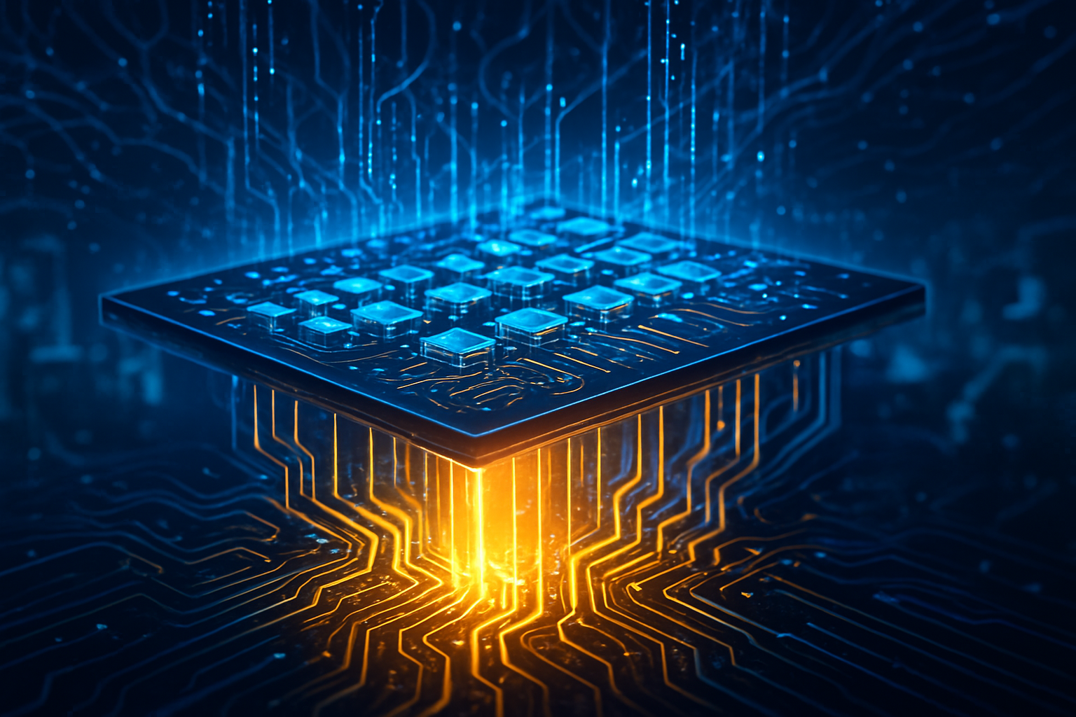
The primary advantage of both approaches is the near-total elimination of routing congestion. In traditional chips, power and signal wires are tangled together in a "spaghetti" of up to 20 layers of metal on top of the transistors. Moving power to the backside frees up roughly 20% of the front-side routing resources, allowing signal wires to be wider and more direct. This relief has enabled chip designers to achieve a voltage droop of less than 1%, ensuring that AI processors can maintain peak clock frequencies without the instability that previously plagued high-performance silicon.
Strategic Realignment: NVIDIA and the Hyperscale Shuffle
The arrival of BSPDN has fundamentally altered the competitive landscape for AI chip giants. NVIDIA (NASDAQ: NVDA), which previously relied almost exclusively on TSMC for its high-end GPUs, has made a historic pivot toward a multi-foundry strategy. In late 2025, NVIDIA reportedly took a $5 billion stake in Intel Foundry to secure capacity for domestic manufacturing. While NVIDIA's core compute dies for its 2026 "Feynman" architecture remain with TSMC's A16 node, the company is utilizing Intel’s 18A process for its I/O dies and advanced packaging. This move allows NVIDIA to bypass the persistent capacity bottlenecks at TSMC while leveraging Intel's early lead in backside power.
Samsung (KRX: 005930) has also emerged as a formidable player in this era, achieving 70% yields on its SF2P process as of early 2026. By utilizing its third-generation Gate-All-Around (GAA) experience, Samsung has become a "release valve" for companies like Advanced Micro Devices (NASDAQ: AMD) and Broadcom (NASDAQ: AVGO). AMD is reportedly dual-sourcing its "EPYC Venice" server chips between TSMC and Samsung to ensure supply stability for the massive AI build-outs being undertaken by hyperscalers.
For the "Big Three" cloud providers—Microsoft (NASDAQ: MSFT), Alphabet (NASDAQ: GOOGL), and Meta (NASDAQ: META)—the efficiency gains of BSPDN are a financial necessity. With annual AI capital expenditures reaching hundreds of billions of dollars, the 15–25% energy savings offered by these new nodes translate directly into lower Total Cost of Ownership (TCO). These savings allow hyperscalers to pack more 1,000W+ chips into existing data centers without requiring immediate, expensive upgrades to liquid cooling infrastructure.
Breaking the Power Wall: A Milestone for Moore’s Law
The broader significance of Backside Power Delivery cannot be overstated; it is the technology that effectively "saved" the scaling roadmap for the late 2020s. For years, the semiconductor industry faced a "Power Wall," where the resistance of increasingly thin power wires caused so much heat and voltage loss that further transistor shrinking yielded diminishing returns. BSPDN has broken this wall by providing a dedicated, low-resistance highway for electricity, allowing Moore's Law to continue into the "Angstrom Era."
This milestone is comparable to the introduction of High-K Metal Gate (HKMG) in 2007 or the transition to EUV (Extreme Ultraviolet) lithography in 2019. It marks a shift from 2D planar thinking to a truly 3D approach to chip architecture. However, this transition is not without its risks. The process of thinning a silicon wafer to just a few hundred nanometers to enable backside connections is incredibly delicate. Initial reports suggest that Intel's yields on 18A are currently in the 55–65% range, which is a significant hurdle to long-term profitability compared to the 70%+ yields typically expected of mature nodes.
Furthermore, the environmental impact of this shift is double-edged. While the chips themselves are more efficient, the manufacturing process for BSPDN nodes requires more complex lithography and bonding steps, increasing the carbon footprint of the fabrication process. Industry experts are closely watching how foundries balance the demand for high-performance AI silicon with increasingly stringent ESG (Environmental, Social, and Governance) requirements.
Beyond 2026: CFETs and the $400 Million Machines
Looking toward the 2027–2030 horizon, the foundation laid by BSPDN will enable even more exotic architectures. The next major step is the Complementary FET (CFET), which stacks n-type and p-type transistors vertically on top of each other. Researchers predict that combining CFET with BSPDN could reduce chip area by another 40–50%, potentially leading to 1nm and sub-1nm nodes by the end of the decade.
The industry is also racing to integrate Silicon Photonics directly onto the backside of the wafer. By 2028, we expect to see the first "Optical BSPDN" designs, where data is moved across the chip using light instead of electricity. This would solve the "Interconnect Bottleneck," allowing for Terabit-per-second communication between different parts of an AI processor with near-zero heat generation.
However, the cost of this progress is staggering. The move to the 1.4nm (A14) and 10A nodes will require ASML’s (NASDAQ: ASML) High-NA EUV tools, which now cost upwards of $400 million per machine. This extreme capital intensity is likely to further consolidate the market, leaving only Intel, TSMC, and Samsung capable of competing at the bleeding edge, while smaller foundries focus on legacy and specialty nodes.
A New Foundation for Artificial Intelligence
The successful rollout of Backside Power Delivery in early 2026 marks the beginning of the "Angstrom Era" in earnest. Intel’s PowerVia has proven that the "power flip" is commercially viable, while TSMC’s upcoming Super Power Rail promises to push the boundaries of efficiency even further. This technology has arrived just in time to sustain the explosive growth of generative AI, providing the thermal and electrical headroom required for the next generation of massive neural networks.
The key takeaway for the coming months will be the "Yield Race." While the technical benefits of BSPDN are clear, the foundry that can produce these complex chips with the highest reliability will ultimately capture the lion's share of the AI market. As Intel ramps up its 18A production and TSMC moves into risk production for A16, the semiconductor industry has never been more vital to the global economy—or more technically challenging.
This content is intended for informational purposes only and represents analysis of current AI and semiconductor developments as of February 2026.
TokenRing AI delivers enterprise-grade solutions for multi-agent AI workflow orchestration, AI-powered development tools, and seamless remote collaboration platforms.
For more information, visit https://www.tokenring.ai/.