Tag: Intel

  • The Silicon Sovereign: How 2026 Became the Year the AI PC Reclaimed the Edge

    The Silicon Sovereign: How 2026 Became the Year the AI PC Reclaimed the Edge

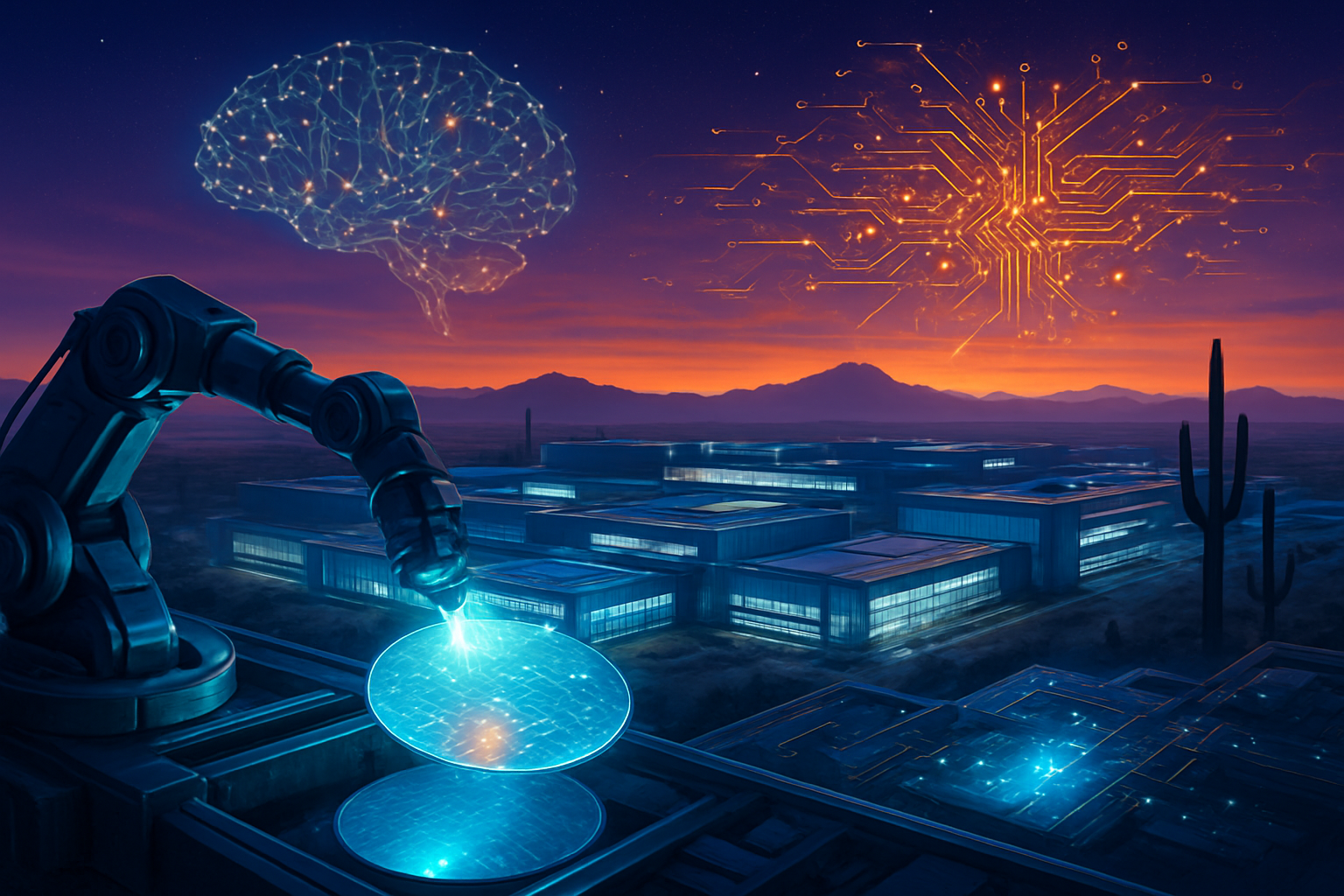
    As we close out 2025 and head into 2026, the personal computer is undergoing its most radical transformation since the introduction of the graphical user interface. The "AI PC" has moved from a marketing buzzword to the definitive standard for modern computing, driven by a fierce arms race between silicon giants to pack unprecedented neural processing power into laptops and desktops. By the start of 2026, the industry has crossed a critical threshold: the ability to run sophisticated Large Language Models (LLMs) entirely on local hardware, fundamentally shifting the gravity of artificial intelligence from the cloud back to the edge.

    This transition is not merely about speed; it represents a paradigm shift in digital sovereignty. With the latest generation of processors from Qualcomm (NASDAQ: QCOM), Intel (NASDAQ: INTC), and AMD (NASDAQ: AMD) now exceeding 45–50 Trillion Operations Per Second (TOPS) on the Neural Processing Unit (NPU) alone, the "loading spinner" of cloud-based AI is becoming a relic of the past. For the first time, users are experiencing "instant-on" intelligence that doesn't require an internet connection, doesn't sacrifice privacy, and doesn't incur the subscription fatigue of the early 2020s.

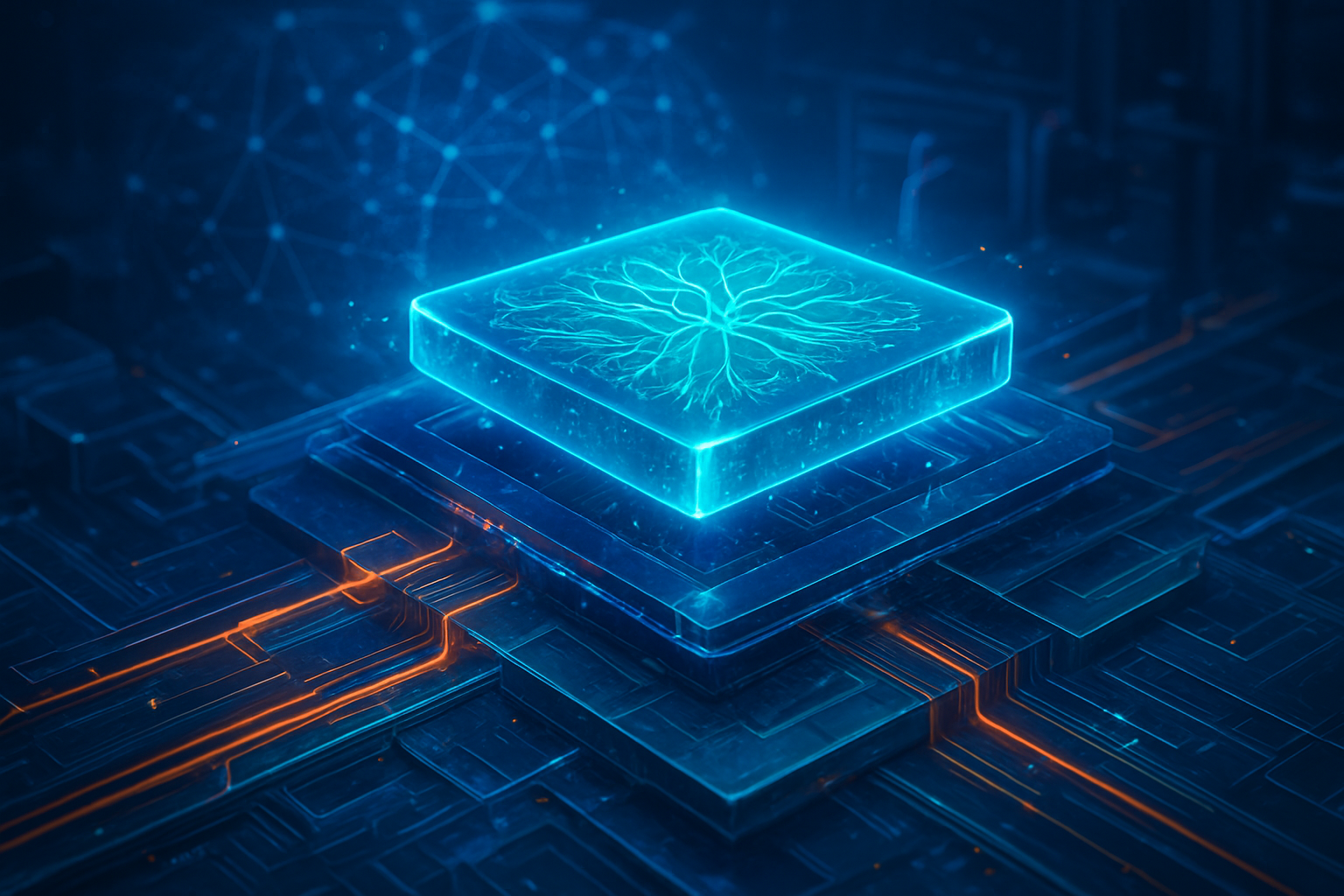
    The 50-TOPS Threshold: Inside the Silicon Arms Race

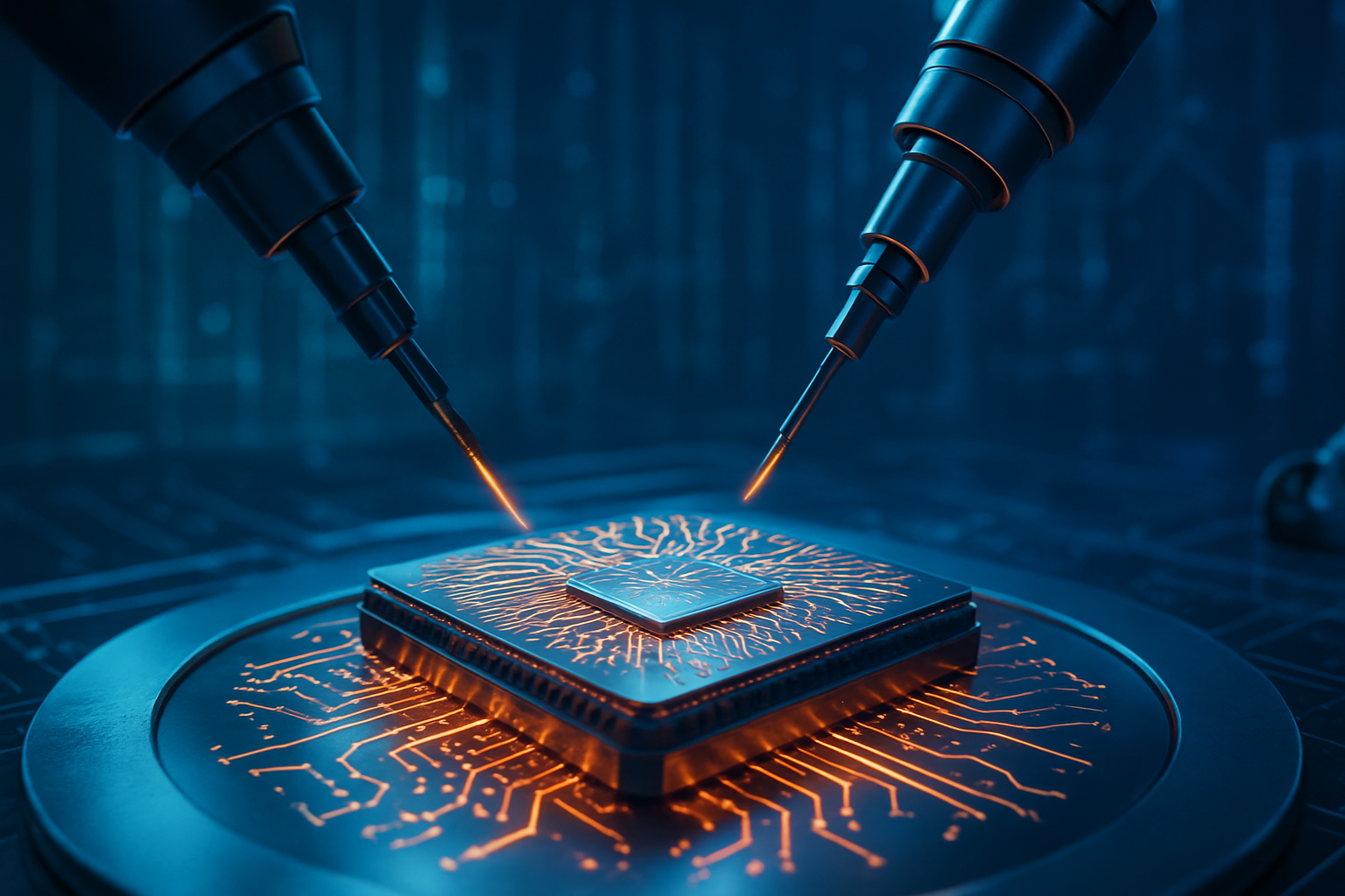
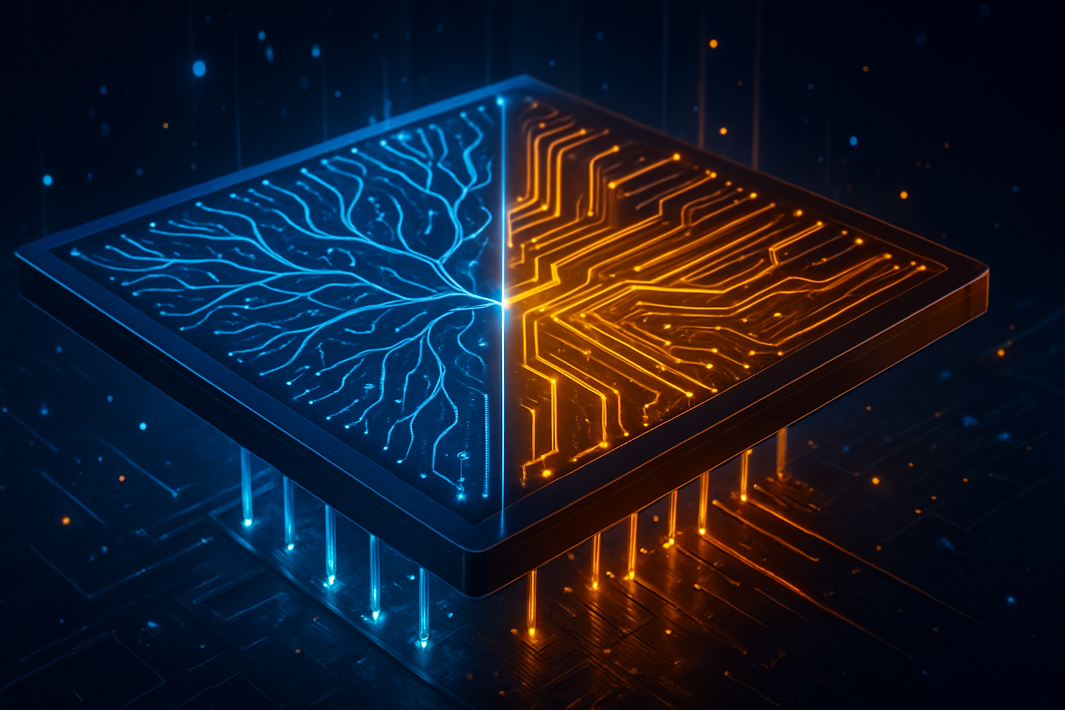
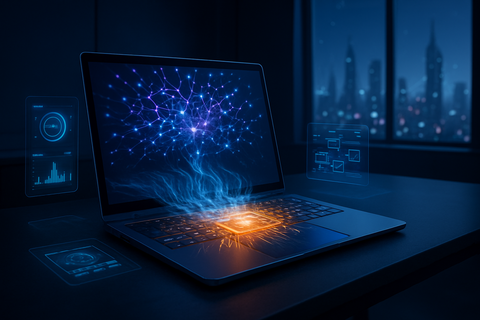
    The technical heart of the 2026 AI PC revolution lies in the NPU, a specialized accelerator designed specifically for the matrix mathematics that power AI. Leading the charge is Qualcomm (NASDAQ: QCOM) with its second-generation Snapdragon X2 Elite. Confirmed for a broad rollout in the first half of 2026, the Snapdragon X2’s Hexagon NPU has jumped to a staggering 80 TOPS. This allows the chip to run 3-billion parameter models, such as Microsoft’s Phi-3 or Meta’s Llama 3.2, at speeds exceeding 200 tokens per second—faster than a human can read.

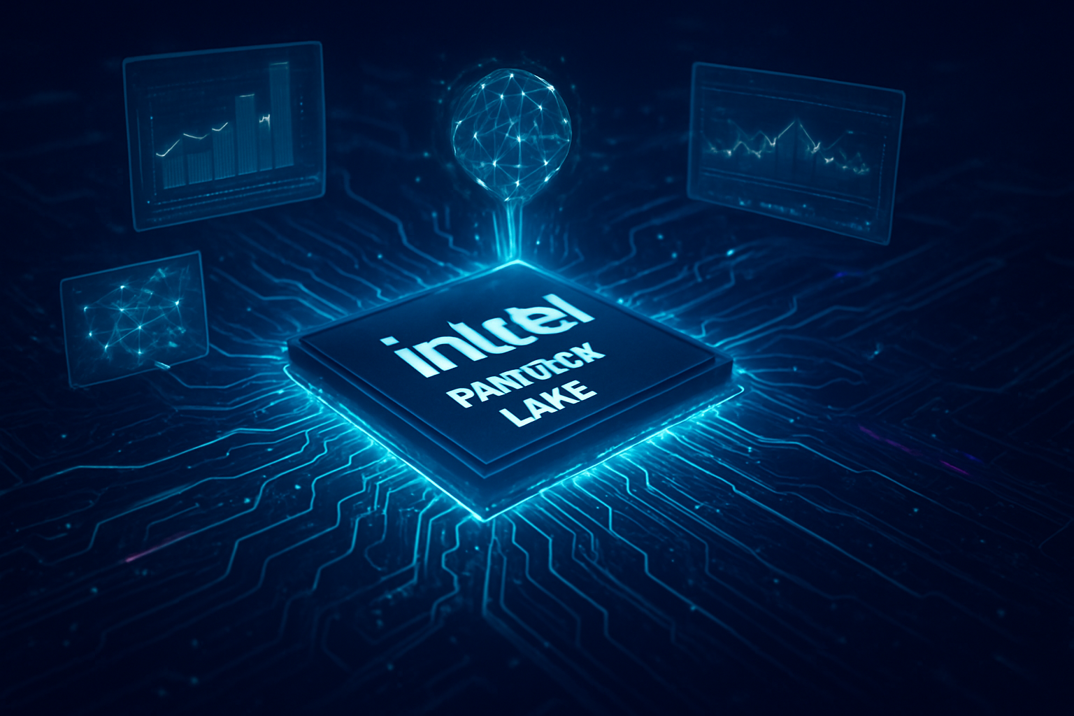
    Intel (NASDAQ: INTC) has responded with its Panther Lake architecture (Core Ultra Series 3), built on the cutting-edge Intel 18A process node. Panther Lake’s NPU 5 delivers a dedicated 50 TOPS, but Intel’s "Total Platform" approach pushes the combined AI performance of the CPU, GPU, and NPU to over 180 TOPS. Meanwhile, AMD (NASDAQ: AMD) has solidified its position with the Strix Point and Krackan platforms. AMD’s XDNA 2 architecture provides a consistent 50 TOPS across its Ryzen AI 300 series, ensuring that even mid-range laptops priced under $999 can meet the stringent requirements for "Copilot+" certification.

    This hardware leap differs from previous generations because it prioritizes "Agentic AI." Unlike the basic background blur or noise cancellation of 2024, the 2026 hardware is optimized for 4-bit and 8-bit quantization. This allows the NPU to maintain "always-on" background agents that can index every document, email, and meeting on a device in real-time without draining the battery. Industry experts note that this local-first approach reduces the latency of AI interactions from seconds to milliseconds, making the AI feel like a seamless extension of the operating system rather than a remote service.

    Disrupting the Cloud: The Business of Local Intelligence

    The rise of the AI PC is sending shockwaves through the business models of tech giants. Microsoft (NASDAQ: MSFT) has been the primary architect of this shift, pivoting its Windows AI Foundry to allow developers to build models that "scale down" to local NPUs. This reduces Microsoft’s massive server costs for Azure while giving users a more responsive experience. However, the most significant disruption is felt by NVIDIA (NASDAQ: NVDA). While NVIDIA remains the king of the data center, the high-performance NPUs from Intel and AMD are beginning to cannibalize the market for entry-level discrete GPUs (dGPUs). Why buy a dedicated graphics card for AI when your integrated NPU can handle 4K upscaling and local LLM chat more efficiently?

    The competitive landscape is further complicated by Apple (NASDAQ: AAPL), which has integrated "Apple Intelligence" across its entire M-series Mac lineup. By 2026, the battle for "Silicon Sovereignty" has forced cloud-first companies like Alphabet (NASDAQ: GOOGL) and Amazon (NASDAQ: AMZN) to adapt. Google has optimized its Gemini Nano model specifically for these new NPUs, ensuring that Chrome remains the dominant gateway to AI, whether that AI is running in the cloud or on the user's desk.

    For startups, the AI PC era has birthed a new category of "AI-Native" software. Tools like Cursor and Bolt are moving beyond simple code completion to "Vibe Engineering," where local agents execute complex software architectures entirely on-device. This has created a massive strategic advantage for companies that can provide high-performance local execution, as enterprises increasingly demand "air-gapped" AI to protect their proprietary data from leaking into public training sets.

    Privacy, Latency, and the Death of the Loading Spinner

    Beyond the corporate maneuvering, the wider significance of the AI PC lies in its impact on privacy and user experience. For the past decade, the tech industry has moved toward a "thin client" model where the most powerful features lived on someone else's server. The AI PC reverses this trend. By processing data locally, users regain "data residency"—the assurance that their most personal thoughts, financial records, and private photos never leave their device. This is a significant milestone in the broader AI landscape, addressing the primary concern that has held back enterprise adoption of generative AI.

    Latency is the other silent revolution. In the cloud-AI era, every query was subject to network congestion and server availability. In 2026, the "death of the loading spinner" has changed how humans interact with computers. When an AI can respond instantly to a voice command or a gesture, it stops being a "tool" and starts being a "collaborator." This is particularly impactful for accessibility; tools like Cephable now use local NPUs to translate facial expressions into complex computer commands with zero lag, providing a level of autonomy previously impossible for users with motor impairments.

    However, this shift is not without concerns. The "Recall" features and always-on indexing that NPUs enable have raised significant surveillance questions. While the data stays local, the potential for a "local panopticon" exists if the operating system itself is compromised. Comparisons are being drawn to the early days of the internet: we are gaining incredible new capabilities, but we are also creating a more complex security perimeter that must be defended at the silicon level.

    The Road to 2027: Agentic Workflows and Beyond

    Looking ahead, the next 12 to 24 months will see the transition from "Chat AI" to "Agentic Workflows." In this near-term future, your PC won't just help you write an email; it will proactively manage your calendar, negotiate with other agents to book travel, and automatically generate reports based on your work habits. Intel’s upcoming Nova Lake and AMD’s Zen 6 "Medusa" architecture are already rumored to target 75–100+ TOPS, which will be necessary to run the "thinking" models that power these autonomous agents.

    One of the most anticipated developments is NVIDIA’s rumored entry into the PC CPU market. Reports suggest NVIDIA is co-developing an ARM-based processor with MediaTek, designed to bring Blackwell-level AI performance to the "Thin & Light" laptop segment. This would represent a direct challenge to Qualcomm’s dominance in the ARM-on-Windows space and could spark a new era of "AI Workstations" that blur the line between a laptop and a server.

    The primary challenge remains software optimization. While the hardware is ready, many legacy applications have yet to be rewritten to take advantage of the NPU. Experts predict that 2026 will be the year of the "AI Refactor," as developers race to move their most compute-intensive features off the CPU/GPU and onto the NPU to save battery life and improve performance.

    A New Era of Personal Computing

    The rise of the AI PC in 2026 marks the end of the "General Purpose" computing era and the beginning of the "Contextual" era. We have moved from computers that wait for instructions to computers that understand intent. The convergence of 50+ TOPS NPUs, efficient Small Language Models, and a robust local-first software ecosystem has fundamentally altered the trajectory of the tech industry.

    The key takeaway for 2026 is that the cloud is no longer the only place where "magic" happens. By reclaiming the edge, the AI PC has made artificial intelligence faster, more private, and more personal. In the coming months, watch for the launch of the first truly autonomous "Agentic" OS updates and the arrival of NVIDIA’s ARM-based silicon, which could redefine the performance ceiling for the entire industry. The PC isn't just back; it's smarter than ever.


    This content is intended for informational purposes only and represents analysis of current AI developments.

    TokenRing AI delivers enterprise-grade solutions for multi-agent AI workflow orchestration, AI-powered development tools, and seamless remote collaboration platforms.
    For more information, visit https://www.tokenring.ai/.

  • The Sub-2nm Supremacy: Intel 18A Hits Volume Production as TSMC N2 Ramps for 2026

    The Sub-2nm Supremacy: Intel 18A Hits Volume Production as TSMC N2 Ramps for 2026

    As of late December 2025, the semiconductor industry has reached a historic inflection point that many analysts once thought impossible. Intel (NASDAQ:INTC) has officially successfully executed its "five nodes in four years" roadmap, culminating in the mid-2025 volume production of its 18A (1.8nm) process node. This achievement has effectively allowed the American chipmaker to leapfrog the industry’s traditional leader, Taiwan Semiconductor Manufacturing Company (NYSE:TSM), in the race to deploy the next generation of transistor architecture. With Intel’s "Panther Lake" processors already shipping to hardware partners for a January 2026 retail launch, the battle for silicon supremacy has moved from the laboratory to the high-volume factory floor.

    The significance of this moment cannot be overstated. For the first time in nearly a decade, the "process lead"—the metric by which the world’s most advanced chips are judged—is no longer a foregone conclusion in favor of TSMC. While TSMC has begun series production of its own N2 (2nm) node in late 2025, Intel’s early aggressive push with 18A has created a competitive vacuum. This shift is driving a massive realignment in the high-performance computing and AI sectors, as tech giants weigh the technical advantages of Intel’s new architecture against the legendary reliability and scale of the Taiwanese foundry.

    Technical Frontiers: RibbonFET and the PowerVia Advantage

    The transition to the 2nm class represents the most radical architectural change in semiconductors since the introduction of FinFET over a decade ago. Both Intel and TSMC have moved to Gate-All-Around (GAA) transistors—which Intel calls RibbonFET and TSMC calls Nanosheet GAA—to overcome the physical limitations of current designs. However, the technical differentiator that has put Intel in the spotlight is "PowerVia," the company's proprietary implementation of Backside Power Delivery (BSPDN). By moving power routing to the back of the wafer, Intel has decoupled power and signal wires, drastically reducing electrical interference and "voltage droop." This allows 18A chips to achieve higher clock speeds at lower voltages, a critical requirement for the energy-hungry AI workloads of 2026.

    In contrast, TSMC’s initial N2 node, while utilizing a highly refined Nanosheet GAA structure, has opted for a more conservative approach by maintaining traditional frontside power delivery. While this strategy has allowed TSMC to maintain slightly higher initial yields—reported at approximately 65–70% compared to Intel’s 55–65%—it leaves a performance gap that Intel is eager to exploit. TSMC’s version of backside power, the "Super Power Rail," is not scheduled to debut until the N2P and A16 (1.6nm) nodes arrive late in 2026 and throughout 2027. This technical window has given Intel a temporary but potent "performance-per-watt" lead that is reflected in the early benchmarks of its Panther Lake and Clearwater Forest architectures.

    Initial reactions from the semiconductor research community have been cautiously optimistic. Experts note that while Intel’s 18A density (roughly 238 million transistors per square millimeter) still trails TSMC’s N2 density (over 310 MTr/mm²), the efficiency gains from PowerVia may matter more for real-world AI performance than raw density alone. The industry is closely watching the "Panther Lake" (Core Ultra Series 3) launch, as it will be the first high-volume consumer product to prove whether Intel can maintain these technical gains without the manufacturing "stumbles" that plagued its 10nm and 7nm efforts years ago.

    The Foundry War: Client Loyalty and Strategic Shifts

    The business implications of this race are reshaping the landscape for AI companies and tech giants. Intel Foundry has already secured high-profile commitments from Microsoft (NASDAQ:MSFT) for its Maia 2 AI accelerators and Amazon (NASDAQ:AMZN) for custom Xeon 6 fabric silicon. These partnerships are a massive vote of confidence in Intel’s 18A node and signal a desire among US-based hyperscalers to diversify their supply chains away from a single-source reliance on Taiwan. For Intel, these "anchor" customers provide the volume necessary to refine 18A yields and fund the even more ambitious 14A node slated for 2027.

    Meanwhile, TSMC remains the dominant force by sheer volume and ecosystem maturity. Apple (NASDAQ:AAPL) has reportedly secured nearly 50% of TSMC’s initial N2 capacity for its upcoming A20 and M5 chips, ensuring that the next generation of iPhones and Macs remains at the bleeding edge. Similarly, Nvidia (NASDAQ:NVDA) is sticking with TSMC for its "Rubin" GPU successor, citing the foundry’s superior CoWoS packaging capabilities as a primary reason. However, the fact that Nvidia has reportedly kept a "placeholder" for testing Intel’s 18A yields suggests that even the AI kingpin is keeping its options open should Intel’s performance lead prove durable through 2026.

    This competition is disrupting the "wait-and-see" approach previously taken by many fabless startups. With Intel 18A offering a faster path to backside power delivery, some AI hardware startups are pivoting their designs to Intel’s PDKs (Process Design Kits) to gain a first-mover advantage in efficiency. The market positioning is clear: Intel is marketing itself as the "performance leader" for those who need the latest architectural breakthroughs now, while TSMC positions itself as the "reliable scale leader" for the world’s largest consumer electronics brands.

    Geopolitics and the End of the FinFET Era

    The broader significance of the 2nm race extends far beyond chip benchmarks; it is a central pillar of global technological sovereignty. Intel’s success with 18A is a major win for the U.S. CHIPS Act, as the node is being manufactured at scale in Fab 52 in Arizona. This represents a tangible shift in the geographic concentration of advanced logic manufacturing. As the world moves into the post-FinFET era, the ability to manufacture GAA transistors at scale has become the new baseline for being a "tier-one" tech superpower.

    This milestone also echoes previous industry shifts, such as the move from planar transistors to FinFET in 2011. Just as that transition allowed for the smartphone revolution, the move to 2nm and 1.8nm is expected to fuel the next decade of "Edge AI." By providing the thermal headroom needed to run large language models (LLMs) locally on laptops and mobile devices, these new nodes are the silent engines behind the AI software boom. The potential concern remains the sheer cost of these chips; as wafer prices for 2nm are expected to exceed $30,000, the "digital divide" between companies that can afford the latest silicon and those that cannot may widen.

    Future Outlook: The Road to 14A and A16

    Looking ahead to 2026, the industry will focus on the ramp-up of consumer availability. While Intel’s Panther Lake will dominate the conversation in early 2026, the second half of the year will see the debut of TSMC’s N2 in the iPhone 18, likely reclaiming the crown for mobile efficiency. Furthermore, the arrival of High-NA EUV (Extreme Ultraviolet) lithography machines from ASML (NASDAQ:ASML) will become the next battleground. Intel has already taken delivery of the first High-NA units to prepare for its 14A node, while TSMC has indicated it may wait until 2026 or 2027 to integrate the expensive new tools into its A16 process.

    Experts predict that the "lead" will likely oscillate between the two giants every 12 to 18 months. The next major hurdle will be the integration of "optical interconnects" and even more advanced 3D packaging, as the industry realizes that the transistor itself is no longer the only bottleneck. The success of Intel’s Clearwater Forest in mid-2026 will be the ultimate test of whether 18A can handle the grueling demands of the data center at scale, potentially paving the way for a permanent "dual-foundry" world where Intel and TSMC share the top spot.

    A New Era of Silicon Competition

    The 2nm manufacturing race of 2025-2026 marks the end of Intel’s period of "catch-up" and the beginning of a genuine two-way fight for the future of computing. By hitting volume production with 18A in mid-2025 and beating TSMC to the implementation of backside power delivery, Intel has proven that its turnaround strategy under Pat Gelsinger was more than just corporate rhetoric. However, TSMC’s massive capacity and deep-rooted relationships with Apple and Nvidia mean that the Taiwanese giant is far from losing its throne.

    As we move into early 2026, the key takeaways are clear: the era of FinFET is over, "PowerVia" is the new technical gold standard, and the geographic map of chip manufacturing is successfully diversifying. For consumers, this means more powerful "AI PCs" and smartphones are just weeks away from store shelves. For the industry, it means the most competitive and innovative period in semiconductor history has only just begun. Watch for the CES 2026 announcements in January, as they will provide the first retail evidence of who truly won the 2nm punch.


    This content is intended for informational purposes only and represents analysis of current AI developments.

    TokenRing AI delivers enterprise-grade solutions for multi-agent AI workflow orchestration, AI-powered development tools, and seamless remote collaboration platforms.
    For more information, visit https://www.tokenring.ai/.

  • Silicon Sovereignty: Apple Taps Intel’s 18A for Future Mac and iPad Chips in Landmark “Made in America” Shift

    Silicon Sovereignty: Apple Taps Intel’s 18A for Future Mac and iPad Chips in Landmark “Made in America” Shift

    In a move that signals a seismic shift in the global semiconductor landscape, Apple (NASDAQ: AAPL) has officially qualified Intel’s (NASDAQ: INTC) 1.8nm-class process node, known as 18A, for its next generation of entry-level M-series chips. This breakthrough, confirmed by late-2025 industry surveys and supply chain analysis, marks the first time in over half a decade that Apple has looked beyond TSMC (NYSE: TSM) for its leading-edge silicon needs. Starting in 2027, the processors powering the MacBook Air and iPad Pro are expected to be manufactured domestically, bringing "Apple Silicon: Made in America" from a political aspiration to a commercial reality.

    The immediate significance of this partnership cannot be overstated. For Intel, securing Apple as a foundry customer is the ultimate validation of its "IDM 2.0" strategy and its ambitious goal to reclaim process leadership. For Apple, the move provides a critical geopolitical hedge against the concentration of advanced manufacturing in Taiwan while diversifying its supply chain. As Intel’s Fab 52 in Arizona begins to ramp up for high-volume production, the tech industry is witnessing the birth of a genuine duopoly in advanced chip manufacturing, ending years of undisputed dominance by TSMC.

    Technical Breakthrough: The 18A Node, RibbonFET, and PowerVia

    The technical foundation of this partnership rests on Intel’s 18A node, specifically the performance-optimized 18AP variant. According to renowned supply chain analyst Ming-Chi Kuo, Apple has been working with Intel’s Process Design Kit (PDK) version 0.9.1GA, with simulations showing that the 18A architecture meets Apple’s stringent requirements for power efficiency and thermal management. The 18A process is Intel’s first to fully integrate two revolutionary technologies: RibbonFET and PowerVia. These represent the most significant architectural change in transistor design since the introduction of FinFET over a decade ago.

    RibbonFET is Intel’s implementation of Gate-All-Around (GAA) transistor architecture. Unlike the previous FinFET design, where the gate sits on three sides of the channel, RibbonFET wraps the gate entirely around the silicon "ribbons." This provides superior electrostatic control, drastically reducing current leakage—a vital factor for the thin, fanless designs of the MacBook Air and iPad Pro. By minimizing leakage, Apple can drive higher performance at lower voltages, extending battery life while maintaining the "cool and quiet" user experience that has defined the M-series era.

    Complementing RibbonFET is PowerVia, Intel’s industry-leading backside power delivery solution. In traditional chip design, power and signal lines are bundled together on the front of the wafer, leading to "routing congestion" and voltage drops. PowerVia moves the power delivery network to the back of the silicon wafer, separating it from the signal wires. This decoupling eliminates the "IR drop" (voltage loss), allowing the chip to operate more efficiently. Technical specifications suggest that PowerVia alone contributes to a 30% increase in transistor density, as it frees up significant space on the front side of the chip for more logic.

    Initial reactions from the semiconductor research community have been overwhelmingly positive, though cautious regarding yields. While TSMC’s 2nm (N2) node remains a formidable competitor, Intel’s early lead in implementing backside power delivery has given it a temporary technical edge. Industry experts note that by qualifying the 18AP variant, Apple is targeting a 15-20% improvement in performance-per-watt over current 3nm designs, specifically optimized for the mobile System-on-Chip (SoC) workloads that define the iPad and entry-level Mac experience.

    Strategic Realignment: Diversifying Beyond TSMC

    The industry implications of Apple’s shift to Intel Foundry are profound, particularly for the competitive balance between the United States and East Asia. For years, TSMC has enjoyed a near-monopoly on Apple’s high-end business, a relationship that has funded TSMC’s rapid advancement. By moving the high-volume MacBook Air and iPad Pro lines to Intel, Apple is effectively "dual-sourcing" its most critical components. This provides Apple with immense negotiating leverage and ensures that a single geopolitical or natural disaster in the Taiwan Strait cannot paralyze its entire product roadmap.

    Intel stands to benefit the most from this development, as Apple joins other "anchor" customers like Microsoft (NASDAQ: MSFT) and Amazon (NASDAQ: AMZN). Microsoft has already committed to using 18A for its Maia AI accelerators, and Amazon is co-developing an AI fabric chip on the same node. However, Apple’s qualification is the "gold standard" of validation. It signals to the rest of the industry that Intel’s foundry services are capable of meeting the world’s highest standards for volume, quality, and precision. This could trigger a wave of other fabless companies, such as NVIDIA (NASDAQ: NVDA) or Qualcomm (NASDAQ: QCOM), to reconsider Intel for their 2027 and 2028 product cycles.

    For TSMC, the loss of a portion of Apple’s business is a strategic blow, even if it remains the primary manufacturer for the iPhone’s A-series and the high-end M-series "Pro" and "Max" chips. TSMC currently holds over 70% of the foundry market share, but Intel’s aggressive roadmap and domestic manufacturing footprint are beginning to eat into that dominance. The market is shifting from a TSMC-centric world to one where "geographic diversity" is as important as "nanometer count."

    Startups and smaller AI labs may also see a trickle-down benefit. As Intel ramps up its 18A capacity at Fab 52 to meet Apple’s demand, the overall availability of advanced-node manufacturing in the U.S. will increase. This could lower the barrier to entry for domestic hardware startups that previously struggled to secure capacity at TSMC’s overbooked facilities. The presence of a world-class foundry on American soil simplifies logistics, reduces IP theft concerns, and aligns with the growing "Buy American" sentiment in the enterprise tech sector.

    Geopolitical Significance: The Arizona Fab and U.S. Sovereignty

    Beyond the corporate balance sheets, this breakthrough carries immense geopolitical weight. The "Apple Silicon: Made in America" initiative is a direct result of the CHIPS and Science Act, which provided the financial framework for Intel to build its $32 billion Fab 52 at the Ocotillo campus in Arizona. As of late 2025, Fab 52 is fully operational, representing the first facility in the United States capable of mass-producing 2nm-class silicon. This transition addresses a long-standing vulnerability in the U.S. tech ecosystem: the total reliance on overseas manufacturing for the "brains" of modern computing.

    This development fits into a broader trend of "technological sovereignism," where major powers are racing to secure their own semiconductor supply chains. The Apple-Intel partnership is a high-profile win for U.S. industrial policy. It demonstrates that with the right combination of government incentives and private-sector execution, the "center of gravity" for advanced manufacturing can be pulled back toward the West. This move is likely to be viewed by policymakers as a major milestone in national security, ensuring that the chips powering the next generation of personal and professional computing are shielded from international trade disputes.

    However, the shift is not without its concerns. Critics point out that Intel’s 18A yields, currently estimated in the 55% to 65% range, still trail TSMC’s mature processes. There is a risk that if Intel cannot stabilize these yields by the 2027 launch window, Apple could face supply shortages or higher costs. Furthermore, the bifurcation of Apple's supply chain—with some chips made in Arizona and others in Hsinchu—adds a new layer of complexity to its legendary logistics machine. Apple will have to manage two different sets of design rules and manufacturing tolerances for the same M-series family.

    Comparatively, this milestone is being likened to the 2005 "Apple-Intel" transition, when Steve Jobs announced that Macs would move from PowerPC to Intel processors. While that was a change in architecture, this is a change in the very fabric of how those architectures are realized. It represents the maturation of the "IDM 2.0" vision, proving that Intel can compete as a service provider to its former rivals, and that Apple is willing to prioritize supply chain resilience over a decade-long partnership with TSMC.

    The Road to 2027 and Beyond: 14A and High-NA EUV

    Looking ahead, the 18A breakthrough is just the beginning of a multi-year roadmap. Intel is already looking toward its 14A (1.4nm) node, which is slated for risk production in 2027 and mass production in 2028. The 14A node will be the first to utilize "High-NA" EUV (Extreme Ultraviolet) lithography at scale, a technology that promises even greater precision and density. If Intel successfully executes the 18A ramp for Apple, it is highly likely that more of Apple’s portfolio—including the flagship iPhone chips—could migrate to Intel’s 14A or future "PowerDirect" enabled nodes.

    Experts predict that the next major challenge will be the integration of advanced packaging. As chips become more complex, the way they are stacked and connected (using technologies like Intel’s Foveros) will become as important as the transistors themselves. We expect to see Apple and Intel collaborate on custom packaging solutions in Arizona, potentially creating "chiplet" designs for future M-series Ultra processors that combine Intel-made logic with memory and I/O from other domestic suppliers.

    The near-term focus will remain on the release of PDK 1.0 and 1.1 in early 2026. These finalized design rules will allow Apple to "tape out" the final designs for the 2027 MacBook Air. If these milestones are met without delay, it will confirm that Intel has truly returned to the "Tick-Tock" cadence of execution that once made it the undisputed king of the silicon world. The tech industry will be watching the yield reports from Fab 52 closely over the next 18 months as the true test of this partnership begins.

    Conclusion: A New Era for Global Silicon

    The qualification of Intel’s 18A node by Apple marks a turning point in the history of computing. It represents the successful convergence of advanced materials science, aggressive industrial policy, and strategic corporate pivoting. For Intel, it is a hard-won victory that justifies years of massive investment and structural reorganization. For Apple, it is a masterful move that secures its future against global instability while continuing to push the boundaries of what is possible in portable silicon.

    The key takeaways are clear: the era of TSMC’s total dominance is ending, and the era of domestic, advanced-node manufacturing has begun. The technical advantages of RibbonFET and PowerVia will soon be in the hands of millions of consumers, powering the next generation of AI-capable Macs and iPads. As we move toward 2027, the success of this partnership will be measured not just in gigahertz or battery life, but in the stability and sovereignty of the global tech supply chain.

    In the coming months, keep a close eye on Intel’s quarterly yield updates and any further customer announcements for the 18A and 14A nodes. The "silicon race" has entered a new, more competitive chapter, and for the first time in a long time, the most advanced chips in the world will once again bear the mark: "Made in the USA."


    This content is intended for informational purposes only and represents analysis of current AI and semiconductor developments.

    TokenRing AI delivers enterprise-grade solutions for multi-agent AI workflow orchestration, AI-powered development tools, and seamless remote collaboration platforms.
    For more information, visit https://www.tokenring.ai/.

  • The Backside Revolution: How PowerVia Propels Intel into the Lead of the AI Silicon Race

    The Backside Revolution: How PowerVia Propels Intel into the Lead of the AI Silicon Race

    As the calendar turns to late 2025, the semiconductor industry is witnessing its most profound architectural shift in over a decade. The arrival of Backside Power Delivery (BSPD), spearheaded by Intel Corporation (NASDAQ: INTC) and its proprietary PowerVia technology, has fundamentally altered the physics of chip design. By physically separating power delivery from signal routing, Intel has solved a decade-long "traffic jam" on the silicon wafer, providing a critical performance boost just as the demand for generative AI reaches its zenith.

    This breakthrough is not merely an incremental improvement; it is a total reimagining of how electricity reaches the billions of transistors that power modern AI models. While traditional chips struggle with electrical interference and "voltage drop" as they shrink, PowerVia allows for more efficient power distribution, higher clock speeds, and significantly denser logic. For Intel, this represents a pivotal moment in its "five nodes in four years" strategy, potentially reclaiming the manufacturing crown from long-time rival Taiwan Semiconductor Manufacturing Company (NYSE: TSM).

    Unclogging the Silicon Arteries: The PowerVia Advantage

    For nearly fifty years, chips have been built like a layer cake, with transistors at the bottom and all the wiring—both for data signals and power—layered on top. As transistors shrank to the "Angstrom" scale, these wires became so crowded that they began to interfere with one another. Power lines, which are relatively bulky, would block the path of delicate signal wires, leading to a phenomenon known as "crosstalk" and causing significant voltage drops (IR drop) as electricity struggled to navigate the maze. Intel’s PowerVia solves this by moving the entire power delivery network to the "backside" of the silicon wafer, leaving the "front side" exclusively for data signals.

    Technically, PowerVia achieves this through the use of nano-Through Silicon Vias (nTSVs). These are microscopic vertical tunnels that pass directly through the silicon substrate to connect the backside power layers to the transistors. This approach eliminates the need for power to travel through 10 to 20 layers of metal on the front side. By shortening the path to the transistor, Intel has successfully reduced IR drop by nearly 30%, allowing transistors to switch faster and more reliably. Initial data from Intel’s 18A node, currently in high-volume manufacturing, shows frequency gains of up to 6% at the same power level compared to traditional front-side designs.

    Beyond speed, the removal of power lines from the front side has unlocked a massive amount of "real estate" for logic. Chip designers can now pack transistors much closer together, achieving density improvements of up to 30%. This is a game-changer for AI accelerators, which require massive amounts of logic and memory to process large language models. The industry response has been one of cautious optimism followed by rapid adoption, as experts recognize that BSPD is no longer a luxury, but a necessity for the next generation of high-performance computing.

    A Two-Year Head Start: Intel 18A vs. TSMC A16

    The competitive landscape of late 2025 is defined by a rare "first-mover" advantage for Intel. While Intel’s 18A node is already powering the latest "Panther Lake" consumer chips and "Clearwater Forest" server processors, TSMC is still in the preparation phase for its own BSPD implementation. TSMC has opted to skip a basic backside delivery on its 2nm node, choosing instead to debut an even more advanced version, called Super PowerRail, on its A16 (1.6nm) process. However, A16 is not expected to reach high-volume production until the second half of 2026, giving Intel a roughly 1.5 to 2-year lead in the commercial application of this technology.

    This lead has already begun to shift the strategic positioning of major AI chip designers. Companies that have traditionally relied solely on TSMC, such as NVIDIA Corporation (NASDAQ: NVDA) and Apple Inc. (NASDAQ: AAPL), are now closely monitoring Intel's foundry yields. Intel’s 18A yields are currently reported to be stabilizing between 60% and 70%, a healthy figure for a node of this complexity. The pressure is now on TSMC to prove that its Super PowerRail—which connects power directly to the transistor’s source and drain rather than using Intel's nTSV method—will offer superior efficiency that justifies the wait.

    For the market, this creates a fascinating dynamic. Intel is using its manufacturing lead to lure high-profile foundry customers who are desperate for the power efficiency gains that BSPD provides. Microsoft Corporation (NASDAQ: MSFT) and Amazon.com, Inc. (NASDAQ: AMZN) have already signed on to use Intel’s advanced nodes for their custom AI silicon, such as the Maia 2 and Trainium 2 chips. This disruption to the existing foundry hierarchy could lead to a more diversified supply chain, reducing the industry's heavy reliance on a single geographic region for the world's most advanced chips.

    Powering the AI Infrastructure: Efficiency at Scale

    The wider significance of Backside Power Delivery cannot be overstated in the context of the global AI energy crisis. As data centers consume an ever-increasing share of the world’s electricity, the 15-20% performance-per-watt improvement offered by PowerVia is a critical sustainability tool. For hyperscale cloud providers, a 20% reduction in power consumption translates to hundreds of millions of dollars saved in cooling costs and electricity bills. BSPD is effectively "free performance" that helps mitigate the thermal throttling issues that have plagued high-wattage AI chips like NVIDIA's Blackwell series.

    Furthermore, BSPD enables a new era of "computational density." By clearing the front-side metal layers, engineers can more easily integrate High Bandwidth Memory (HBM) and implement complex chiplet architectures. This allows for larger logic dies on the same interposer, as the power delivery no longer clutters the high-speed interconnects required for chip-to-chip communication. This fits into the broader trend of "system-level" scaling, where the entire package, rather than just the individual transistor, is optimized for AI workloads.

    However, the transition to BSPD is not without its concerns. The manufacturing process is significantly more complex, requiring advanced wafer bonding and thinning techniques that increase the risk of defects. There are also long-term reliability questions regarding the thermal management of the backside power layers, which are now physically closer to the silicon substrate. Despite these challenges, the consensus among AI researchers is that the benefits far outweigh the risks, marking this as a milestone comparable to the introduction of FinFET transistors in the early 2010s.

    The Road to Sub-1nm: What Lies Ahead

    Looking toward 2026 and beyond, the industry is already eyeing the next evolution of power delivery. While Intel’s PowerVia and TSMC’s Super PowerRail are the current gold standard, research is already underway for "direct-to-gate" power delivery, which could further reduce resistance. We expect to see Intel refine its 18A process into "14A" by 2027, potentially introducing even more aggressive backside routing. Meanwhile, TSMC’s A16 will likely be the foundation for the first sub-1nm chips, where BSPD will be an absolute requirement for the transistors to function at all.

    The potential applications for this technology extend beyond the data center. As AI becomes more prevalent in "edge" devices, the power savings of BSPD will enable more sophisticated on-device AI for smartphones and wearable tech without sacrificing battery life. Experts predict that by 2028, every flagship processor in the world—from laptops to autonomous vehicles—will utilize some form of backside power delivery. The challenge for the next three years will be scaling these complex manufacturing processes to meet the insatiable global demand for silicon.

    A New Era of Silicon Sovereignty

    In summary, Backside Power Delivery represents a total architectural pivot that has arrived just in time to sustain the AI revolution. Intel’s PowerVia has provided the company with a much-needed technical edge, proving that its aggressive manufacturing roadmap was more than just marketing rhetoric. By being the first to market with 18A, Intel has forced the rest of the industry to accelerate their timelines, ultimately benefiting the entire ecosystem with more efficient and powerful hardware.

    As we look ahead to the coming months, the focus will shift from technical "proofs of concept" to high-volume execution. Watch for Intel's quarterly earnings reports and foundry updates to see if they can maintain their yield targets, and keep a close eye on TSMC’s A16 risk production milestones in early 2026. This is a marathon, not a sprint, but for the first time in a decade, the lead runner has changed, and the stakes for the future of AI have never been higher.


    This content is intended for informational purposes only and represents analysis of current AI developments.

    TokenRing AI delivers enterprise-grade solutions for multi-agent AI workflow orchestration, AI-powered development tools, and seamless remote collaboration platforms.
    For more information, visit https://www.tokenring.ai/.

  • Sustainability in the Fab: The Race for Net-Zero Water and Energy

    Sustainability in the Fab: The Race for Net-Zero Water and Energy

    As the artificial intelligence "supercycle" continues to accelerate, driving global chip sales to a record $72.7 billion in October 2025, the semiconductor industry is facing an unprecedented resource crisis. The transition to 2nm and 1.4nm manufacturing nodes has proven to be a double-edged sword: while these chips power the next generation of generative AI, their production requires up to 2.3 times more water and 3.5 times more electricity than previous generations. In response, the world’s leading foundries have transformed their operations, turning the "mega-fab" into a laboratory for radical sustainability and "Net-Zero" resource management.

    This shift has moved beyond corporate social responsibility into the realm of operational necessity. In late 2025, water scarcity in hubs like Arizona and Taiwan has made "Net-Positive" water status—where a company returns more water to the ecosystem than it withdraws—the new gold standard for the industry. From Micron’s billion-dollar conservation funds to TSMC’s pioneering reclaimed water plants, the race to build the first truly circular semiconductor ecosystem is officially on, powered by the very AI these facilities were built to produce.

    The Technical Frontiers of Ultrapure Water and Zero Liquid Discharge

    At the heart of the sustainability push is the management of Ultrapure Water (UPW), a substance thousands of times cleaner than pharmaceutical-grade water. In the 2nm era, even a "killer particle" as small as 10nm can ruin a wafer, making the purification process more intensive than ever. To combat the waste associated with this purity, companies like Micron Technology (NASDAQ: MU) have committed to a $1 billion sustainability initiative. As of late 2025, Micron has already deployed over $406 million of this fund, achieving a 66% global water conservation rate. Their planned $100 billion mega-fab in Clay, New York, is currently implementing a "Green CHIPS" framework designed to achieve near-100% water conservation through massive internal recycling loops.

    Taiwan Semiconductor Manufacturing Company (NYSE: TSM), or TSMC, has taken a different but equally ambitious path with its industrial-scale reclaimed water plants. In Taiwan’s Southern Taiwan Science Park, TSMC’s facilities reached a milestone in 2025, supplying nearly 67,000 metric tons of recycled water daily. Meanwhile, at its Phoenix, Arizona campus, TSMC broke ground in August 2025 on a new 15-acre Industrial Reclamation Water Plant (IRWP). Once fully operational, this facility is designed to recycle 90% of the fab's industrial wastewater, reducing the daily demand of a single fab from 4.75 million gallons to under 1.2 million gallons—a critical achievement in the water-stressed American Southwest.

    Technologically, these "Net-Zero" systems rely on a complex hierarchy of purification. Modern fabs in 2025 utilize segmented waste streams, separating chemical rinses from hydrofluoric acid waste to treat them individually. Advanced techniques such as Pulse-Flow Reverse Osmosis (PFRO) and Electrodeionization (EDI) are now standard, allowing for 98% water recovery. Furthermore, the introduction of 3D-printed spacers in membrane filtration—a technology backed by Micron—has significantly reduced the energy required to push water through these microscopic filters, addressing the energy-water nexus head-on.

    Competitive Advantages and the Rise of 'Green' Silicon

    The push for sustainability is reshaping the competitive landscape for chipmakers like Intel (NASDAQ: INTC) and Samsung Electronics (KRX: 005930). Intel’s Q4 2025 update confirmed that its 18A (1.8nm) process node is not just a performance leader but a sustainability one, delivering a 40% reduction in power consumption compared to older nodes. By simplifying the processing flow by 44% through advanced EUV lithography, Intel has reduced the total material intensity of its most advanced chips. This "green silicon" approach provides a strategic advantage as major customers like Microsoft (NASDAQ: MSFT) and NVIDIA (NASDAQ: NVDA) now demand verified "carbon and water receipts" for every wafer to meet their own 2030 net-zero goals.

    Samsung has countered with its own massive milestones, announcing in October 2025 that it achieved the UL Solutions "Zero Waste to Landfill" Platinum designation across all its global manufacturing sites. In South Korea, Samsung’s collaboration with the Ministry of Environment now supplies 120,000 tonnes of reclaimed water per day to its Giheung and Hwaseong fabs. For these giants, sustainability is no longer just about compliance; it is a market positioning tool. Foundries that can guarantee production continuity in water-stressed regions while lowering the carbon footprint of the end product are winning the lion's share of long-term supply contracts from sustainability-conscious tech titans.

    AI as the Architect of the Sustainable Fab

    Perhaps the most poetic development of 2025 is the use of AI to optimize the very factories that create it. "Agentic AI" ecosystems, such as those launched by Schneider Electric (EPA: SU) in mid-2025, now act as autonomous stewards of fab resources. these AI agents monitor thousands of sensors in real-time, making independent adjustments to chiller settings, HVAC airflow, and ultrapure water flow rates. This has led to an average 20% improvement in operational energy efficiency across modern mega-fabs.

    Digital Twin technology has also become a standard requirement for new construction. Companies like Applied Materials (NASDAQ: AMAT) are utilizing their EPIC platform to create high-fidelity virtual replicas of the manufacturing process. By simulating gas usage and chemical reactions before a single wafer is processed, these AI-driven systems have achieved a 50% reduction in gas usage and significantly reduced wafer scrap. This "yield-as-sustainability" metric is crucial; by reducing the number of defective chips, fabs indirectly save millions of gallons of water and megawatts of power that would have been "wasted" on failed silicon.

    The Road to 2030: Challenges and Next Steps

    Looking ahead, the industry faces the daunting task of scaling these "Net-Zero" successes as they move toward 1.4nm and 1nm nodes. While 90% water recycling is achievable today, the final 10%—often referred to as the "brine challenge"—remains difficult and energy-intensive to treat. Experts predict that the next three years will see a surge in investment toward Zero Liquid Discharge (ZLD) technologies that can evaporate and crystallize the final waste streams into solid minerals, leaving no liquid waste behind.

    Furthermore, the integration of AI into the power grid itself is a major focus for 2026. The U.S. Department of Energy’s "Genesis Mission," launched in December 2025, aims to use AI to coordinate the massive energy demands of semiconductor clusters with renewable energy availability. As fabs become larger and more complex, the ability to "load-balance" a mega-fab against a city’s power grid will be the next great frontier in industrial AI applications.

    A New Era for Semiconductor Manufacturing

    The semiconductor industry's evolution in 2025 marks a definitive end to the era of "growth at any cost." The race for Net-Zero water and energy has proven that high-performance computing and environmental stewardship are not mutually exclusive. Through a combination of radical transparency, multi-billion dollar infrastructure investments, and the deployment of agentic AI, the industry is setting a blueprint for how heavy industry can adapt to a resource-constrained world.

    As we move into 2026, the focus will shift from building these sustainable systems to proving their long-term resilience. The success of TSMC’s Arizona plant and Micron’s New York mega-fab will be the ultimate litmus test for the industry's green ambitions. For now, the "Sustainability in the Fab" movement has demonstrated that the most important breakthrough in the AI era might not be the chips themselves, but the sustainable way in which we make them.


    This content is intended for informational purposes only and represents analysis of current AI developments.

    TokenRing AI delivers enterprise-grade solutions for multi-agent AI workflow orchestration, AI-powered development tools, and seamless remote collaboration platforms.
    For more information, visit https://www.tokenring.ai/.

  • The Silicon Soul: How Intel’s Panther Lake Is Turning the ‘AI PC’ from Hype into Hard Reality

    The Silicon Soul: How Intel’s Panther Lake Is Turning the ‘AI PC’ from Hype into Hard Reality

    As we close out 2025, the technology landscape has reached a definitive tipping point. What was once dismissed as a marketing buzzword—the "AI PC"—has officially become the baseline for modern computing. The catalyst for this shift is the commercial launch of Intel Corp (NASDAQ:INTC) and its Panther Lake architecture, marketed as the Core Ultra 300 series. Arriving just in time for the 2025 holiday season, Panther Lake represents more than just a seasonal refresh; it is the first high-volume realization of Intel’s ambitious "five nodes in four years" strategy and a fundamental redesign of how a computer processes information.

    The significance of this launch cannot be overstated. For the first time, high-performance Neural Processing Units (NPUs) are not just "bolted on" to the silicon but are integrated as a primary pillar of the processing architecture alongside the CPU and GPU. This shift marks the beginning of the "Phase 2" AI PC era, where the focus moves from simple text generation and image editing to "Agentic AI"—background systems that autonomously manage complex workflows, local data security, and real-time multimodal interactions without ever sending a single packet of data to the cloud.

    The Architecture of Autonomy: 18A and NPU 5.0

    At the heart of the Core Ultra 300 series is the Intel 18A manufacturing node, a milestone that industry experts are calling Intel’s "comeback silicon." This 1.8nm-class process introduces two revolutionary technologies: RibbonFET (Gate-All-Around transistors) and PowerVia (backside power delivery). By moving power lines to the back of the wafer, Intel has drastically reduced power leakage and increased transistor density, allowing Panther Lake to deliver a 50% multi-threaded performance uplift over its predecessor, Lunar Lake, while maintaining a significantly lower thermal footprint.

    The technical star of the show, however, is the NPU 5.0. While early 2024 AI PCs struggled to meet the 40 TOPS (Trillion Operations Per Second) threshold required for Microsoft Corp (NASDAQ:MSFT) Copilot+, Panther Lake’s dedicated NPU delivers 50 TOPS out of the box. When combined with the "Cougar Cove" P-cores and the new "Xe3 Celestial" integrated graphics, the total platform AI performance reaches a staggering 180 TOPS. This "Total Platform TOPS" approach allows the PC to dynamically shift workloads: the NPU handles persistent background tasks like noise cancellation and eye-tracking, while the Xe3 GPU’s XMX engines accelerate heavy-duty local Large Language Models (LLMs).

    Initial reactions from the AI research community have been overwhelmingly positive. Developers are particularly noting the "Xe3 Celestial" graphics architecture, which features up to 12 Xe3 cores. This isn't just a win for gamers; the improved performance-per-watt means that thin-and-light laptops can now run sophisticated Small Language Models (SLMs) like Microsoft’s Phi-3 or Meta’s (NASDAQ:META) Llama 3 variants with near-instantaneous latency. Industry experts suggest that this hardware parity with entry-level discrete GPUs is effectively "cannibalizing" the low-end mobile GPU market, forcing a strategic pivot from traditional graphics leaders.

    The Competitive Battlefield: AMD, Nvidia, and the Microsoft Mandate

    The launch of Panther Lake has ignited a fierce response from Advanced Micro Devices (NASDAQ:AMD). Throughout 2025, AMD has successfully defended its territory with the Ryzen AI "Kraken Point" series, which brought 50 TOPS NPU performance to the mainstream $799 laptop market. However, as 2025 ends, AMD is already teasing its "Medusa" architecture, expected in early 2026, which will utilize Zen 6 cores and RDNA 4 graphics to challenge Intel’s 18A efficiency. The competition has created a "TOPS arms race" that has benefited consumers, with 16GB of RAM and a 40+ TOPS NPU now being the mandatory minimum for any premium Windows device.

    This hardware evolution is also reshaping the strategic positioning of Nvidia Corp (NASDAQ:NVDA). With Intel’s Xe3 and AMD’s RDNA 4 integrated graphics now matching the performance of dedicated RTX 3050-class mobile chips, Nvidia has largely abandoned the budget laptop segment. Instead, Nvidia is focusing on the ultra-premium "Blackwell" RTX 50-series mobile GPUs for creators and high-end gamers. More interestingly, rumors are swirling in late 2025 that Nvidia may soon enter the Windows-on-ARM market with its own high-performance SoC, potentially disrupting the x86 hegemony held by Intel and AMD for decades.

    For Microsoft, the success of Panther Lake is a validation of its "Copilot+ PC" vision. By late 2025, the software giant has moved beyond simple chat interfaces. The latest Windows updates leverage the Core Ultra 300’s NPU to power "Agentic Taskbar" features—AI agents that can navigate the OS, summarize unread emails in the background, and even cross-reference local files to prepare meeting briefs without user prompting. This deep integration has forced Apple Inc (NASDAQ:AAPL) to accelerate its own M-series roadmap, as the gap between Mac and PC AI capabilities has narrowed significantly for the first time in years.

    Privacy, Power, and the Death of the Thin Client

    The wider significance of the Panther Lake era lies in the fundamental shift from cloud-centric AI to local-first AI. In 2024, most AI tasks were handled by "thin clients" that sent data to massive data centers. In late 2025, the "Privacy Premium" has become a major consumer driver. Surveys indicate that over 55% of users now prefer local AI processing to keep their personal data off corporate servers. Panther Lake enables this by allowing complex AI models to reside entirely on the device, ensuring that sensitive documents and private conversations never leave the local hardware.

    This shift also addresses the "subscription fatigue" that plagued the early AI era. Rather than paying $20 a month for cloud-based AI assistants, consumers are opting for a one-time hardware investment in an AI PC. This has profound implications for the broader AI landscape, as it democratizes access to high-performance intelligence. The "local-first" movement is also a win for sustainability; by processing data locally, the massive energy costs associated with data center cooling and long-distance data transmission are significantly reduced, aligning the AI revolution with global ESG goals.

    However, this transition is not without concerns. Critics point out that the rapid obsolescence of non-AI PCs could lead to a surge in electronic waste. Furthermore, the "black box" nature of local AI agents—which can now modify system settings and manage files autonomously—raises new questions about cybersecurity and user agency. As AI becomes a "silent partner" in the OS, the industry must grapple with how to maintain transparency and ensure that these local models remain under the user's ultimate control.

    The Road to 2026: Autonomous Agents and Beyond

    Looking ahead, the "Phase 2" AI PC era is just the beginning. While Panther Lake has set the 50 TOPS NPU standard, the industry is already looking toward the "100 TOPS Frontier." Predictions for 2026 suggest that premium laptops will soon require triple-digit NPU performance to support "Multimodal Awareness"—AI that can "see" through the webcam and "hear" through the microphone in real-time to provide contextual help, such as live-translating a physical document on your desk or coaching you through a presentation.

    Intel is already preparing its successor, "Nova Lake," which is expected to further refine the 18A process and potentially introduce even more specialized AI accelerators. Meanwhile, the software ecosystem is catching up at a breakneck pace. By mid-2026, it is estimated that 40% of all independent software vendors (ISVs) will offer "NPU-native" versions of their applications, moving away from CPU-heavy legacy code. This will lead to a new generation of creative tools, scientific simulators, and personal assistants that were previously impossible on mobile hardware.

    A New Chapter in Computing History

    The launch of Intel’s Panther Lake and the Core Ultra 300 series marks a definitive chapter in the history of the personal computer. We have moved past the era of the "General Purpose Processor" and into the era of the "Intelligent Processor." By successfully integrating high-performance NPUs into the very fabric of the silicon, Intel has not only secured its own future but has redefined the relationship between humans and their machines.

    The key takeaway from late 2025 is that the AI PC is no longer a luxury or a curiosity—it is a necessity for the modern digital life. As we look toward 2026, the industry will be watching the adoption rates of these local AI agents and the emergence of new, NPU-native software categories. The silicon soul of the computer has finally awakened, and the way we work, create, and communicate will never be the same.


    This content is intended for informational purposes only and represents analysis of current AI developments.

    TokenRing AI delivers enterprise-grade solutions for multi-agent AI workflow orchestration, AI-powered development tools, and seamless remote collaboration platforms.
    For more information, visit https://www.tokenring.ai/.

  • The US CHIPS Act Reality: Arizona’s Mega-Fabs Hit High-Volume Production

    The US CHIPS Act Reality: Arizona’s Mega-Fabs Hit High-Volume Production

    As of late 2025, the ambitious vision of the U.S. CHIPS and Science Act has transitioned from a legislative gamble into a tangible industrial triumph. Nowhere is this more evident than in Arizona’s "Silicon Desert," where the scorched earth of the Sonoran landscape has been replaced by the gleaming, ultra-clean silhouettes of the world’s most advanced semiconductor facilities. With Intel Corporation (NASDAQ: INTC) and Taiwan Semiconductor Manufacturing Company (NYSE: TSM) both reaching high-volume manufacturing (HVM) milestones this month, the United States has officially re-entered the vanguard of leading-edge logic production, fundamentally altering the global technology supply chain.

    This operational success marks a watershed moment for American industrial policy. For the first time in decades, the most sophisticated chips powering artificial intelligence, defense systems, and consumer electronics are being etched on American soil at scales and efficiencies that rival—and in some cases, exceed—traditional Asian hubs. The achievement is not merely a logistical feat but a strategic realignment that provides a domestic "shield" against the geopolitical vulnerabilities of the Taiwan Strait.

    Technical Milestones: Yields and Nodes in the Desert

    The technical centerpiece of this success is the astonishing performance of TSMC’s Fab 21 in North Phoenix. As of December 2025, Phase 1 of the facility has achieved a staggering 92% yield rate for its 4nm (N4P) and 5nm process nodes. This figure is particularly significant as it surpasses the yield rates of TSMC’s flagship "mother fabs" in Hsinchu, Taiwan, by approximately four percentage points. The breakthrough silences years of industry skepticism regarding the ability of the American workforce to adapt to the rigorous, high-precision manufacturing protocols required for sub-7nm production. TSMC achieved this by implementing a "copy-exactly" strategy, supported by a massive cross-pollination of Taiwanese engineers and local talent trained at Arizona State University.

    Simultaneously, Intel’s Fab 52 on the Ocotillo campus has officially entered High-Volume Manufacturing for its 18A (1.8nm-class) process node. This represents the culmination of CEO Pat Gelsinger’s "five nodes in four years" roadmap. Fab 52 is the first facility globally to mass-produce chips utilizing RibbonFET (Gate-All-Around) architecture and PowerVia (backside power delivery) at scale. These technologies allow for significantly higher transistor density and improved power efficiency, providing Intel with a temporary technical edge over its competitors. Initial wafers from Fab 52 are already dedicated to the "Panther Lake" processor series, signaling a new era for AI-native computing.

    A New Model for Industrial Policy: The Intel Equity Stake

    The economic landscape of the semiconductor industry was further reshaped in August 2025 when the U.S. federal government finalized a landmark 9.9% equity stake in Intel Corporation. This "national champion" model represents a radical shift in American industrial policy. By converting $5.7 billion in CHIPS Act grants and $3.2 billion from the "Secure Enclave" defense program into roughly 433 million shares, the Department of Commerce has become a passive but powerful stakeholder in Intel’s future. This move was designed to ensure that the only U.S.-headquartered company capable of both leading-edge R&D and manufacturing remains financially stable and domestically focused.

    This development has profound implications for tech giants and the broader market. Companies like NVIDIA Corporation (NASDAQ: NVDA), Apple Inc. (NASDAQ: AAPL), and Advanced Micro Devices (NASDAQ: AMD) now have a verified, high-yield domestic source for their most critical components. For NVIDIA, the ability to source AI accelerators from Arizona mitigates the "single-source" risk associated with Taiwan. Meanwhile, Microsoft Corporation (NASDAQ: MSFT) has already signed on as a primary customer for Intel’s 18A node, leveraging the domestic capacity to power its expanding Azure AI infrastructure. The presence of these "Mega-Fabs" has created a gravitational pull, forcing competitors to reconsider their global manufacturing footprints.

    The 'Silicon Desert' Ecosystem and Geopolitical Security

    The success of the CHIPS Act extends beyond the fab walls and into a maturing ecosystem that experts are calling the "Silicon Desert." The region has become a comprehensive hub for the entire semiconductor lifecycle. Amkor Technology (NASDAQ: AMKR) is nearing completion of its $2 billion advanced packaging facility in Peoria, which will finally bridge the "packaging gap" that previously required chips made in the U.S. to be sent to Asia for final assembly. Suppliers like Applied Materials (NASDAQ: AMAT) and ASML Holding (NASDAQ: ASML) have also expanded their Arizona footprints to provide real-time support for the massive influx of EUV (Extreme Ultraviolet) lithography machines.

    Geopolitically, the Arizona production surge represents a significant de-risking of the global economy. By late 2025, the U.S. share of advanced logic manufacturing has climbed from near-zero to a projected 15% of global capacity. This shift reduces the immediate catastrophic impact of potential disruptions in the Pacific. Furthermore, Intel’s Fab 52 has become the operational heart of the Department of Defense's Secure Enclave, ensuring that the next generation of military hardware is built with a fully "clean" and domestic supply chain, free from foreign interference or espionage risks.

    The Horizon: 2nm and Beyond

    Looking ahead, the momentum in Arizona shows no signs of slowing. TSMC has already broken ground on Phase 3 of its Phoenix campus, with the goal of bringing 2nm and A16 (1.6nm) production to the U.S. by 2029. The success of the 92% yield in Phase 1 has accelerated these timelines, with TSMC leadership expressing increased confidence in the American regulatory and labor environment. Intel is also planning to expand its Ocotillo footprint further, eyeing the 14A node as its next major milestone for the late 2020s.

    However, challenges remain. The industry must continue to address the "talent cliff," as the demand for specialized engineers and technicians still outstrips supply. Arizona State University and local community colleges are scaling their "Future48" accelerators, but the long-term sustainability of the Silicon Desert will depend on a continuous pipeline of STEM graduates. Additionally, the integration of advanced packaging remains the final hurdle to achieving true domestic self-sufficiency in the semiconductor space.

    Conclusion: A Historic Pivot for American Tech

    The high-volume manufacturing success of Intel’s Fab 52 and TSMC’s Fab 21 marks the definitive validation of the CHIPS Act. By late 2025, Arizona has proven that the United States can not only design the world’s most advanced silicon but can also manufacture it with world-leading efficiency. The 92% yield rate at TSMC Arizona is a testament to the fact that American manufacturing is not a relic of the past, but a pillar of the future.

    As we move into 2026, the tech industry will be watching the first commercial shipments of 18A and 4nm chips from the Silicon Desert. The successful marriage of government equity and private-sector innovation has created a new blueprint for how the U.S. competes in the 21st century. The desert is no longer just a landscape of sand and cacti; it is the silicon foundation upon which the next decade of AI and global technology will be built.


    This content is intended for informational purposes only and represents analysis of current AI developments.

    TokenRing AI delivers enterprise-grade solutions for multi-agent AI workflow orchestration, AI-powered development tools, and seamless remote collaboration platforms.
    For more information, visit https://www.tokenring.ai/.

  • Intel Reclaims the Silicon Throne: 18A Process Node Enters High-Volume Manufacturing

    Intel Reclaims the Silicon Throne: 18A Process Node Enters High-Volume Manufacturing

    Intel Corporation (NASDAQ: INTC) has officially announced that its pioneering 18A (1.8nm-class) process node has entered High-Volume Manufacturing (HVM) as of late December 2025. This milestone marks the triumphant conclusion of CEO Pat Gelsinger’s ambitious "Five Nodes in Four Years" (5N4Y) roadmap, a strategic sprint designed to restore the company’s manufacturing leadership after years of falling behind Asian competitors. By hitting this target, Intel has not only met its self-imposed deadline but has also effectively signaled the beginning of the "Angstrom Era" in semiconductor production.

    The commencement of 18A HVM is a watershed moment for the global technology industry, representing the first time in nearly a decade that a Western firm has held a credible claim to the world’s most advanced logic transistor technology. With the successful integration of two revolutionary architectural shifts—RibbonFET and PowerVia—Intel is positioning itself as the primary alternative to Taiwan Semiconductor Manufacturing Company (NYSE: TSM) for the world’s most demanding AI and high-performance computing (HPC) applications.

    The Architecture of Leadership: RibbonFET and PowerVia

    The transition to Intel 18A is defined by two foundational technical breakthroughs that separate it from previous FinFET-based generations. The first is RibbonFET, Intel’s implementation of Gate-All-Around (GAA) transistor architecture. Unlike traditional FinFETs, where the gate covers three sides of the channel, RibbonFET features a gate that completely surrounds the channel on all four sides. This provides superior electrostatic control, significantly reducing current leakage and allowing for a 20% reduction in per-transistor power. This tunability allows designers to stack nanoribbons to optimize for either raw performance or extreme energy efficiency, a critical requirement for the next generation of mobile and data center processors.

    Complementing RibbonFET is PowerVia, Intel’s proprietary version of Backside Power Delivery (BSPDN). Traditionally, power and signal lines are bundled together on the top layers of a chip, leading to "routing congestion" and voltage drops. PowerVia moves the entire power delivery network to the back of the wafer, separating it from the signal interconnects. This innovation reduces voltage (IR) droop by up to 10 times and enables a frequency boost of up to 25% at the same voltage levels. While competitors like TSMC and Samsung Electronics (OTC: SSNLF) are working on similar technologies, Intel’s high-volume implementation of PowerVia in 2025 gives it a critical first-mover advantage in power-delivery efficiency.

    The first lead products to roll off the 18A lines are the Panther Lake (Core Ultra 300) client processors and Clearwater Forest (Xeon 7) server CPUs. Panther Lake is expected to redefine the "AI PC" category, featuring the new Cougar Cove P-cores and a next-generation Neural Processing Unit (NPU) capable of up to 180 TOPS (Trillions of Operations Per Second). Meanwhile, Clearwater Forest utilizes Intel’s Foveros Direct 3D packaging to stack 18A compute tiles, aiming for a 3.5x improvement in performance-per-watt over existing cloud-scale processors. Initial reactions from industry analysts suggest that while TSMC’s N2 node may still hold a slight lead in raw transistor density, Intel 18A’s superior power delivery and frequency characteristics make it the "node to beat" for high-end AI accelerators.

    The Anchor of a New Foundry Empire

    The success of 18A is the linchpin of the "Intel Foundry" business model, which seeks to transform the company into a world-class contract manufacturer. Securing "anchor" customers was vital for the node's credibility, and Intel has delivered by signing multi-billion dollar agreements with Microsoft (NASDAQ: MSFT) and Amazon (NASDAQ: AMZN). Microsoft has selected the 18A node to produce its Maia 2 AI accelerator, a move designed to reduce its reliance on NVIDIA (NASDAQ: NVDA) hardware and optimize its Azure cloud infrastructure for large language model (LLM) inference.

    Amazon Web Services (AWS) has also entered into a deep strategic partnership with Intel, co-developing an "AI Fabric" chip on the 18A node. This custom silicon is intended to provide high-speed interconnectivity for Amazon’s Trainium and Inferentia clusters. These partnerships represent a massive vote of confidence from the world's largest cloud providers, suggesting that Intel Foundry is now a viable, leading-edge alternative to TSMC. For Intel, these external customers are essential to achieving the high capacity utilization required to fund its massive "Silicon Heartland" fabs in Ohio and expanded facilities in Arizona.

    The competitive implications for the broader market are profound. By establishing a second source for 2nm-class silicon, Intel is introducing price pressure into a market that has been dominated by TSMC’s near-monopoly on advanced nodes. While NVIDIA and Advanced Micro Devices (NASDAQ: AMD) have traditionally relied on TSMC, reports indicate both firms are in early-stage discussions with Intel Foundry to diversify their supply chains. This shift could potentially alleviate the chronic supply bottlenecks that have plagued the AI industry since the start of the generative AI boom.

    Geopolitics and the AI Landscape

    Beyond the balance sheets, Intel 18A carries significant geopolitical weight. As the primary beneficiary of the U.S. CHIPS and Science Act, Intel has received over $8.5 billion in direct funding to repatriate advanced semiconductor manufacturing. The 18A node is the cornerstone of the "Secure Enclave" program, a $3 billion initiative to ensure the U.S. military and intelligence communities have access to domestically produced, leading-edge chips. This makes Intel a "national champion" for economic and national security, providing a critical geographical hedge against the concentration of chipmaking in the Taiwan Strait.

    In the context of the broader AI landscape, 18A arrives at a time when the "thermal wall" has become the primary constraint for AI scaling. The power efficiency gains provided by PowerVia and RibbonFET are not just incremental improvements; they are necessary for the next phase of AI evolution, where "Agentic AI" requires high-performance local processing on edge devices. By delivering these technologies in volume, Intel is enabling a shift from cloud-dependent AI to more autonomous, on-device intelligence that respects user privacy and reduces latency.

    This milestone also serves as a definitive answer to critics who questioned whether Moore’s Law was dead. Intel’s ability to transition from the 10nm "stalling" years to the 1.8nm Angstrom era in just four years demonstrates that through architectural innovation—rather than just physical shrinking—transistor scaling remains on a viable path. This achievement mirrors historic industry breakthroughs like the introduction of High-K Metal Gate (HKMG) in 2007, reaffirming Intel's role as a primary driver of semiconductor physics.

    The Road to 14A and the Systems Foundry Future

    Looking ahead, Intel is not resting on its 18A laurels. The company has already detailed its roadmap for Intel 14A (1.4nm), which is slated for risk production in 2027. Intel 14A will be the first process node in the world to utilize High-NA (Numerical Aperture) Extreme Ultraviolet (EUV) lithography. Intel has already taken delivery of the first of these $380 million machines from ASML (NASDAQ: ASML) at its Oregon R&D site. While TSMC has expressed caution regarding the cost of High-NA EUV, Intel is betting that early adoption will allow it to extend its lead in precision scaling.

    The future of Intel Foundry is also evolving toward a "Systems Foundry" approach. This strategy moves beyond selling wafers to offering a full stack of silicon, advanced 3D packaging (Foveros), and standardized chiplet interconnects (UCIe). This will allow future customers to "mix and match" tiles from different manufacturers—for instance, combining an Intel-made CPU tile with a third-party GPU or AI accelerator—all integrated within a single package. This modular approach is expected to become the industry standard as monolithic chip designs become prohibitively expensive and difficult to yield.

    However, challenges remain. Intel must now prove it can maintain high yields at scale while managing the immense capital expenditure of its global fab build-out. The company must also continue to build its foundry ecosystem, providing the software and design tools necessary for third-party designers to easily port their architectures to Intel's nodes. Experts predict that the next 12 to 18 months will be critical as the first wave of 18A products hits the retail and enterprise markets, providing the ultimate test of the node's real-world performance.

    A New Chapter in Computing History

    The successful launch of Intel 18A into High-Volume Manufacturing in December 2025 marks the end of Intel's "rebuilding" phase and the beginning of a new era of competition. By completing the "Five Nodes in Four Years" journey, Intel has reclaimed its seat at the table of leading-edge manufacturers, providing a much-needed Western alternative in a highly centralized global supply chain. The combination of RibbonFET and PowerVia represents a genuine leap in transistor technology that will power the next generation of AI breakthroughs.

    The significance of this development cannot be overstated; it is a stabilization of the semiconductor industry that provides resilience against geopolitical shocks and fuels the continued expansion of AI capabilities. As Panther Lake and Clearwater Forest begin to populate data centers and laptops worldwide, the industry will be watching closely to see if Intel can maintain this momentum. For now, the "Silicon Throne" is no longer the exclusive domain of a single player, and the resulting competition is likely to accelerate the pace of innovation for years to come.

    In the coming months, the focus will shift to the ramp-up of 18A yields and the official launch of the Core Ultra 300 series. If Intel can execute on the delivery of these products with the same precision it showed in its manufacturing roadmap, 2026 could be the year the company finally puts its past struggles behind it for good.


    This content is intended for informational purposes only and represents analysis of current AI and semiconductor developments as of December 29, 2025.

    TokenRing AI delivers enterprise-grade solutions for multi-agent AI workflow orchestration, AI-powered development tools, and seamless remote collaboration platforms.
    For more information, visit https://www.tokenring.ai/.

  • Nvidia’s $5 Billion Intel Investment: Securing the Future of American AI and x86 Co-Design

    Nvidia’s $5 Billion Intel Investment: Securing the Future of American AI and x86 Co-Design

    In a move that has sent shockwaves through the global semiconductor industry, Nvidia (NASDAQ: NVDA) has officially finalized a $5 billion strategic investment in Intel (NASDAQ: INTC). The deal, completed today, December 29, 2025, grants Nvidia an approximate 5% ownership stake in its long-time rival, signaling an unprecedented era of cooperation between the two titans of American computing. This capital infusion arrives at a critical juncture for Intel, which has spent the last year navigating a complex restructuring under the leadership of CEO Lip-Bu Tan and a recent 10% equity intervention by the U.S. government.

    The partnership is far more than a financial lifeline; it represents a fundamental shift in the "chip wars." By securing a seat at Intel’s table, Nvidia has gained guaranteed access to domestic foundry capacity and, more importantly, a co-design agreement for the x86 architecture. This alliance aims to combine Nvidia’s dominant AI and graphics prowess with Intel’s legacy in CPU design and advanced manufacturing, creating a formidable domestic front against international competition and consolidating the U.S. semiconductor supply chain.

    The Technical Fusion: x86 Meets RTX

    At the heart of this deal is a groundbreaking co-design initiative: the "Intel x86 RTX SOC" (System-on-a-Chip). These new processors are designed to integrate Intel’s high-performance x86 CPU cores directly with Nvidia’s flagship RTX graphics chiplets within a single package. Unlike previous integrated graphics solutions, these "super-chips" leverage Nvidia’s NVLink interconnect technology, allowing for CPU-to-GPU bandwidth that dwarfs traditional PCIe connections. This integration is expected to redefine the high-end laptop and small-form-factor PC markets, providing a level of performance-per-watt that was previously unattainable in a unified architecture.

    The technical synergy extends into the data center. Intel is now tasked with manufacturing "Nvidia-custom" x86 CPUs. These chips will be marketed under the Nvidia brand to hyperscalers and enterprise clients, offering a high-performance x86 alternative to Nvidia’s existing ARM-based "Grace" CPUs. This dual-architecture strategy allows Nvidia to capture the vast majority of the server market that remains tethered to x86 software ecosystems while still pushing the boundaries of AI acceleration.

    Manufacturing these complex designs will rely heavily on Intel Foundry’s advanced packaging capabilities. The agreement highlights the use of Foveros 3D and EMIB (Embedded Multi-die Interconnect Bridge) technologies to stack and connect disparate silicon dies. While Nvidia is reportedly continuing its relationship with TSMC for its primary 3nm and 2nm AI GPU production due to yield considerations, the Intel partnership secures a massive domestic "Plan B" and a specialized line for these new hybrid products.

    Industry experts have reacted with a mix of awe and caution. "We are seeing the birth of a 'United States of Silicon,'" noted one senior research analyst. "By fusing the x86 instruction set with the world's leading AI hardware, Nvidia is essentially building a moat that neither ARM nor AMD can easily cross." However, some in the research community worry that such consolidation could stifle the very competition that drove the recent decade of rapid AI innovation.

    Competitive Fallout and Market Realignment

    The implications for the broader tech industry are profound. Advanced Micro Devices (NASDAQ: AMD), which has long been the only player offering both high-end x86 CPUs and competitive GPUs, now faces a combined front from its two largest rivals. The Intel-Nvidia alliance directly targets AMD’s stronghold in the APU (Accelerated Processing Unit) market, potentially squeezing AMD’s margins in both the gaming and data center sectors.

    For the "Magnificent Seven" and other hyperscalers—such as Microsoft (NASDAQ: MSFT), Alphabet (NASDAQ: GOOGL), and Amazon (NASDAQ: AMZN)—this deal simplifies the procurement of high-performance AI infrastructure. By offering a unified x86-RTX stack, Nvidia can provide a "turnkey" solution for AI-ready workstations and servers that are fully compatible with existing enterprise software. This could lead to a faster rollout of on-premise AI applications, as companies will no longer need to choose between x86 compatibility and peak AI performance.

    The ARM ecosystem also faces a strategic challenge. While Nvidia remains a major licensee of ARM technology, this $5 billion pivot toward Intel suggests that Nvidia views x86 as a vital component of its long-term strategy, particularly in the domestic market. This could slow the momentum of ARM-based Windows laptops and servers, as the "Intel x86 RTX" chips promise to deliver the performance users expect without the compatibility hurdles associated with ARM translation layers.

    A New Era for Semiconductor Sovereignty

    The wider significance of this deal cannot be overstated. It marks a pivotal moment in the quest for U.S. semiconductor sovereignty. Following the U.S. government’s 10% stake in Intel earlier in August 2025, Nvidia’s investment provides the private-sector validation needed to stabilize Intel’s foundry business. This "public-private-partnership" model ensures that the most advanced AI chips can be designed, manufactured, and packaged entirely within the United States, mitigating risks associated with geopolitical tensions in the Taiwan Strait.

    Historically, this milestone is comparable to the 1980s "Sematech" initiative, but on a much larger, corporate-driven scale. It reflects a shift from a globalized, "fabless" model back toward a more vertically integrated and geographically concentrated strategy. This consolidation of power, however, raises significant antitrust concerns. Regulators in the EU and China are already signaling they will closely scrutinize the co-design agreements to ensure that the x86 architecture remains accessible to other players and that Nvidia does not gain an unfair advantage in the AI software stack.

    Furthermore, the deal highlights the shifting definition of a "chip company." Nvidia is no longer just a GPU designer; it is now a stakeholder in the very fabric of the PC and server industry. This move mirrors the industry's broader trend toward "systems-on-silicon," where the value lies not in individual components, but in the tight integration of software, interconnects, and diverse processing units.

    The Road Ahead: 2026 and Beyond

    In the near term, the industry is bracing for the first wave of "Blue-Green" silicon (referring to Intel’s blue and Nvidia’s green branding). Prototypes of the x86 RTX SOCs are expected to be showcased at CES 2026, with mass production slated for the second half of the year. The primary challenge will be the software integration—ensuring that Nvidia’s CUDA platform and Intel’s OneAPI can work seamlessly across these hybrid chips.

    Longer term, the partnership could evolve into a full-scale manufacturing agreement where Nvidia moves more of its mainstream GPU production to Intel Foundry Services. Experts predict that if Intel’s 18A and 14A nodes reach maturity and high yields by 2027, Nvidia may shift a significant portion of its Blackwell-successor volume to domestic soil. This would represent a total transformation of the global supply chain, potentially ending the era of TSMC's absolute dominance in high-end AI silicon.

    However, the path is not without obstacles. Integrating two very different corporate cultures and engineering philosophies—Intel’s traditional "IDM" (Integrated Device Manufacturer) approach and Nvidia’s agile, software-first mindset—will be a monumental task. The success of the "Intel x86 RTX" line will depend on whether the performance gains of NVLink-on-x86 are enough to justify the premium pricing these chips will likely command.

    Final Reflections on a Seismic Shift

    Nvidia’s $5 billion investment in Intel is the most significant corporate realignment in the history of the semiconductor industry. It effectively ends the decades-long rivalry between the two companies in favor of a strategic partnership aimed at securing the future of American AI leadership. By combining Intel's manufacturing scale and x86 legacy with Nvidia's AI dominance, the two companies have created a "Silicon Superpower" that will be difficult for any competitor to match.

    As we move into 2026, the key metrics for success will be the yield rates of Intel's domestic foundries and the market adoption of the first co-designed chips. This development marks the end of the "fabless vs. foundry" era and the beginning of a "co-designed, domestic-first" era. For the tech industry, the message is clear: the future of AI is being built on a foundation of integrated, domestic silicon, and the old boundaries between CPU and GPU companies have officially dissolved.


    This content is intended for informational purposes only and represents analysis of current AI developments.

    TokenRing AI delivers enterprise-grade solutions for multi-agent AI workflow orchestration, AI-powered development tools, and seamless remote collaboration platforms.
    For more information, visit https://www.tokenring.ai/.

  • US CHIPS Act: The Rise of Arizona’s Mega-Fabs

    US CHIPS Act: The Rise of Arizona’s Mega-Fabs

    As of late December 2025, the global semiconductor landscape has undergone a seismic shift, with Arizona officially cementing its status as the "Silicon Desert." In a landmark week for the American tech industry, both Intel (NASDAQ: INTC) and Taiwan Semiconductor Manufacturing Company (NYSE: TSM) have announced major operational milestones at their respective mega-fabs. Intel’s Fab 52 has officially entered high-volume manufacturing (HVM) for its most advanced process node to date, while TSMC’s Fab 21 has reported yield rates that, for the first time, surpass those of its flagship facilities in Taiwan.

    These developments represent the most tangible success of the U.S. CHIPS and Science Act, a $52.7 billion federal initiative designed to repatriate leading-edge chip manufacturing. For the first time in decades, the world’s most sophisticated silicon—the "brains" behind the next generation of artificial intelligence, autonomous systems, and defense technology—is being etched into wafers on American soil. The operational success of these facilities marks a transition from political ambition to industrial reality, fundamentally altering the global supply chain and the geopolitical leverage of the United States.

    The 18A Era and the 92% Yield: A Technical Deep Dive

    Intel’s Fab 52, a $30 billion cornerstone of its Ocotillo campus in Chandler, has successfully reached high-volume manufacturing for the Intel 18A (1.8nm-class) node. This achievement fulfills CEO Pat Gelsinger’s ambitious "five nodes in four years" roadmap. The 18A process is not merely a shrink in size; it introduces two foundational architectural shifts: RibbonFET and PowerVia. RibbonFET is Intel’s implementation of Gate-All-Around (GAA) transistors, which replace the long-standing FinFET design to provide better power efficiency. PowerVia, a revolutionary backside power delivery system, separates power and signal routing to reduce congestion and improve clock speeds. As of December 2025, manufacturing yields for 18A have stabilized in the 65–70% range, a significant recovery from earlier "risk production" jitters.

    Simultaneously, TSMC’s Fab 21 in North Phoenix has reached a milestone that has stunned industry analysts. Phase 1 of the facility, which produces 4nm (N4P) and 5nm (N5) chips, has achieved a 92% yield rate. This figure is approximately 4% higher than the yields of TSMC’s comparable facilities in Taiwan, debunking long-held skepticism about the efficiency of American labor and manufacturing processes. While Intel is pushing the boundaries of the "Angstrom era" with 1.8nm, TSMC has stabilized a massive domestic supply of the chips currently powering the world’s most advanced AI accelerators and consumer devices.

    These technical milestones are supported by a rapidly maturing local ecosystem. In October 2025, Amkor Technology (NASDAQ: AMKR) broke ground on a $7 billion advanced packaging campus in Peoria, Arizona. This facility provides the "last mile" of manufacturing—CoWoS (Chip on Wafer on Substrate) packaging—which previously required shipping finished wafers back to Asia. With Amkor’s presence, the Arizona cluster now offers a truly end-to-end domestic supply chain, from raw silicon to the finished, high-performance packages used in AI data centers.

    The New Competitive Landscape: Who Wins the Silicon War?

    The operationalization of these fabs has created a new hierarchy among tech giants. Microsoft (NASDAQ: MSFT) has emerged as a primary beneficiary of Intel’s 18A success, serving as the anchor customer for its Maia 2 AI accelerators. By leveraging Intel’s domestic 1.8nm capacity, Microsoft is reducing its reliance on both Nvidia (NASDAQ: NVDA) and TSMC, securing a strategic advantage in the AI arms race. Meanwhile, Apple (NASDAQ: AAPL) remains the dominant force at TSMC Arizona, utilizing the North Phoenix fab for A16 Bionic chips and specialized silicon for its "Apple Intelligence" server clusters.

    The rivalry between Intel Foundry and TSMC has entered a new phase. Intel has successfully "on-shored" the world's most advanced node (1.8nm) before TSMC has brought its 2nm technology to the U.S. (slated for 2027). This gives Intel a temporary "geographical leadership" in the most advanced domestic silicon, a point of pride for the "National Champion." However, TSMC’s superior yields and massive customer base, including Nvidia and AMD (NASDAQ: AMD), ensure it remains the volume leader. Nvidia has already begun producing Blackwell AI GPUs at TSMC Arizona, and reports suggest the company is exploring Intel’s 18A node for its next-generation consumer gaming GPUs to further diversify its manufacturing base.

    The CHIPS Act funding structures also reflect these differing roles. In a landmark deal in August 2025, the U.S. government converted billions in grants into a 9.9% federal equity stake in Intel, providing the company with $11.1 billion in total support and the financial flexibility to focus on the 18A ramp. In contrast, TSMC has followed a more traditional milestone-based grant path, receiving $6.6 billion in direct grants as it hits production targets. This government involvement has effectively de-risked the "Silicon Desert" for private investors, leading to a surge in secondary investments from equipment giants like ASML (NASDAQ: ASML) and Applied Materials (NASDAQ: AMAT).

    Geopolitics and the "Silicon Shield" Paradox

    The wider significance of Arizona’s mega-fabs extends far beyond corporate profits. Geopolitically, these milestones represent a "dual base" strategy intended to reduce global reliance on the Taiwan Strait. While this move strengthens U.S. national security, it has created a "Silicon Shield" paradox. Some in Taipei worry that as the U.S. becomes more self-sufficient in chip production, the strategic necessity of defending Taiwan might diminish. To mitigate this, TSMC has maintained a "one-generation gap" policy, ensuring that its most cutting-edge "mother fabs" remain in Taiwan, even as Arizona’s capabilities rapidly catch up.

    National security is further bolstered by the Secure Enclave program, a $3 billion Department of Defense initiative executed through Intel’s Arizona facilities. As of late 2025, Intel’s Ocotillo campus is the only site in the world capable of producing sub-2nm defense-grade chips in a secure, domestic environment. These chips are destined for F-35 fighter jets, advanced radar systems, and autonomous weapons, ensuring that the U.S. military’s most sensitive hardware is not subject to foreign supply chain disruptions.

    However, the rapid industrialization of the desert has not come without concerns. The scale of manufacturing requires millions of gallons of water per day, forcing a radical evolution in water management. TSMC has implemented a 15-acre Industrial Water Reclamation Plant that recycles 90% of its process water, while Intel has achieved a "net-positive" water status through collaborative projects with the Gila River Indian Community. Despite these efforts, environmental groups remain watchful over the disposal of PFAS ("forever chemicals") and the massive energy load these fabs place on the Arizona grid—with a single fully expanded site consuming as much electricity as a small city.

    The Roadmap to 2030: 1.6nm and the Talent Gap

    Looking toward the end of the decade, the roadmap for the Silicon Desert is even more ambitious. Intel is already preparing for the introduction of Intel 14A (1.4nm) in 2026–2027, which will mark the first commercial use of High-NA EUV lithography scanners—the most complex machines ever built. TSMC has also accelerated its timeline, with ground already broken on Phase 3 of Fab 21, which is slated to produce 2nm (N2) and 1.6nm (A16) chips as early as 2027 to meet the insatiable demand for AI compute.

    The most significant hurdle to this growth is not technology, but talent. A landmark study suggests a shortage of 67,000 workers in the U.S. semiconductor industry by 2030. Arizona alone requires an estimated 25,000 direct jobs to staff its expanding fabs. To address this, Arizona State University (ASU) has become the largest engineering school in the U.S., and new "Future 48" workforce accelerators have opened in 2025 to provide rapid, hands-on training for technicians. The ability of the region to fill these roles will determine whether the Silicon Desert can maintain its current momentum.

    A New Chapter in Industrial History

    The operational milestones reached by Intel and TSMC in late 2025 mark the end of the "beginning" for the U.S. semiconductor resurgence. The successful high-volume manufacturing of 18A and the record-breaking yields of 4nm production prove that the United States can still compete at the highest levels of industrial complexity. This development is perhaps the most significant milestone in semiconductor history since the invention of the integrated circuit, representing a fundamental rebalancing of global technological power.

    In the coming months, the industry will be watching for the first consumer products powered by Arizona-made 18A chips and the continued expansion of the advanced packaging ecosystem. As the "Silicon Desert" continues to bloom, the focus will shift from building the fabs to sustaining them—ensuring the energy grid, the water supply, and the workforce can support a multi-decadal era of American silicon leadership.


    This content is intended for informational purposes only and represents analysis of current AI developments.

    TokenRing AI delivers enterprise-grade solutions for multi-agent AI workflow orchestration, AI-powered development tools, and seamless remote collaboration platforms.
    For more information, visit https://www.tokenring.ai/.