Tag: Intel

  • Silicon Sovereignty: Apple Qualifies Intel’s 18A Node in Seismic Shift for M-Series Manufacturing

    Silicon Sovereignty: Apple Qualifies Intel’s 18A Node in Seismic Shift for M-Series Manufacturing

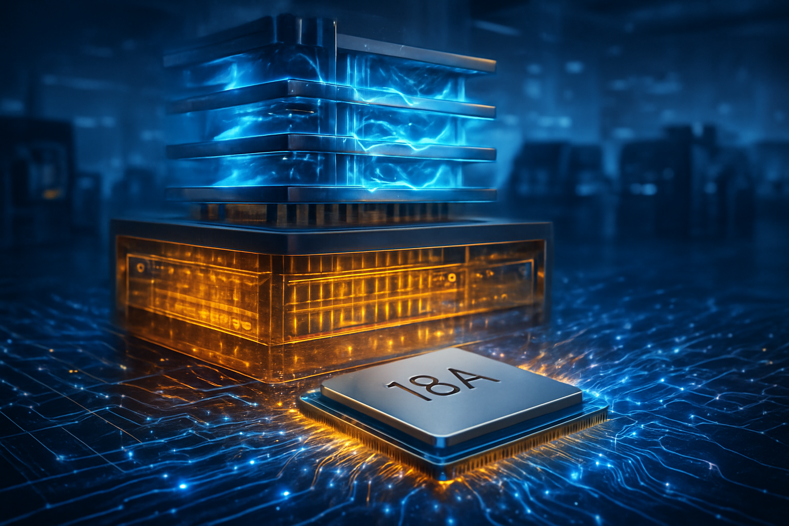
    In a move that signals a tectonic shift in the global semiconductor landscape, reports have emerged as of late December 2025 that Apple Inc. (NASDAQ: AAPL) has successfully entered the critical qualification phase for Intel Corporation’s (NASDAQ: INTC) 18A manufacturing process. This development marks the first time since the "Apple Silicon" transition in 2020 that the iPhone maker has seriously considered a primary manufacturing partner other than Taiwan Semiconductor Manufacturing Company (NYSE: TSM). By qualifying the 1.8nm-class node for future entry-level M-series chips, Apple is effectively ending TSMC’s decade-long monopoly on its high-end processor production, a strategy aimed at diversifying its supply chain and securing domestic U.S. manufacturing capabilities.

    The immediate significance of this partnership cannot be overstated. For Intel, securing Apple as a foundry customer is the ultimate validation of its "five nodes in four years" (5N4Y) turnaround strategy led by CEO Pat Gelsinger. For the broader technology industry, it represents a pivotal moment in the "re-shoring" of advanced chipmaking to American soil. As geopolitical tensions continue to cast a shadow over the Taiwan Strait, Apple’s move to utilize Intel’s Arizona-based "Fab 52" provides a necessary hedge against regional instability while potentially lowering logistics costs and lead times for its highest-volume products, such as the MacBook Air and iPad Pro.

    Technical Breakthroughs: RibbonFET and the PowerVia Advantage

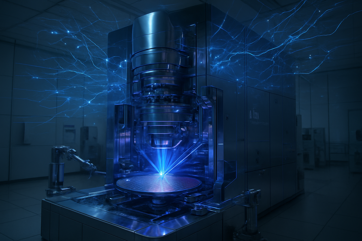
    At the heart of this historic partnership is Intel’s 18A node, a 1.8nm-class process that introduces two of the most significant architectural changes in transistor design in over a decade. The first is RibbonFET, Intel’s proprietary implementation of Gate-All-Around (GAA) technology. Unlike the FinFET transistors used in previous generations, RibbonFET surrounds the conducting channel with the gate on all four sides. This allows for superior electrostatic control, drastically reducing power leakage—a critical requirement for the thin-and-light designs of Apple’s portable devices—while simultaneously increasing switching speeds.

    The second, and perhaps more disruptive, technical milestone is PowerVia, the industry’s first commercial implementation of backside power delivery. By moving power routing to the back of the silicon wafer and keeping signal routing on the front, Intel has solved one of the most persistent bottlenecks in chip design: "IR drop" or voltage loss. According to technical briefings from late 2025, PowerVia allows for a 5% to 10% improvement in cell utilization and a significant boost in performance-per-watt. Reports indicate that Apple has specifically been working with the 18AP (Performance) variant, a specialized version of the node optimized for high-efficiency mobile workloads, which offers an additional 15% to 20% improvement in performance-per-watt over the standard 18A process.

    Initial reactions from the semiconductor research community have been cautiously optimistic. While early reports from partners like Broadcom (NASDAQ: AVGO) and NVIDIA (NASDAQ: NVDA) suggested that Intel’s 18A yields were initially hovering in the 60% to 65% range—below the 70% threshold typically required for high-margin mass production—the news that Apple has received the PDK 0.9.1 GA (Process Design Kit) suggests those hurdles are being cleared. Industry experts note that Apple’s rigorous qualification standards are the "gold seal" of foundry reliability; if Intel can meet Apple’s stringent requirements for the M-series, it proves the 18A node is ready for the most demanding consumer electronics in the world.

    A New Power Dynamic: Disrupting the Foundry Monopoly

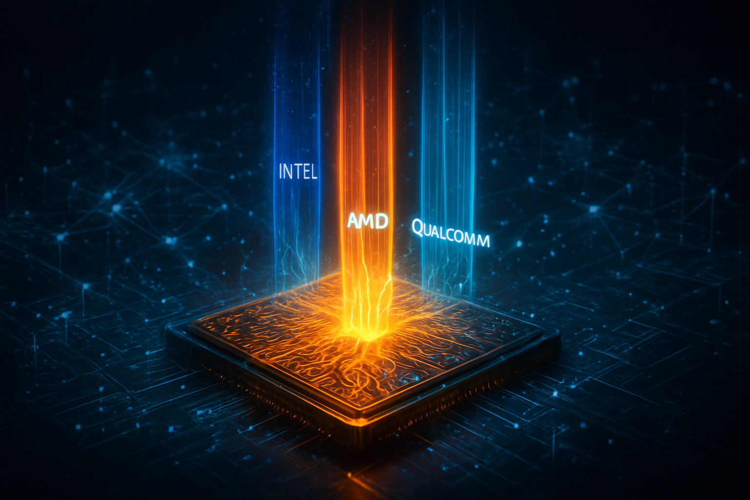
    The strategic implications of this partnership extend far beyond technical specifications. By bringing Intel into the fold, Apple gains immense leverage over TSMC. For years, TSMC has been the sole provider of the world’s most advanced nodes, allowing it to command premium pricing and dictate production schedules. With Intel 18A now a viable alternative, Apple can exert downward pressure on TSMC’s 2nm (N2) pricing. This "dual-foundry" strategy will likely see TSMC retain the manufacturing rights for the high-end "Pro," "Max," and "Ultra" variants of the M-series, while Intel handles the high-volume base models, estimated to reach 15 to 20 million units annually.

    For Intel, this is a transformative win that repositions its Intel Foundry division as a top-tier competitor to TSMC and Samsung (KRX: 005930). Following the news of Apple’s qualification efforts in November 2025, Intel’s stock saw a double-digit surge, reflecting investor confidence that the company can finally monetize its massive capital investments in U.S. manufacturing. The partnership also creates a "halo effect" for Intel Foundry, making it a more attractive option for other tech giants like Microsoft (NASDAQ: MSFT) and Amazon (NASDAQ: AMZN), who are increasingly designing their own custom AI and server silicon.

    However, this development poses a significant challenge to TSMC’s market dominance. While TSMC’s N2 node is still widely considered the gold standard for power efficiency, the geographic concentration of its facilities has become a strategic liability. Apple’s shift toward Intel signals to the rest of the industry that "geopolitical de-risking" is no longer a theoretical preference but a practical manufacturing requirement. If more "fabless" companies follow Apple’s lead, the semiconductor industry could see a more balanced distribution of power between East and West for the first time in thirty years.

    The Broader AI Landscape and the "Made in USA" Mandate

    The Apple-Intel 18A partnership is a cornerstone of the broader trend toward vertical integration and localized supply chains. As AI-driven workloads become the primary focus of consumer hardware, the need for specialized silicon that balances high-performance neural engines with extreme power efficiency has never been greater. Intel’s 18A node is designed with these AI-centric architectures in mind, offering the density required to pack more transistors into the small footprints of next-generation iPads and MacBooks. This fits perfectly into Apple's "Apple Intelligence" roadmap, which demands increasingly powerful on-device processing to handle complex LLM (Large Language Model) tasks without sacrificing battery life.

    This move also aligns with the objectives of the U.S. CHIPS and Science Act. By qualifying a node that will be manufactured in Arizona, Apple is effectively participating in a national effort to secure the semiconductor supply chain. This reduces the risk of global disruptions caused by potential conflicts or pandemics. Comparisons are already being drawn to the 2010s, when Apple transitioned from Samsung to TSMC; that shift redefined the mobile industry, and many analysts believe this return to a domestic partner could have an even greater impact on the future of computing.

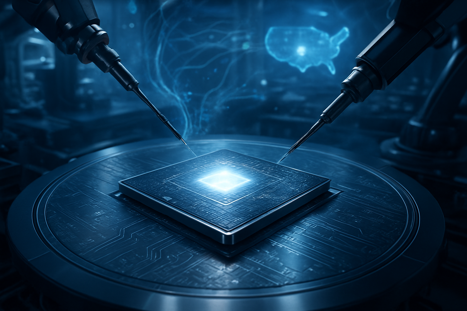
    There are, however, potential concerns regarding the transition. Moving a chip design from TSMC’s ecosystem to Intel’s requires significant engineering resources. Apple’s "qualification" of the node does not yet equal a signed high-volume contract for the entire product line. Some industry skeptics worry that if Intel’s yields do not reach the 70-80% mark by mid-2026, Apple may scale back its commitment, potentially leaving Intel with massive, underutilized capacity. Furthermore, the complexity of PowerVia and RibbonFET introduces new manufacturing risks that could lead to delays if not managed perfectly.

    Looking Ahead: The Road to 2027

    The near-term roadmap for this partnership is clear. Apple is expected to reach a final "go/no-go" decision by the first quarter of 2026, following the release of Intel’s finalized PDK 1.0. If the qualification continues on its current trajectory, the industry expects to see the first Intel-manufactured Apple M-series chips enter mass production in the second or third quarter of 2027. These chips will likely power a refreshed MacBook Air and perhaps a new generation of iPad Pro, marking the commercial debut of "Apple Silicon: Made in America."

    Long-term, this partnership could expand to include iPhone processors (the A-series) or even custom AI accelerators for Apple’s data centers. Experts predict that the success of the 18A node will determine the trajectory of the semiconductor industry for the next decade. If Intel delivers on its performance promises, it could trigger a massive migration of U.S. chip designers back to domestic foundries. The primary challenge remains the execution of High-NA EUV (Extreme Ultraviolet) lithography, a technology Intel is betting heavily on to maintain its lead over TSMC in the sub-2nm era.

    Summary of a Historic Realignment

    The qualification of Intel’s 18A node by Apple represents a landmark achievement in semiconductor engineering and a strategic masterstroke in corporate diplomacy. By bridging the gap between the world’s leading consumer electronics brand and the resurgent American chipmaker, this partnership addresses the two biggest challenges of the modern tech era: the need for unprecedented computational power for AI and the necessity of a resilient, diversified supply chain.

    As we move into 2026, the industry will be watching Intel’s yield rates and Apple’s final production orders with intense scrutiny. The significance of this development in AI history is profound; it provides the physical foundation upon which the next generation of on-device intelligence will be built. For now, the "historic" nature of this partnership is clear: Apple and Intel, once rivals and then distant acquaintances, have found a common cause in the pursuit of silicon sovereignty.


    This content is intended for informational purposes only and represents analysis of current AI and semiconductor developments as of December 29, 2025.

    TokenRing AI delivers enterprise-grade solutions for multi-agent AI workflow orchestration, AI-powered development tools, and seamless remote collaboration platforms. For more information, visit https://www.tokenring.ai/.

  • The Glass Frontier: Intel and Rapidus Lead the Charge into the Next Era of AI Hardware

    The Glass Frontier: Intel and Rapidus Lead the Charge into the Next Era of AI Hardware

    The transition to glass substrates is driven by the failure of organic materials (like ABF and BT resins) to cope with the extreme heat and structural demands of massive AI "superchips." Glass offers a Coefficient of Thermal Expansion (CTE) that closely matches that of silicon (3–7 ppm/°C), which drastically reduces the risk of warpage during the high-temperature manufacturing processes required for advanced 2nm and 1.4nm nodes. Furthermore, glass is an exceptional electrical insulator with significantly lower dielectric loss (Df) and a lower dielectric constant (Dk) than silicon-based interposers. This allows for signal speeds to double while cutting insertion loss in half—a critical requirement for the high-frequency data transfers essential for 5G, 6G, and ultra-fast AI training.

    Technically, the "magic" of glass lies in Through-Glass Vias (TGVs). These microscopic vertical interconnects allow for a 10-fold increase in interconnect density compared to traditional organic substrates. This density enables thousands of Input/Output (I/O) bumps, allowing multiple chiplets—CPUs, GPUs, and High Bandwidth Memory (HBM)—to be packed closer together with minimal latency. At SEMICON Japan in December 2025, Rapidus demonstrated the sheer scale of this potential by unveiling a 600mm x 600mm glass panel-level packaging (PLP) prototype. Unlike traditional 300mm round silicon wafers, these massive square panels can yield up to 10 times more interposers, significantly reducing material waste and enabling the creation of "monster" packages that can house up to 24 HBM4 dies alongside a multi-tile GPU.

    Market Dynamics: A High-Stakes Race for Dominance

    Intel is currently the undisputed leader in the "Glass War," having invested over a decade of R&D into the technology. The company's Arizona-based pilot line is already operational, and Intel is on track to integrate glass substrates into its high-volume manufacturing (HVM) roadmap by late 2026. This head start provides Intel with a significant strategic advantage, potentially allowing them to reclaim the lead in the foundry business by offering packaging capabilities that Taiwan Semiconductor Manufacturing Co. (NYSE: TSM) is not expected to match at scale until 2028 or 2029 with its "CoPoS" (Chip-on-Panel-on-Substrate) initiative.

    However, the competition is intensifying rapidly. Samsung Electronics (KRX: 005930) has fast-tracked its glass substrate development, leveraging its existing expertise in large-scale glass manufacturing from its display division. Samsung is currently building a pilot line at its Sejong facility and aims for a 2026-2027 rollout, potentially positioning itself as a primary alternative for AI giants like NVIDIA and Advanced Micro Devices (NASDAQ: AMD) who are desperate to diversify their supply chains away from a single source. Meanwhile, the emergence of Rapidus as a serious contender with its panel-level prototype suggests that the Japanese semiconductor ecosystem is successfully leveraging its legacy in LCD technology to leapfrog current packaging constraints.

    Redefining the AI Landscape and Moore’s Law

    The wider significance of glass substrates lies in their role as the "enabling platform" for the post-Moore's Law era. As it becomes increasingly difficult to shrink transistors further, the industry has turned to heterogeneous integration—stacking and stitching different chips together. Glass substrates provide the structural integrity needed to build these massive 3D structures. Intel’s stated goal of reaching 1 trillion transistors on a single package by 2030 is virtually impossible without the flatness and thermal stability provided by glass.

    This development also addresses the critical "power wall" in AI data centers. The extreme flatness of glass allows for more reliable implementation of Backside Power Delivery (such as Intel’s PowerVia technology) at the package level. This reduces power noise and improves overall energy efficiency by an estimated 15% to 20%. In an era where AI power consumption is a primary concern for hyperscalers and environmental regulators alike, the efficiency gains from glass substrates could be just as important as the performance gains.

    The Road to 2026 and Beyond

    Looking ahead, the next 12 to 18 months will be focused on solving the remaining engineering hurdles of glass: namely, fragility and handling. While glass is structurally superior once assembled, it is notoriously difficult to handle in a high-speed factory environment without cracking. Companies like Rapidus are working closely with equipment manufacturers to develop specialized "glass-safe" robotic handling systems and laser-drilling techniques for TGVs. If these challenges are met, the shift to 600mm square panels could drop the cost of manufacturing massive AI interposers by as much as 40% by 2027.

    In the near term, expect to see the first commercial glass-packaged chips appearing in high-end server environments. These will likely be specialized AI accelerators or high-end Xeon processors designed for the most demanding scientific computing tasks. As the ecosystem matures, we can anticipate the technology trickling down to consumer-grade high-end gaming GPUs and workstations, where thermal management is a constant struggle. The ultimate goal is a fully standardized glass-based ecosystem that allows for "plug-and-play" chiplet integration from various vendors.

    Conclusion: A New Foundation for Computing

    The move to glass substrates marks the beginning of a new chapter in semiconductor history. It is a transition that validates the industry's shift from "system-on-chip" to "system-in-package." By solving the thermal and density bottlenecks that have plagued organic substrates, Intel and Rapidus are paving the way for a new generation of AI hardware that was previously thought to be physically impossible.

    As we move into 2026, the industry will be watching closely to see if Intel can successfully execute its high-volume rollout and if Rapidus can translate its impressive prototype into a viable manufacturing reality. The stakes are immense; the winner of the glass substrate race will likely hold the keys to the world's most powerful AI systems for the next decade. For now, the "Glass War" is just beginning, and it promises to be the most consequential battle in the tech industry's ongoing evolution.


    This content is intended for informational purposes only and represents analysis of current AI developments.

    TokenRing AI delivers enterprise-grade solutions for multi-agent AI workflow orchestration, AI-powered development tools, and seamless remote collaboration platforms.
    For more information, visit https://www.tokenring.ai/.

  • The High-NA EUV Era Begins: Intel Reclaims the Lead with ASML’s $350M Twinscan EXE:5200B

    The High-NA EUV Era Begins: Intel Reclaims the Lead with ASML’s $350M Twinscan EXE:5200B

    In a move that signals a tectonic shift in the global semiconductor landscape, Intel (NASDAQ: INTC) has officially entered the "High-NA" era. As of late December 2025, the company has successfully completed the installation and acceptance testing of the industry’s first commercial-grade High-NA (Numerical Aperture) Extreme Ultraviolet (EUV) lithography system, the ASML (NASDAQ: ASML) Twinscan EXE:5200B. This $350 million marvel of engineering, now operational at Intel’s D1X research facility in Oregon, represents the cornerstone of Intel's ambitious strategy to leapfrog its competitors and regain undisputed leadership in chip manufacturing by the end of the decade.

    The successful operationalization of the EXE:5200B is more than just a logistical milestone; it is the starting gun for the 1.4nm (14A) process node. By becoming the first chipmaker to integrate High-NA EUV into its production pipeline, Intel is betting that this massive capital expenditure will simplify manufacturing for the most complex AI and high-performance computing (HPC) chips. This development places Intel at the vanguard of the next generation of Moore’s Law, providing a clear path to the 14A node and beyond, while its primary rivals remain more cautious in their adoption of the technology.

    Breaking the 8nm Barrier: The Technical Mastery of the EXE:5200B

    The ASML Twinscan EXE:5200B is a radical departure from the "Low-NA" (0.33 NA) EUV systems that have been the industry standard for the last several years. By increasing the Numerical Aperture from 0.33 to 0.55, the EXE:5200B allows for a significantly finer focus of the EUV light. This enables the machine to print features as small as 8nm, a massive improvement over the 13.5nm limit of previous systems. For Intel, this means the ability to "single-pattern" critical layers of a chip that previously required multiple, complex exposures on older machines. This reduction in process steps not only improves yields but also drastically shortens the manufacturing cycle time for advanced logic.

    Beyond resolution, the EXE:5200B introduces unprecedented precision. The system achieves an overlay accuracy of just 0.7 nanometers—essential for aligning the dozens of microscopic layers that constitute a modern processor. Intel has also been working closely with ASML to tune the machine’s throughput. While the standard output is rated at 175 wafers per hour (WPH), recent reports from the Oregon facility suggest Intel is pushing the system toward 200 WPH. This productivity boost is critical for making the $350 million-plus investment cost-effective for high-volume manufacturing (HVM).

    Industry experts and the semiconductor research community have reacted with a mix of awe and scrutiny. The successful "first light" and subsequent acceptance testing confirm that High-NA EUV is no longer an experimental curiosity but a viable production tool. However, the technical challenges remain immense; the machine requires a vastly more powerful light source and specialized resists to maintain speed at such high resolutions. Intel’s ability to stabilize these variables ahead of its peers is being viewed as a significant engineering win for the company’s "five nodes in four years" roadmap.

    A Strategic Leapfrog: Impact on the Foundry Landscape

    The immediate beneficiaries of this development are the customers of Intel Foundry. By securing the first batch of High-NA machines, Intel is positioning its 14A node as the premier destination for next-generation AI accelerators. Major players like NVIDIA (NASDAQ: NVDA) and Microsoft (NASDAQ: MSFT) are reportedly already evaluating the 14A Process Design Kit (PDK) 0.5, which Intel released earlier this quarter. The promise of higher transistor density and the integration of "PowerDirect"—Intel’s second-generation backside power delivery system—offers a compelling performance-per-watt advantage that is crucial for the power-hungry data centers of 2026 and 2027.

    The competitive implications for TSMC (NYSE: TSM) and Samsung (KRX: 005930) are profound. While TSMC remains the market share leader, it has taken a more conservative "wait-and-see" approach to High-NA, opting instead to extend the life of Low-NA tools through advanced multi-patterning for its upcoming A14 node. TSMC does not expect to move to High-NA for volume production until 2028 or later. Samsung, meanwhile, has faced yield hurdles with its 2nm Gate-All-Around (GAA) process, leading it to delay its own 1.4nm plans until 2029. Intel’s early adoption gives it a potential two-year window where it could offer the most advanced lithography in the world.

    This "leapfrog" strategy is designed to disrupt the existing foundry hierarchy. If Intel can prove that High-NA EUV leads to more reliable, higher-performing chips at the 1.4nm level, it may lure away high-margin business that has traditionally been the exclusive domain of TSMC. For AI startups and tech giants alike, the availability of 1.4nm capacity by 2027 could be the deciding factor in who wins the next phase of the AI hardware race.

    Moore’s Law and the Geopolitical Stakes of Lithography

    The broader significance of the High-NA era extends into the very survival of Moore’s Law. For years, skeptics have predicted the end of transistor scaling due to the physical limits of light and the astronomical costs of fab equipment. The arrival of the EXE:5200B at Intel provides a tangible rebuttal to those claims, demonstrating that while scaling is becoming more expensive, it is not yet impossible. This milestone ensures that the roadmap for AI performance—which is tethered to the density of transistors on a die—remains on an upward trajectory.

    However, this advancement also highlights the growing divide in the semiconductor industry. The $350 million price tag per machine, combined with the billions required to build a compatible "Mega-Fab," means that only a handful of companies—and nations—can afford to compete at the leading edge. This creates a concentration of technological power that has significant geopolitical implications. As the United States seeks to bolster its domestic chip manufacturing through the CHIPS Act, Intel’s High-NA success is being touted as a vital win for national economic security.

    There are also potential concerns regarding the environmental impact of these massive machines. High-NA EUV systems are notoriously power-hungry, requiring specialized cooling and massive amounts of electricity to generate the plasma needed for EUV light. As Intel scales this technology, it will face increasing pressure to balance its manufacturing goals with its corporate sustainability targets. The industry will be watching closely to see if the efficiency gains at the chip level can offset the massive energy footprint of the manufacturing process itself.

    The Road to 14A and 10A: What Lies Ahead

    Looking forward, the roadmap for Intel is clear but fraught with execution risk. The company plans to begin "risk production" on the 14A node in late 2026, with high-volume manufacturing targeted for 2027. Between now and then, Intel must transition the learnings from its Oregon R&D site to its massive production sites in Ohio and Ireland. The success of the 14A node will depend on how quickly Intel can move from "first light" on a single machine to a fleet of EXE:5200B systems running 24/7.

    Beyond 14A, Intel is already eyeing the 10A (1nm) node, which is expected to debut toward the end of the decade. Experts predict that 10A will require even further refinements to High-NA technology, possibly involving "Hyper-NA" systems that ASML is currently conceptualizing. In the near term, the industry is watching for the first "tape-outs" from lead customers on the 14A node, which will provide the first real-world data on whether High-NA delivers the promised performance gains.

    The primary challenge remaining is cost. While Intel has the technical lead, it must prove to its shareholders and customers that the 14A node can be profitable. If the yield rates do not materialize as expected, the massive depreciation costs of the High-NA machines could weigh heavily on the company’s margins. The next 18 months will be the most critical period in Intel’s history as it attempts to turn this technological triumph into a commercial reality.

    A New Chapter in Silicon History

    The installation of the ASML Twinscan EXE:5200B marks the definitive start of the High-NA EUV era. For Intel, it is a bold declaration of intent—a $350 million bet that the path to reclaiming the semiconductor crown runs directly through the most advanced lithography on the planet. By securing the first-mover advantage, Intel has not only validated its internal roadmap but has also forced its competitors to rethink their long-term scaling strategies.

    As we move into 2026, the key takeaways are clear: Intel has the tools, the roadmap, and the early customer interest to challenge the status quo. The significance of this development in AI history cannot be overstated; the chips produced on these machines will power the next generation of large language models, autonomous systems, and scientific simulations. While the road to 1.4nm is paved with technical and financial hurdles, Intel has successfully cleared the first and most difficult gate. The industry now waits to see if the silicon produced in Oregon will indeed change the world.


    This content is intended for informational purposes only and represents analysis of current AI developments.

    TokenRing AI delivers enterprise-grade solutions for multi-agent AI workflow orchestration, AI-powered development tools, and seamless remote collaboration platforms.
    For more information, visit https://www.tokenring.ai/.

  • Intel Reclaims the Silicon Throne: 18A Process Enters High-Volume Manufacturing

    Intel Reclaims the Silicon Throne: 18A Process Enters High-Volume Manufacturing

    In a definitive moment for the global semiconductor industry, Intel Corporation (NASDAQ: INTC) officially announced on December 19, 2025, that its cutting-edge 18A (1.8nm-class) process node has entered High-Volume Manufacturing (HVM). This milestone, achieved at the company’s flagship Fab 52 facility in Chandler, Arizona, represents the successful culmination of the "Five Nodes in Four Years" (5N4Y) roadmap—a daring strategy once viewed with skepticism by industry analysts. The transition to HVM signals that Intel has finally stabilized yields and is ready to challenge the dominance of Asian foundry giants.

    The launch is headlined by the first retail shipments of "Panther Lake" processors, branded as the Core Ultra 300 series. These chips, which power a new generation of AI-native laptops from partners like Dell and HP, serve as the primary vehicle for Intel’s most advanced transistor technologies to date. By hitting this production target before the close of 2025, Intel has not only met its internal deadlines but has also leapfrogged competitors in key architectural innovations, most notably in power delivery and transistor structure.

    The Architecture of Dominance: RibbonFET and PowerVia

    The technical backbone of the 18A node rests on two revolutionary technologies: RibbonFET and PowerVia. RibbonFET is Intel’s implementation of Gate-All-Around (GAA) transistor architecture, which replaces the long-standing FinFET design. By surrounding the conducting channel on all four sides with the gate, RibbonFET provides superior electrostatic control, drastically reducing power leakage while increasing switching speeds. This allows for higher performance at lower voltages, a critical requirement for the thermally constrained environments of modern laptops and high-density data centers.

    However, the true "secret sauce" of 18A is PowerVia, Intel’s proprietary backside power delivery system. Traditionally, power and signal lines are bundled together on the front of a silicon wafer, leading to "routing congestion" and voltage drops. PowerVia moves the power delivery network to the back of the wafer, separating it entirely from the signal lines. Technical data released during the HVM launch indicates that PowerVia reduces IR (voltage) droop by approximately 10% and enables a 6% to 10% frequency gain. Furthermore, by freeing up space on the front side, Intel has achieved a 30% increase in transistor density over its previous Intel 3 node, reaching an estimated 238 million transistors per square millimeter (MTr/mm²).

    Initial reactions from the semiconductor research community have been overwhelmingly positive. Analysts note that while Taiwan Semiconductor Manufacturing Company (NYSE: TSM) still maintains a slight lead in raw transistor density with its N2 node, TSMC’s implementation of backside power is not expected until the N2P or A16 nodes in late 2026. This gives Intel a temporary but significant technical advantage in power efficiency—a metric that has become the primary battleground in the AI era.

    Reshaping the Foundry Landscape

    The move to HVM for 18A is more than a technical victory; it is a strategic earthquake for the foundry market. Under the leadership of CEO Lip-Bu Tan, who took the helm in early 2025, Intel Foundry has been spun off into an independent subsidiary, a move that has successfully courted major tech giants. Microsoft (NASDAQ: MSFT) and Amazon (NASDAQ: AMZN) have already emerged as anchor customers, with Microsoft reportedly utilizing 18A for its "Maia 2" AI accelerators. Perhaps most surprisingly, NVIDIA (NASDAQ: NVDA) finalized a $5 billion strategic investment in Intel late this year, signaling a collaborative shift where the two companies are co-developing custom x86 CPUs for data center applications.

    For years, the industry was a duopoly between TSMC and Samsung Electronics (KRX: 005930). However, Intel’s 18A yields—now stabilized between 60% and 65%—have allowed it to overtake Samsung, whose 2nm-class SF2 process has reportedly struggled with yield bottlenecks near the 40% mark. This positioning makes Intel the clear secondary alternative to TSMC for high-performance silicon. Even Apple (NASDAQ: AAPL), which has historically been exclusive to TSMC for its flagship chips, is reportedly evaluating Intel 18A for its lower-tier Mac and iPad silicon starting in 2027 to diversify its supply chain and mitigate geopolitical risks.

    AI Integration and the Broader Silicon Landscape

    The broader significance of the 18A launch lies in its optimization for Artificial Intelligence. The lead product, Panther Lake, features a next-generation Neural Processing Unit (NPU) capable of over 100 TOPS (Trillions of Operations Per Second). This is specifically architected to handle local generative AI workloads, such as real-time language translation and on-device image generation, without relying on cloud resources. The inclusion of the Xe3 "Celestial" graphics architecture further bolsters this, delivering a 50% improvement in integrated GPU performance over previous generations.

    In the context of the global AI race, 18A provides the hardware foundation necessary for the next leap in "Agentic AI"—autonomous systems that require massive local compute power. This milestone echoes the historical significance of the move to 45nm and High-K Metal Gate technology in 2007, which cemented Intel's dominance for a decade. By successfully navigating the transition to GAA and backside power simultaneously, Intel has proven that the "IDM 2.0" strategy was not just a survival plan, but a roadmap to regaining industry leadership.

    The Road to 14A and Beyond

    Looking ahead, the HVM status of 18A is just the beginning. Intel has already begun installing "High-NA" (High Numerical Aperture) EUV lithography machines from ASML Holding (NASDAQ: ASML) for its upcoming 14A node. Near-term developments include the broad global launch of Panther Lake at CES 2026 and the ramp-up of "Clearwater Forest," a high-core-count server chip designed for the world’s largest data centers.

    Experts predict that the next challenge will be scaling these innovations to the "Angstrom Era" (10A and beyond). While the 18A node has solved the immediate yield crisis, maintaining this momentum will require constant refinement of the High-NA EUV process and further advancements in 3D chip stacking (Foveros Direct). The industry will be watching closely to see if Intel can maintain its yield improvements as it moves toward 14A in 2027.

    Conclusion: A New Chapter for Intel

    The official launch of Intel 18A into high-volume manufacturing marks the most significant turnaround in the company's 57-year history. By successfully delivering RibbonFET and PowerVia, Intel has reclaimed its position at the leading edge of semiconductor manufacturing. The key takeaways are clear: Intel is no longer just a chipmaker, but a world-class foundry capable of serving the most demanding AI and hyperscale customers.

    In the coming months, the focus will shift from manufacturing capability to market adoption. As Panther Lake laptops hit the shelves and Microsoft’s 18A-based AI chips enter the data center, the real-world performance of this silicon will be the ultimate test. For now, the "Silicon Throne" is once again a contested seat, and the competition between Intel and TSMC promises to drive an unprecedented era of innovation in AI hardware.


    This content is intended for informational purposes only and represents analysis of current AI developments.

    TokenRing AI delivers enterprise-grade solutions for multi-agent AI workflow orchestration, AI-powered development tools, and seamless remote collaboration platforms.
    For more information, visit https://www.tokenring.ai/.

  • Intel Closes in on Historic Deal to Manufacture Apple M-Series Chips on 18A Node by 2027

    Intel Closes in on Historic Deal to Manufacture Apple M-Series Chips on 18A Node by 2027

    In what is being hailed as a watershed moment for the global semiconductor industry, Apple Inc. (NASDAQ: AAPL) has reportedly begun the formal qualification process for Intel’s (NASDAQ: INTC) 18A manufacturing node. According to industry insiders and supply chain reports surfacing in late 2025, the two tech giants are nearing a definitive agreement that would see Intel manufacture entry-level M-series silicon for future MacBooks and iPads starting in 2027. This potential partnership marks the first time Intel would produce chips for Apple since the Cupertino-based company famously transitioned to its own ARM-based "Apple Silicon" and severed its processor supply relationship with Intel in 2020.

    The significance of this development cannot be overstated. For Apple, the move represents a strategic pivot toward geopolitical "de-risking," as the company seeks to diversify its advanced-node supply chain away from its near-total reliance on Taiwan Semiconductor Manufacturing Company (NYSE: TSM). For Intel, securing Apple as a foundry customer would serve as the ultimate validation of its "five nodes in four years" roadmap and its ambitious transformation into a world-class contract manufacturer. If the deal proceeds, it would signal a profound "manufacturing renaissance" for the United States, bringing the production of the world’s most advanced consumer electronics back to American soil.

    The Technical Leap: RibbonFET, PowerVia, and the 18AP Variant

    The technical foundation of this deal rests on Intel’s 18A (1.8nm-class) process, which is widely considered the company’s "make-or-break" node. Unlike previous generations, 18A introduces two revolutionary architectural shifts: RibbonFET and PowerVia. RibbonFET is Intel’s implementation of Gate-All-Around (GAA) transistor technology, which replaces the long-standing FinFET design. By surrounding the transistor channel with the gate on all four sides, RibbonFET significantly reduces power leakage and allows for higher drive currents at lower voltages. This is paired with PowerVia, a breakthrough "backside power delivery" system that moves power routing to the reverse side of the wafer. By separating the power and signal lines, Intel has managed to reduce voltage drop to less than 1%, compared to the 6–7% seen in traditional front-side delivery systems, while simultaneously improving chip density.

    According to leaked documents from November 2025, Apple has already received version 0.9.1 GA of the Intel 18AP Process Design Kit (PDK). The "P" in 18AP stands for "Performance," a specialized variant of the 18A node optimized for high-efficiency consumer devices. Reports suggest that 18AP offers a 15% to 20% improvement in performance-per-watt over the standard 18A node, making it an ideal candidate for Apple’s high-volume, entry-level chips like the upcoming M6 or M7 base models. Apple’s engineering teams are currently engaged in intensive architectural modeling to ensure that Intel’s yields can meet the rigorous quality standards that have historically made TSMC the gold standard of the industry.

    The reaction from the AI research and semiconductor communities has been one of cautious optimism. While TSMC remains the leader in volume and reliability, analysts note that Intel’s early lead in backside power delivery gives them a unique competitive edge. Experts suggest that if Intel can successfully scale 18A production at its Fab 52 facility in Arizona, it could match or even exceed the power efficiency of TSMC’s 2nm (N2) node, which Apple is currently using for its flagship "Pro" and "Max" chips.

    Shifting the Competitive Landscape for Tech Giants

    The potential deal creates a new "dual-foundry" reality that fundamentally alters the power dynamics between the world’s largest tech companies. For years, Apple has been TSMC’s most important customer, often receiving exclusive first-access to new nodes. By bringing Intel into the fold, Apple gains immense bargaining power and a critical safety net. This strategy allows Apple to bifurcate its lineup: keeping its highest-end "Pro" and "Max" chips with TSMC in Taiwan and Arizona, while shifting its massive volume of entry-level MacBook Air and iPad silicon to Intel’s domestic fabs.

    This development also has major implications for other industry leaders like Nvidia (NASDAQ: NVDA) and Microsoft (NASDAQ: MSFT). Both companies have already expressed interest in Intel Foundry, but an "Apple-certified" 18A process would likely trigger a stampede of other fabless chip designers toward Intel. If Intel can prove it can handle the volume and complexity of Apple's designs, it effectively removes the "reputational risk" that has hindered Intel Foundry’s growth in its early years. Conversely, for TSMC, the loss of even a portion of Apple’s business represents a significant long-term threat to its market dominance, forcing the Taiwanese firm to accelerate its own US-based expansion and innovate even faster to maintain its lead.

    Furthermore, the split of Intel’s manufacturing business into a separate subsidiary—Intel Foundry—has been a masterstroke in building trust. By maintaining a separate profit-and-loss (P&L) statement and strict data firewalls, Intel has convinced Apple that its proprietary chip designs will remain secure from Intel’s own product divisions. This structural change was a prerequisite for Apple even considering a return to the Intel ecosystem.

    Geopolitics and the Quest for Semiconductor Sovereignty

    Beyond the technical and commercial aspects, the Apple-Intel deal is deeply rooted in the broader geopolitical struggle for semiconductor sovereignty. In the current climate of late 2025, "concentration risk" in the Taiwan Strait has become a primary concern for the US government and Silicon Valley executives alike. Apple’s move is a direct response to this instability, aligning with CEO Tim Cook’s 2025 pledge to invest heavily in a domestic silicon supply chain. By utilizing Intel’s facilities in Oregon and Arizona, Apple is effectively "onshoring" the production of its most popular products, insulating itself from potential trade disruptions or regional conflicts.

    This shift also highlights the success of the US CHIPS and Science Act, which provided the financial framework for Intel’s massive fab expansions. In late 2025, the US government finalized an $8.9 billion equity investment in Intel, effectively cementing the company’s status as a "National Strategic Asset." This government backing ensures that Intel has the capital necessary to compete with the subsidized giants of East Asia. For the first time in decades, the United States is positioned to host the manufacturing of sub-2nm logic chips, a feat that seemed impossible just five years ago.

    However, this "manufacturing renaissance" is not without its critics. Some industry analysts worry that the heavy involvement of the US government could lead to inefficiencies or that Intel may struggle to maintain the relentless pace of innovation required to stay at the leading edge. Comparisons are often made to the early days of the semiconductor industry, but the scale of today’s technology is vastly more complex. The success of the 18A node is not just a corporate milestone for Intel; it is a test case for whether Western nations can successfully reclaim the heights of advanced manufacturing.

    The Road to 2027 and the 14A Horizon

    Looking ahead, the next 12 to 18 months will be critical. Apple is expected to make a final "go/no-go" decision by the first quarter of 2026, following the release of Intel’s finalized 1.0 PDK. If the qualification is successful, Intel will begin the multi-year process of "ramping" the 18A node for mass production. This involves fine-tuning the High-NA EUV (Extreme Ultraviolet) lithography machines that Intel has been pioneered in its Oregon research facilities. These $380 million machines from ASML are the key to reaching even smaller dimensions, and Intel's early adoption of this technology is a major factor in Apple's interest.

    The roadmap doesn't stop at 18A. Reports indicate that Apple is already looking toward Intel’s 14A (1.4nm) process for 2028 and beyond. This suggests that the 2027 deal is not a one-off experiment but the beginning of a long-term strategic partnership. As AI applications continue to demand more compute power and better energy efficiency, the ability to manufacture at the 1.4nm level will be the next great frontier. We can expect to see future M-series chips leveraging these nodes to integrate even more advanced neural engines and on-device AI capabilities that were previously relegated to the cloud.

    The challenges remain significant. Intel must prove it can achieve the high yields necessary for Apple’s massive product launches, which often require tens of millions of chips in a single quarter. Any delays in the 18A ramp could have a domino effect on Apple’s product release cycles. Experts predict that the first half of 2026 will be defined by "yield-watch" reports as the industry monitors Intel's progress in translating laboratory success into factory floor reality.

    A New Era for Silicon Valley

    The potential return of Apple to Intel’s manufacturing plants marks the end of one era and the beginning of another. It signifies a move away from the "fabless" versus "integrated" dichotomy of the past decade and toward a more collaborative, geographically diverse ecosystem. If the 2027 production timeline holds, it will be remembered as the moment the US semiconductor industry regained its footing on the global stage, proving that it could still compete at the absolute bleeding edge of technology.

    For the consumer, this deal promises more efficient, more powerful devices that are less susceptible to global supply chain shocks. For the industry, it provides a much-needed second source for advanced logic, breaking the effective monopoly that TSMC has held over the high-end market. As we move into 2026, all eyes will be on the test wafers coming out of Intel’s Arizona fabs. The stakes could not be higher: the future of the Mac, the viability of Intel Foundry, and the technological sovereignty of the United States all hang in the balance.


    This content is intended for informational purposes only and represents analysis of current AI and semiconductor developments.

    TokenRing AI delivers enterprise-grade solutions for multi-agent AI workflow orchestration, AI-powered development tools, and seamless remote collaboration platforms.
    For more information, visit https://www.tokenring.ai/.

  • Advanced Packaging Becomes the Strategic Battleground for the Next Phase of AI Scaling

    Advanced Packaging Becomes the Strategic Battleground for the Next Phase of AI Scaling

    The Silicon Squeeze: How Advanced Packaging Became the New Front Line in the AI Arms Race

    As of December 26, 2025, the semiconductor industry has reached a pivotal inflection point. For decades, the primary metric of progress was the shrinking of the transistor—the relentless march of Moore’s Law. However, as physical limits and skyrocketing costs make traditional scaling increasingly difficult, the focus has shifted from the chip itself to how those chips are connected. Advanced packaging has emerged as the new strategic battleground, serving as the essential bridge between raw silicon and the massive computational demands of generative AI.

    The magnitude of this shift was cemented earlier this year by a historic $5 billion investment from NVIDIA (NASDAQ: NVDA) into Intel (NASDAQ: INTC). This deal, which saw NVIDIA take a roughly 4% equity stake in its long-time rival, marks the beginning of a "coopetition" era. While NVIDIA continues to dominate the AI GPU market, its growth is currently dictated not by how many chips it can design, but by how many it can package. By securing Intel’s domestic advanced packaging capacity, NVIDIA is attempting to bypass the persistent bottlenecks at TSMC (NYSE: TSM) and insulate itself from the geopolitical risks inherent in the Taiwan Strait.

    The Technical Frontier: CoWoS, Foveros, and the Rise of the Chiplet

    The technical complexity of modern AI hardware has rendered traditional "monolithic" chips—where everything is on one piece of silicon—nearly obsolete for high-end applications. Instead, the industry has embraced heterogeneous integration, a method of stacking various components like CPUs, GPUs, and High Bandwidth Memory (HBM) into a single, high-performance package. The current gold standard is TSMC’s Chip-on-Wafer-on-Substrate (CoWoS), which is the foundation for NVIDIA’s Blackwell architecture. However, CoWoS capacity has remained the primary constraint for AI GPU shipments throughout 2024 and 2025, leading to lead times that have occasionally stretched beyond six months.

    Intel has countered with its own sophisticated toolkit, most notably EMIB (Embedded Multi-die Interconnect Bridge) and Foveros. Unlike CoWoS, which uses a large silicon interposer, EMIB utilizes small silicon bridges embedded directly into the organic substrate, offering a more cost-effective and scalable way to link chiplets. Meanwhile, Foveros Direct 3D represents the cutting edge of vertical integration, using copper-to-copper hybrid bonding to stack logic components with an interconnect pitch of less than 9 microns. This density allows for data transfer speeds and power efficiency that were previously impossible, effectively creating a "3D" computer on a single package.

    Industry experts and the AI research community have reacted to these developments with a mix of awe and pragmatism. "We are no longer just designing circuits; we are designing entire ecosystems within a square inch of silicon," noted one senior researcher at the Advanced Packaging Piloting Facility. The consensus is clear: the "Packaging Wall" is the new barrier to AI scaling. If the interconnects between memory and logic cannot keep up with the processing speed of the GPU, the entire system throttles, rendering the most advanced transistors useless.

    Market Warfare: Diversification and the Foundry Pivot

    The strategic implications of the NVIDIA-Intel alliance are profound. For NVIDIA, the $5 billion investment is a masterclass in supply chain resilience. While TSMC remains its primary manufacturing partner, the reliance on a single source for CoWoS packaging was a systemic vulnerability. By integrating Intel’s packaging services, NVIDIA gains access to a massive, US-based manufacturing footprint just as it prepares to launch its next-generation "Rubin" architecture in 2026. This move also puts pressure on AMD (NASDAQ: AMD), which remains heavily tethered to TSMC’s ecosystem and must now compete for a limited pool of advanced packaging slots.

    For Intel, the deal is a much-needed lifeline and a validation of its "IDM 2.0" strategy. After years of struggling to catch up in transistor density, Intel is positioning its Foundry Services as an open platform for the world's AI giants. The fact that NVIDIA—Intel's fiercest competitor in the data center—is willing to pay $5 billion to use Intel’s packaging is a powerful signal to other players like Qualcomm (NASDAQ: QCOM) and Apple (NASDAQ: AAPL) that Intel’s back-end technology is world-class. It transforms Intel from a struggling chipmaker into a critical infrastructure provider for the entire AI economy.

    This shift is also disrupting the traditional vendor-customer relationship. We are seeing the rise of "bespoke silicon," where companies like Amazon (NASDAQ: AMZN) and Google (NASDAQ: GOOGL) design their own AI accelerators but rely on the specialized packaging capabilities of Intel or TSMC to bring them to life. In this new landscape, the company that controls the assembly line—the "packaging house"—holds as much leverage as the company that designs the chip.

    Geopolitics and the $1.4 Billion CHIPS Act Infusion

    The strategic importance of packaging has not escaped the notice of global superpowers. The U.S. government, through the CHIPS Act, has recognized that having the world's best chip designers is meaningless if the chips must be sent overseas for the final, most critical stages of assembly. In January 2025, the Department of Commerce finalized over $1.4 billion in awards specifically for packaging innovation, including a $1.1 billion grant to Natcast to establish the National Advanced Packaging Manufacturing Program (NAPMP).

    This federal funding is targeted at solving the most difficult physics problems in the industry: power delivery and thermal management. As chips become more densely packed, they generate heat at levels that can melt traditional materials. The NAPMP is currently funding research into advanced glass substrates and silicon photonics—using light instead of electricity to move data between chiplets. These technologies are seen as essential for the next decade of AI growth, where the energy cost of moving data will outweigh the cost of computing it.

    Compared to previous milestones in AI, such as the transition to 7nm or 5nm nodes, the "Packaging Era" is more about efficiency and integration than raw speed. It is a recognition that the AI revolution is as much a challenge of materials science and mechanical engineering as it is of software and algorithms. However, this transition also raises concerns about further consolidation in the industry. The extreme capital requirements for advanced packaging facilities—often costing upwards of $20 billion—mean that only a handful of companies can afford to play at the highest level, potentially stifling smaller innovators.

    The Horizon: Glass Substrates and the 2026 Roadmap

    Looking ahead, the next two years will be defined by the transition to glass substrates. Unlike traditional organic materials, glass offers superior flatness and thermal stability, allowing for even tighter interconnects and larger package sizes. Intel is currently leading the charge in this area, with plans to integrate glass substrates into high-volume manufacturing by late 2026. This could provide a significant leap in performance for AI models that require massive amounts of "on-package" memory to function efficiently.

    We also expect to see the "chipletization" of everything. By 2027, it is predicted that even mid-range consumer devices will utilize advanced packaging to combine specialized AI "tiles" with standard processing cores. This will enable a new generation of edge AI applications, from real-time holographic communication to autonomous robotics, all running on hardware that is more power-efficient than today’s flagship GPUs. The challenge remains yield: as packages become more complex, a single defect in one chiplet can ruin the entire assembly, making process control and metrology the next major areas of investment for companies like Applied Materials (NASDAQ: AMAT).

    Conclusion: A New Era of Hardware Sovereignty

    The emergence of advanced packaging as a strategic battleground marks the end of the "monolithic" era of computing. The $5 billion handshake between NVIDIA and Intel, coupled with the aggressive intervention of the U.S. government, signals that the future of AI will be built on the back-end. The ability to stack, connect, and cool silicon has become the ultimate differentiator in a world where data is the new oil and compute is the new currency.

    As we move into 2026, the industry's focus will remain squarely on capacity. Watch for the ramp-up of Intel’s 18A node and the first shipments of NVIDIA’s Rubin GPUs, which will serve as the ultimate test for these new packaging technologies. The companies that successfully navigate this "Silicon Squeeze" will not only lead the AI market but will also define the technological sovereignty of nations in the decades to come.


    This content is intended for informational purposes only and represents analysis of current AI developments.

    TokenRing AI delivers enterprise-grade solutions for multi-agent AI workflow orchestration, AI-powered development tools, and seamless remote collaboration platforms.
    For more information, visit https://www.tokenring.ai/.

  • The AI PC Revolution: Intel, AMD, and Qualcomm Battle for NPU Performance Leadership in 2025

    The AI PC Revolution: Intel, AMD, and Qualcomm Battle for NPU Performance Leadership in 2025

    As 2025 draws to a close, the personal computing landscape has undergone its most radical transformation since the transition to mobile. What began as a buzzword a year ago has solidified into a hardware arms race, with Qualcomm (NASDAQ: QCOM), AMD (NASDAQ: AMD), and Intel (NASDAQ: INTC) locked in a fierce battle for dominance over the "AI PC." The defining metric of this era is no longer just clock speed or core count, but Neural Processing Unit (NPU) performance, measured in Tera Operations Per Second (TOPS). This shift has moved artificial intelligence from the cloud directly onto the silicon sitting on our desks and laps.

    The implications are profound. For the first time, high-performance Large Language Models (LLMs) and complex generative AI tasks are running locally without the latency or privacy concerns of data centers. With the holiday shopping season in full swing, the choice for consumers and enterprises alike has come down to which architecture can best handle the increasingly "agentic" nature of modern software. The results are reshaping market shares and challenging the long-standing x86 hegemony in the Windows ecosystem.

    The Silicon Showdown: 80 TOPS and the 70-Billion Parameter Milestone

    The technical achievements of late 2025 have shattered previous expectations for mobile silicon. Qualcomm’s Snapdragon X2 Elite has emerged as the raw performance leader in dedicated AI processing, featuring a Hexagon NPU that delivers a staggering 80 TOPS. Built on a 3nm process, the X2 Elite’s architecture is designed for "always-on" AI, allowing for real-time, multi-modal translation and sophisticated on-device video editing that was previously impossible without a high-end discrete GPU. Qualcomm’s 228 GB/s memory bandwidth further ensures that these AI workloads don't bottleneck the rest of the system.

    AMD has taken a different but equally potent approach with its Ryzen AI Max, colloquially known as "Strix Halo." While its NPU is rated at 50 TOPS, the chip’s secret weapon is its massive unified memory architecture and integrated RDNA 3.5 graphics. With up to 96GB of allocatable VRAM and 256 GB/s of bandwidth, the Ryzen AI Max is the first consumer chip capable of running a 70-billion-parameter model, such as Llama 3.3, entirely locally at usable speeds. Industry experts have noted that AMD’s ability to maintain 3–4 tokens per second on such massive models effectively turns a standard laptop into a localized AI research station.

    Intel, meanwhile, has staged a massive technological comeback with its Panther Lake architecture, the first major consumer line built on the Intel 18A (1.8nm) process node. While its NPU matches AMD at 50 TOPS, Intel has focused on "Platform TOPS"—the combined power of the CPU, NPU, and the new Xe3 "Celestial" GPU. Together, Panther Lake delivers a total of 180 TOPS of AI throughput. This heterogenous computing approach allows Intel-based machines to handle a wide variety of AI tasks, from low-power background noise cancellation to high-intensity image generation, with unprecedented efficiency.

    Strategic Shifts and the End of the "Wintel" Monopoly

    This technological leap is causing a seismic shift in the competitive landscape. Qualcomm’s success with the X2 Elite has finally broken the x86 stranglehold on the high-end Windows market, with the company projected to capture nearly 25% of the premium laptop segment by the end of the year. Major manufacturers like Dell, HP, and Lenovo have moved to a "tri-platform" strategy, offering flagship models in Qualcomm, AMD, and Intel flavors to cater to different AI needs. This diversification has reduced the leverage Intel once held over the PC ecosystem, forcing the silicon giant to innovate at a faster pace than seen in the last decade.

    For the major AI labs and software developers, this hardware revolution is a massive boon. Companies like Microsoft, Adobe, and Google are no longer restricted by the costs of cloud inference for every AI feature. Instead, they are shipping "local-first" versions of their tools. This shift is disrupting the traditional SaaS model; if a user can run a 70B parameter assistant locally on an AMD Ryzen AI Max, the incentive to pay for a monthly cloud-based AI subscription diminishes. This is forcing a pivot toward "hybrid AI" services that only use the cloud for the most extreme computational tasks.

    Furthermore, the power of these integrated AI engines is effectively killing the market for entry-level and mid-range discrete GPUs. With Intel’s Xe3 and AMD’s RDNA 3.5 graphics providing enough horsepower for both 1080p gaming and significant AI acceleration, the need for a separate NVIDIA (NASDAQ: NVDA) card in a standard productivity or creator laptop has vanished. This has forced NVIDIA to refocus its consumer efforts even more heavily on the ultra-high-end enthusiast and professional workstation markets.

    A Fundamental Reshaping of the Computing Landscape

    The "AI PC" is more than a marketing gimmick; it represents a fundamental shift in how humans interact with computers. We are moving away from the "point-and-click" era into the "intent-based" era. With 50 to 80 TOPS of local NPU power, operating systems are becoming proactive. Windows 12 (and its subsequent updates in 2025) now uses these NPUs to index every action, document, and meeting, allowing for a "Recall" feature that is entirely private and locally searchable. The broader significance lies in the democratization of high-level AI; tools that were once the province of data scientists are now available to any student with a modern laptop.

    However, this transition has not been without concerns. The "AI tax" on hardware—the increased cost of high-bandwidth memory and specialized silicon—has pushed the average selling price of laptops higher in 2025. There are also growing debates regarding the environmental impact of local AI; while it saves data center energy, the aggregate power consumption of millions of NPUs running local models is significant. Despite these challenges, the milestone of running 70B parameter models on a consumer device is being compared to the introduction of the graphical user interface in terms of its long-term impact on productivity.

    The Horizon: Agentic OS and the Path to 200+ TOPS

    Looking ahead to 2026, the industry is already teasing the next generation of silicon. Rumors suggest that the successor to the Snapdragon X2 Elite will aim for 120 TOPS on the NPU alone, while Intel’s "Nova Lake" is expected to further refine the 18A process for even higher efficiency. The near-term goal for all three players is to enable "Full-Day Agentic Computing," where an AI assistant can run in the background for 15+ hours on a single charge, managing a user's entire digital workflow without ever needing to ping a remote server.

    The next major challenge will be memory. While 32GB of RAM has become the new baseline for AI PCs in 2025, the demand for 64GB and 128GB configurations is skyrocketing as users seek to run even larger models locally. We expect to see new memory standards, perhaps LPDDR6, tailored specifically for the high-bandwidth needs of NPUs. Experts predict that by 2027, the concept of a "non-AI PC" will be as obsolete as a computer without an internet connection.

    Conclusion: The New Standard for Personal Computing

    The battle between Intel, AMD, and Qualcomm in 2025 has cemented the NPU as the heart of the modern computer. Qualcomm has proven that ARM can lead in raw AI performance, AMD has shown that unified memory can bring massive models to the masses, and Intel has demonstrated that its manufacturing prowess with 18A can still set the standard for total platform throughput. Together, they have initiated a revolution that makes the PC more personal, more capable, and more private than ever before.

    As we move into 2026, the focus will shift from "What can the hardware do?" to "What will the software become?" With the hardware foundation now firmly in place, the stage is set for a new generation of AI-native applications that will redefine work, creativity, and communication. For now, the winner of the 2025 AI PC war is the consumer, who now holds more computational power in their backpack than a room-sized supercomputer did just a few decades ago.


    This content is intended for informational purposes only and represents analysis of current AI developments.

    TokenRing AI delivers enterprise-grade solutions for multi-agent AI workflow orchestration, AI-powered development tools, and seamless remote collaboration platforms.
    For more information, visit https://www.tokenring.ai/.

  • High-NA EUV Era Begins: Intel Deploys First ASML Tool as China Signals EUV Prototype Breakthrough

    High-NA EUV Era Begins: Intel Deploys First ASML Tool as China Signals EUV Prototype Breakthrough

    The global semiconductor landscape reached a historic inflection point in late 2025 as Intel Corporation (NASDAQ: INTC) announced the successful installation and acceptance testing of the industry's first commercial High-Numerical Aperture (High-NA) Extreme Ultraviolet (EUV) lithography tool. The machine, a $350 million ASML (NASDAQ: ASML) Twinscan EXE:5200B, represents the most advanced piece of manufacturing equipment ever created, signaling the start of the "Angstrom Era" in chip production. By securing the first of these massive systems, Intel aims to leapfrog its rivals and reclaim the crown of transistor density and power efficiency.

    However, the Western technological lead is facing an unprecedented challenge from the East. Simultaneously, reports have emerged from Shenzhen, China, indicating that a domestic research consortium has validated a working EUV prototype. This breakthrough, part of a state-sponsored "Manhattan Project" for semiconductors, suggests that China is making rapid progress in bypassing US-led export bans. While the Chinese prototype is not yet ready for high-volume manufacturing, its existence marks a significant milestone in Beijing’s quest for technological sovereignty, with a stated goal of producing domestic EUV-based processors by 2028.

    The Technical Frontier: 1.4nm and the High-NA Advantage

    The ASML Twinscan EXE:5200B is a marvel of engineering, standing nearly two stories tall and requiring multiple Boeing 747s for transport. The defining feature of this tool is its Numerical Aperture (NA), which has been increased from the 0.33 of standard EUV machines to 0.55. This jump in NA allows for an 8nm resolution, a significant improvement over the 13.5nm limit of previous generations. For Intel, this means the ability to print features for its upcoming 14A (1.4nm) node using "single-patterning." Previously, achieving such small dimensions required "multi-patterning," a process where a single layer is printed multiple times, which increases the risk of defects and dramatically raises production costs.

    Initial reactions from the semiconductor research community have been a mix of awe and cautious optimism. Dr. Aris Silzars, a veteran industry analyst, noted that the EXE:5200B’s throughput—capable of processing 175 to 200 wafers per hour—is the "holy grail" for making the 1.4nm node economically viable. The tool also boasts an overlay accuracy of 0.7 nanometers, a precision equivalent to hitting a golf ball on the moon from Earth. Experts suggest that by adopting High-NA early, Intel is effectively "de-risking" its roadmap for the next decade, while competitors like Taiwan Semiconductor Manufacturing Company (NYSE: TSM) and Samsung Electronics (KRX: 005930) have opted for a more conservative approach, extending the life of standard EUV tools through complex multi-patterning techniques.

    In contrast, the Chinese prototype developed in Shenzhen utilizes a different technical path. While ASML uses Laser-Produced Plasma (LPP) to generate EUV light, the Chinese team, reportedly led by engineers from Huawei and various state-funded institutes, has successfully demonstrated a Laser-Induced Discharge Plasma (LDP) source. Though currently producing only 100W–150W of power—roughly half of what is needed for high-speed commercial production—it proves that China has solved the fundamental physics of EUV light generation. This "Manhattan Project" approach has involved a massive mobilization of talent, including former ASML and Nikon (OTC: NINNY) engineers, to reverse-engineer the complex reflective optics and light sources that were previously thought to be decades out of reach for domestic Chinese firms.

    Strategic Maneuvers: The Battle for Lithography Leadership

    Intel’s aggressive move to install the EXE:5200B is a clear strategic play to regain the manufacturing lead it lost over the last decade. By being the first to master High-NA, Intel (NASDAQ: INTC) provides its foundry customers with a unique value proposition: the ability to manufacture the world’s most advanced AI and mobile chips with fewer processing steps and higher yields. This development puts immense pressure on TSMC (NYSE: TSM), which has dominated the 3nm and 5nm markets. If Intel can successfully ramp up the 14A node by 2026 or 2027, it could disrupt the current foundry hierarchy and attract major clients like Apple and Nvidia that have traditionally relied on Taiwanese fabrication.

    The competitive implications extend far beyond the United States and Taiwan. China's breakthrough in Shenzhen represents a direct challenge to the efficacy of the U.S. Department of Commerce's export controls. For years, the denial of EUV tools to Chinese firms like SMIC was considered a "hard ceiling" that would prevent China from progressing beyond the 7nm or 5nm nodes. The validation of a domestic EUV prototype suggests that this ceiling is cracking. If China can scale this technology, it would not only secure its own supply chain but also potentially offer a cheaper, state-subsidized alternative to the global market, disrupting the high-margin business models of Western equipment makers.

    Furthermore, the emergence of the Chinese "Manhattan Project" has sparked a new arms race in lithography. Companies like Canon (NYSE: CAJ) are attempting to bypass EUV altogether with "nanoimprint" lithography, but the industry consensus remains that EUV is the only viable path for sub-2nm chips. Intel’s first-mover advantage with the EXE:5200B creates a "financial and technical moat" that may be too expensive for smaller players to cross, potentially consolidating the leading-edge market into a triopoly of Intel, TSMC, and Samsung.

    Geopolitical Stakes and the Future of Moore’s Law

    The simultaneous announcements from Oregon and Shenzhen highlight the intensifying "Chip War" between the U.S. and China. This is no longer just a corporate competition; it is a matter of national security and economic survival. The High-NA EUV tools are the "printing presses" of the modern era, and the nation that controls them controls the future of Artificial Intelligence, autonomous systems, and advanced weaponry. Intel's success is seen as a validation of the CHIPS Act and the U.S. strategy to reshore critical manufacturing.

    However, the broader AI landscape is also at stake. As AI models grow in complexity, the demand for more transistors per square millimeter becomes insatiable. High-NA EUV is the only technology currently capable of sustaining the pace of Moore’s Law—the observation that the number of transistors on a microchip doubles about every two years. Without the precision of the EXE:5200B, the industry would likely face a "performance wall," where the energy costs of running massive AI data centers would become unsustainable.

    The potential concerns surrounding this development are primarily geopolitical. If China succeeds in its 2028 goal of domestic EUV processors, it could render current sanctions obsolete and lead to a bifurcated global tech ecosystem. We are witnessing the end of a globalized semiconductor supply chain and the birth of two distinct, competing stacks: one led by the U.S. and ASML, and another led by China’s centralized "whole-of-nation" effort. This fragmentation could lead to higher costs for consumers and a slower pace of global innovation as research is increasingly siloed behind national borders.

    The Road to 2028: What Lies Ahead

    Looking forward, the next 24 to 36 months will be critical for both Intel and the Chinese consortium. For Intel (NASDAQ: INTC), the challenge is transitioning from "installation" to "yield." It is one thing to have a $350 million machine; it is another to produce millions of perfect chips with it. The industry will be watching closely for the first "tape-outs" of the 14A node, which will serve as the litmus test for High-NA's commercial viability. If Intel can prove that High-NA reduces the total cost of ownership per transistor, it will have successfully executed one of the greatest comebacks in industrial history.

    In China, the focus will shift from the Shenzhen prototype to the more ambitious "Steady-State Micro-Bunching" (SSMB) project in Xiong'an. Unlike the standalone ASML tools, SSMB uses a particle accelerator to generate EUV light for an entire cluster of lithography machines. If this centralized light-source model works, it could fundamentally change the economics of chipmaking, allowing China to build "EUV factories" that are more scalable than anything in the West. Experts predict that while 2028 is an aggressive target for domestic EUV processors, a 2030 timeline for stable production is increasingly realistic.

    The immediate challenges remain daunting. For Intel, the "reticle stitching" required by High-NA’s smaller field size presents a significant software and design hurdle. For China, the lack of a mature ecosystem for EUV photoresists and masks—the specialized chemicals and plates used in the printing process—could still stall their progress even if the light source is perfected. The race is now a marathon of engineering endurance.

    Conclusion: A New Chapter in Silicon History

    The installation of the ASML Twinscan EXE:5200B at Intel and the emergence of China’s EUV prototype represent the start of a new chapter in silicon history. We have officially moved beyond the era where 0.33 NA lithography was the pinnacle of human achievement. The "High-NA Era" promises to push computing power to levels previously thought impossible, enabling the next generation of AI breakthroughs that will define the late 2020s and beyond.

    As we move into 2026, the significance of these developments cannot be overstated. Intel has reclaimed a seat at the head of the technical table, but China has proven that it will not be easily sidelined. The "Manhattan Project" for chips is no longer a theoretical threat; it is a functional reality that is beginning to produce results. The long-term impact will be a world where the most advanced technology is both a tool for incredible progress and a primary instrument of geopolitical power.

    In the coming weeks and months, industry watchers should look for announcements regarding Intel's first 14A test chips and any further technical disclosures from the Shenzhen research group. The battle for the 1.4nm node has begun, and the stakes have never been higher.


    This content is intended for informational purposes only and represents analysis of current AI developments.

    TokenRing AI delivers enterprise-grade solutions for multi-agent AI workflow orchestration, AI-powered development tools, and seamless remote collaboration platforms.
    For more information, visit https://www.tokenring.ai/.

  • Intel’s 18A Node Hits Volume Production at Fab 52 as Yields Stabilize for Panther Lake Ramp

    Intel’s 18A Node Hits Volume Production at Fab 52 as Yields Stabilize for Panther Lake Ramp

    Intel Corporation (NASDAQ:INTC) has officially reached a historic milestone in the semiconductor race, announcing that its 18A (1.8nm-class) process node has entered high-volume manufacturing (HVM) at the newly operational Fab 52 in Arizona. This achievement marks the successful completion of CEO Pat Gelsinger’s ambitious "five nodes in four years" roadmap, positioning the American chipmaker as the first in the world to deploy 2nm-class technology at scale. As of late December 2025, the 18A node is powering the initial production ramp of the "Panther Lake" processor family, a critical product designed to cement Intel’s leadership in the burgeoning AI PC market.

    The transition to volume production at the $30 billion Fab 52 facility is a watershed moment for the U.S. semiconductor industry. While the journey to 18A was marked by skepticism from Wall Street and technical hurdles, internal reports now indicate that manufacturing yields have stabilized significantly. After trailing the mature yields of Taiwan Semiconductor Manufacturing Co. (NYSE:TSM) earlier in the year, Intel’s 18A process has shown a steady improvement of approximately 7% per month. Yields reached the 60-65% range in November, and the company is currently on track to hit its 70% target by the close of 2025, providing the necessary economic foundation for both internal products and external foundry customers.

    The Architecture of Leadership: RibbonFET and PowerVia

    The 18A node represents more than just a shrink in transistor size; it introduces the most significant architectural shifts in semiconductor manufacturing in over a decade. At the heart of 18A are two foundational technologies: RibbonFET and PowerVia. RibbonFET is Intel’s implementation of Gate-All-Around (GAA) transistors, which replaces the long-standing FinFET design. By wrapping the gate around all four sides of the transistor channel, RibbonFET provides superior electrostatic control, drastically reducing power leakage and allowing for higher drive currents. This results in a reported 25% performance-per-watt improvement over previous generations, a vital metric for AI-heavy workloads that demand extreme efficiency.

    Complementing RibbonFET is PowerVia, Intel’s industry-first commercialization of backside power delivery. Traditionally, power and signal lines are bundled together on the front of a chip, leading to "voltage droop" and routing congestion. PowerVia moves the power delivery network to the back of the silicon wafer, separating it from the signal lines. This decoupling allows for a 10% reduction in IR (voltage) droop and frees up significant space for signal routing, enabling a 0.72x area reduction compared to the Intel 3 node. This dual-innovation approach has allowed Intel to leapfrog competitors who are not expected to integrate backside power until their 2nm or sub-2nm nodes in 2026.

    Industry experts have noted that the stabilization of 18A yields is a testament to Intel’s aggressive use of ASML (NASDAQ:ASML) Twinscan NXE:3800E Low-NA EUV lithography systems. While the industry initially questioned Intel’s decision to skip High-NA EUV for the 18A node in favor of refined Low-NA techniques, the current volume ramp suggests the gamble has paid off. By perfecting the manufacturing process on existing equipment, Intel has managed to reach HVM ahead of TSMC’s N2 (2nm) schedule, which is not expected to see similar volume until mid-to-late 2026.

    Shifting the Competitive Landscape: Intel Foundry vs. The World

    The successful ramp of 18A at Fab 52 has immediate and profound implications for the global foundry market. For years, TSMC has held a near-monopoly on leading-edge manufacturing, serving giants like Apple (NASDAQ:AAPL) and NVIDIA (NASDAQ:NVDA). However, Intel’s progress is already drawing significant interest from "anchor" foundry customers. Microsoft (NASDAQ:MSFT) and Amazon (NASDAQ:AMZN) have already committed to using the 18A node for their custom AI silicon, seeking to diversify their supply chains and reduce their total reliance on Taiwanese fabrication.

    The competitive pressure is now squarely on Samsung (KRX:005930) and TSMC. While Samsung was the first to introduce GAA at 3nm, it struggled with yield issues that prevented widespread adoption. Intel’s ability to hit 60-65% yields on a more advanced 1.8nm-class node puts it in a prime position to capture market share from customers who are wary of Samsung’s consistency. For TSMC, the threat is more strategic; Intel is no longer just a designer of CPUs but a direct competitor in the high-margin foundry business. If Intel can maintain its 7% monthly yield improvement trajectory, it may offer a cost-competitive alternative to TSMC’s upcoming N2 node by the time the latter reaches volume.

    Furthermore, the "Panther Lake" ramp serves as a crucial internal proof of concept. By manufacturing 70% of the Panther Lake die area in-house on 18A, Intel is reducing its multi-billion dollar payments to external foundries. This vertical integration—the "IDM 2.0" strategy—is designed to improve Intel’s gross margins, which have been under pressure during this intensive capital expenditure phase. If Panther Lake meets its performance targets in the retail market this month, it will signal to the entire industry that Intel’s manufacturing engine is once again firing on all cylinders.

    Geopolitics and the AI Infrastructure Era

    The broader significance of 18A production at Fab 52 cannot be overstated in the context of global technopolitics. As the U.S. government seeks to "re-shore" critical technology through the CHIPS and Science Act, Intel’s Arizona facility stands as the premier example of domestic leading-edge manufacturing. The 18A node is already the designated process for the Department of Defense’s "Secure Enclave" program, ensuring that the next generation of American defense and intelligence hardware is built on home soil. This creates a "moat" for Intel that is as much about national security as it is about transistor density.

    In the AI landscape, the 18A node arrives at a pivotal moment. The current "AI PC" trend requires processors that can handle complex neural network tasks locally without sacrificing battery life. The efficiency gains from RibbonFET and PowerVia are specifically tailored for these use cases. By being the first to reach 2nm-class production, Intel is providing the hardware foundation for the next wave of generative AI applications, potentially shifting the balance of power in the laptop and workstation markets back in its favor after years of gains by ARM-based (NASDAQ:ARM) competitors.

    This milestone also marks the end of an era of uncertainty for Intel. The "five nodes in four years" promise was often viewed as a marketing slogan rather than a realistic engineering goal. By delivering 18A in volume by the end of 2025, Intel has restored its credibility with investors and partners alike. This achievement echoes the "Tick-Tock" era of Intel’s past dominance, suggesting that the company has finally overcome the 10nm and 7nm delays that plagued it for nearly a decade.

    The Road to 14A and High-NA EUV

    Looking ahead, the success of 18A is the springboard for Intel’s next ambitious phase: the 14A (1.4nm) node. While 18A utilized refined Low-NA EUV, the 14A node will be the first to implement ASML’s High-NA EUV lithography at scale. Intel has already taken delivery of the first High-NA machines at its Oregon R&D site, and the lessons learned from the 18A ramp at Fab 52 will be instrumental in perfecting the next generation of patterning.

    In the near term, the industry will be watching the ramp of "Clearwater Forest," the 18A-based Xeon processor scheduled for early 2026. While Panther Lake addresses the consumer market, Clearwater Forest will be the true test of 18A’s viability in the high-stakes data center market. If Intel can deliver superior performance-per-watt in the server space, it could halt the market share erosion it has faced at the hands of AMD (NASDAQ:AMD).

    Challenges remain, particularly in scaling the 18A process to meet the diverse needs of dozens of foundry customers, each with unique design rules. However, the current trajectory suggests that Intel is well-positioned to reclaim the "manufacturing crown" by 2026. Analysts predict that if yields hit the 70% target by early 2026, Intel Foundry could become a profitable standalone entity sooner than originally anticipated, fundamentally altering the economics of the semiconductor industry.

    A New Chapter for Silicon

    The commencement of volume production at Fab 52 is more than just a corporate achievement; it is a signal that the semiconductor industry remains a field of rapid, disruptive innovation. Intel’s 18A node combines the most advanced transistor architecture with a revolutionary power delivery system, setting a new benchmark for what is possible in silicon. As Panther Lake chips begin to reach consumers this month, the world will get its first taste of the 1.8nm era.

    The key takeaways from this development are clear: Intel has successfully navigated its most difficult technical transition in history, the U.S. has regained a foothold in leading-edge manufacturing, and the race for AI hardware supremacy has entered a new, more competitive phase. The next few months will be critical as Intel moves from "stabilizing" yields to "optimizing" them for a global roster of clients.

    For the tech industry, the message is undeniable: the "Intel is back" narrative is no longer just a projection—it is being etched into silicon in the Arizona desert. As 2025 draws to a close, the focus shifts from whether Intel can build the future to how fast they can scale it.


    This content is intended for informational purposes only and represents analysis of current AI and semiconductor developments.

    TokenRing AI delivers enterprise-grade solutions for multi-agent AI workflow orchestration, AI-powered development tools, and seamless remote collaboration platforms.
    For more information, visit https://www.tokenring.ai/.

  • The Race to Silicon Sovereignty: TSMC Unveils Roadmap to 1nm and Accelerates Arizona Expansion

    The Race to Silicon Sovereignty: TSMC Unveils Roadmap to 1nm and Accelerates Arizona Expansion

    As the world enters the final months of 2025, the global semiconductor landscape is undergoing a seismic shift. Taiwan Semiconductor Manufacturing Company (NYSE: TSM), the world’s largest contract chipmaker, has officially detailed its roadmap for the "Angstrom Era," centering on the highly anticipated A14 (1.4nm) process node. This announcement comes at a pivotal moment as TSMC confirms that its N2 (2nm) node has reached full-scale mass production in Taiwan, marking the industry’s first successful transition to nanosheet transistor architecture at volume.

    The roadmap is not merely a technical achievement; it is a strategic fortification of TSMC's dominance. By outlining a clear path to 1.4nm production by 2028 and simultaneously accelerating its manufacturing footprint in the United States, TSMC is signaling its intent to remain the indispensable partner for the AI revolution. With the demand for high-performance computing (HPC) and energy-efficient AI silicon reaching unprecedented levels, the move to A14 represents the next frontier in Moore’s Law, promising to pack more than a trillion transistors on a single package by the end of the decade.

    Technical Mastery: The A14 Node and the High-NA EUV Gamble

    The A14 node, which TSMC expects to enter risk production in late 2027 followed by volume production in 2028, represents a refined evolution of the Gate-All-Around (GAA) nanosheet transistors debuting with the current N2 node. Technically, A14 is projected to deliver a 15% performance boost at the same power level or a 25–30% reduction in power consumption compared to N2. Logic density is also expected to jump by over 20%, a critical metric for the massive GPU clusters required by next-generation LLMs. To achieve this, TSMC is introducing "NanoFlex Pro," a design-technology co-optimization (DTCO) tool that allows chip designers from companies like NVIDIA (NASDAQ: NVDA) and Apple (NASDAQ: AAPL) to mix high-performance and high-density cells within a single block, maximizing efficiency.

    Perhaps the most discussed aspect of the A14 roadmap is TSMC’s decision to bypass High-NA EUV (Extreme Ultraviolet) lithography for the initial phase of 1.4nm production. While Intel (NASDAQ: INTC) has aggressively adopted the $380 million machines from ASML (NASDAQ: ASML) for its 14A node, TSMC has opted to stick with its proven 0.33-NA EUV tools combined with advanced multi-patterning. TSMC leadership argued in late 2025 that the economic maturity and yield stability of standard EUV outweigh the resolution benefits of High-NA for the first generation of A14. This "yield-first" strategy aims to avoid the production bottlenecks that have historically plagued aggressive lithography transitions, ensuring that high-volume clients receive predictable delivery schedules.

    The Competitive Chessboard: Fending Off Intel and Samsung

    The A14 announcement sets the stage for a high-stakes showdown in the late 2020s. Intel’s "IDM 2.0" strategy is currently in its most critical phase, with the company betting that its early adoption of High-NA EUV and "PowerVia" backside power delivery will allow its 14A node to leapfrog TSMC by 2027. Meanwhile, Samsung (KRX: 005930) is aggressively marketing its SF1.4 node, leveraging its longer experience with GAA transistors—which it first introduced at the 3nm stage—to lure AI startups away from the TSMC ecosystem with competitive pricing and earlier access to 1.4nm prototypes.

    Despite these challenges, TSMC’s market positioning remains formidable. The company’s "Super Power Rail" (SPR) technology, set to debut on the intermediate A16 (1.6nm) node in 2026, will provide a bridge for customers who need backside power delivery before the full A14 transition. For major players like AMD (NASDAQ: AMD) and Broadcom (NASDAQ: AVGO), the continuity of TSMC’s ecosystem—including its industry-leading CoWoS (Chip-on-Wafer-on-Substrate) advanced packaging—creates a "stickiness" that is difficult for competitors to break. Industry analysts suggest that while Intel may win the race to the first High-NA chip, TSMC’s ability to manufacture millions of 1.4nm chips with high yields will likely preserve its 60%+ market share.

    Arizona’s Evolution: From Satellite Fab to Silicon Hub

    Parallel to its technical roadmap, TSMC has significantly ramped up its expansion in the United States. As of December 2025, Fab 21 in Phoenix, Arizona, has moved beyond its initial teething issues. Phase 1 (Module 1) is now in full volume production of 4nm and 5nm chips, with internal reports suggesting yield rates that match or even exceed those of TSMC’s Tainan facilities. This success has emboldened the company to accelerate Phase 2, which will now bring 3nm (N3) production to U.S. soil by 2027, a year earlier than originally planned.

    The wider significance of this expansion cannot be overstated. With the groundbreaking of Phase 3 in April 2025, TSMC has committed to producing 2nm and eventually A16 (1.6nm) chips in Arizona by 2029. This creates a geographically diversified supply chain that addresses the "single point of failure" concerns regarding Taiwan’s geopolitical situation. For the U.S. government and domestic tech giants, the presence of a leading-edge 1.6nm fab in the desert provides a level of silicon security that was unimaginable at the start of the decade. It also fosters a local ecosystem of suppliers and talent, turning Phoenix into a global center for semiconductor R&D that rivals Hsinchu.

    Beyond 1nm: The Future of the Atomic Scale

    Looking toward 2030, the challenges of scaling silicon are becoming increasingly physical rather than just economic. As TSMC nears the 1nm threshold, the industry is beginning to look at Complementary FET (CFET) architectures, which stack n-type and p-type transistors on top of each other to further save space. Researchers at TSMC are also exploring 2D materials like molybdenum disulfide (MoS2) to replace silicon channels, which could allow for even thinner transistors with better electrical properties.

    The transition to A14 and beyond will also require a revolution in thermal management. As power density increases, the heat generated by these microscopic circuits becomes a major hurdle. Future developments are expected to focus heavily on integrated liquid cooling and new dielectric materials to prevent "thermal runaway" in AI accelerators. Experts predict that while the "nanometer" naming convention is becoming more of a marketing term than a literal measurement, the drive toward atomic-scale precision will continue to push the boundaries of materials science and quantum physics.

    Conclusion: TSMC’s Unyielding Momentum

    TSMC’s roadmap to A14 and the maturation of its Arizona operations solidify its role as the backbone of the global digital economy. By balancing aggressive scaling with a pragmatic approach to new equipment like High-NA EUV, the company has managed to maintain a "golden ratio" of innovation and reliability. The successful ramp-up of 2nm production in late 2025 serves as a proof of concept for the nanosheet era, providing a stable foundation for the even more ambitious 1.4nm goals.

    In the coming months, the industry will be watching closely for the first 2nm chip benchmarks from Apple’s next-generation processors and NVIDIA’s future Blackwell-successors. Furthermore, the continued integration of advanced packaging in Arizona will be a key indicator of whether the U.S. can truly support a full-stack semiconductor ecosystem. As we head into 2026, one thing is certain: the race to 1nm is no longer a sprint, but a marathon of endurance, precision, and immense capital investment, with TSMC still holding the lead.


    This content is intended for informational purposes only and represents analysis of current AI developments.

    TokenRing AI delivers enterprise-grade solutions for multi-agent AI workflow orchestration, AI-powered development tools, and seamless remote collaboration platforms.
    For more information, visit https://www.tokenring.ai/.