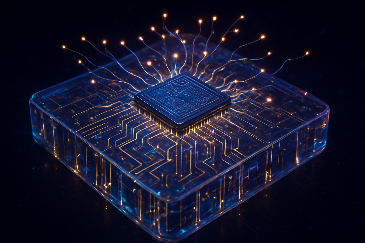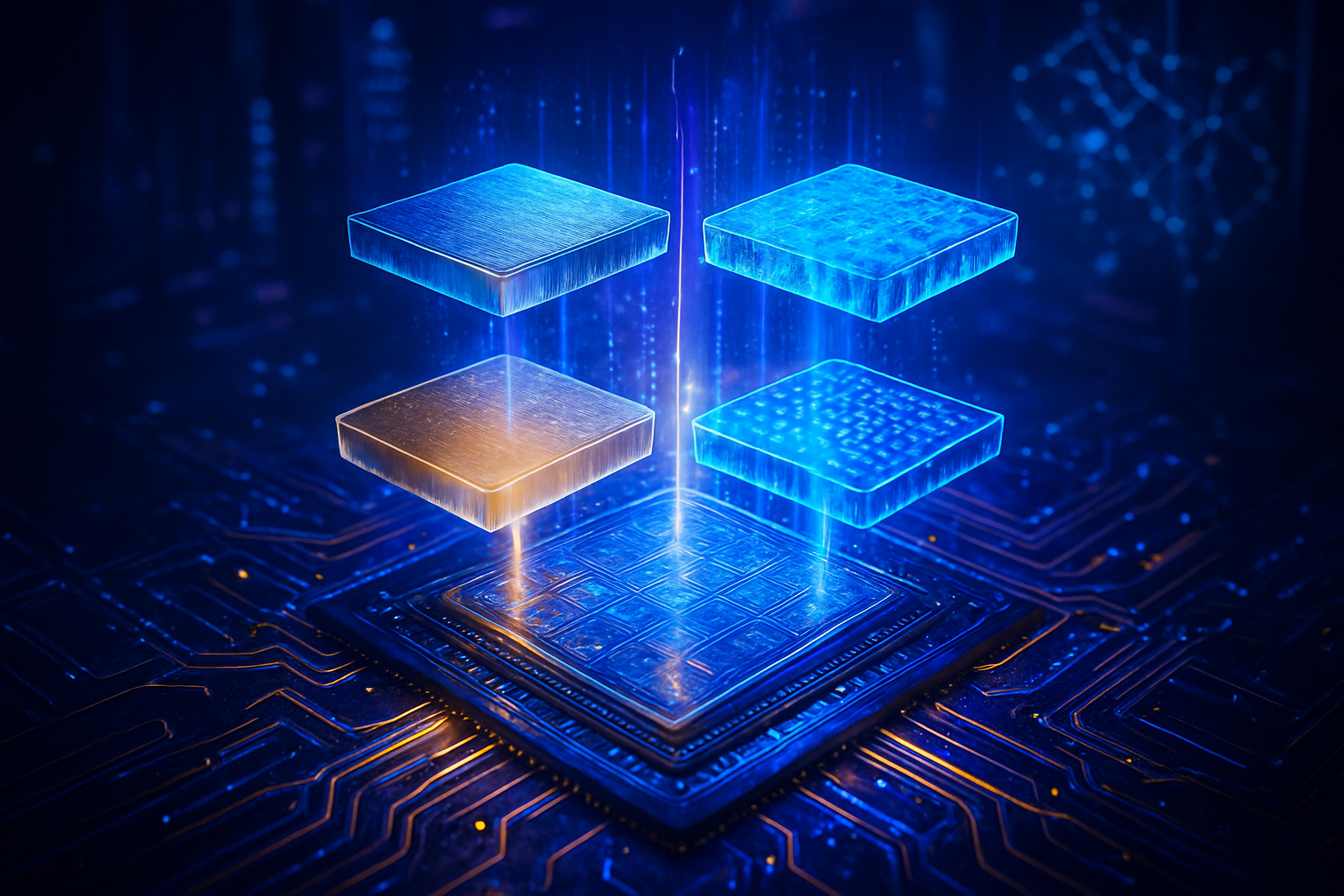
The semiconductor industry has reached a historic inflection point with the full commercial maturity of the Universal Chiplet Interconnect Express (UCIe) 3.0 standard. Officially released in August 2025, this "PCIe for chiplets" has fundamentally transformed how the world’s most powerful processors are built. By providing a standardized, high-speed communication protocol for internal chip components, UCIe 3.0 has effectively ended the era of the "monolithic" processor—where a single company designed and manufactured every square millimeter of a chip’s surface.
This development is not merely a technical upgrade; it is a geopolitical and economic shift. For the first time, the industry has a reliable "lingua franca" that allows for true cross-vendor interoperability. In the high-stakes world of artificial intelligence, this means a single "System-in-Package" (SiP) can now house a compute tile from Intel Corp. (NASDAQ: INTC), a specialized AI accelerator from NVIDIA (NASDAQ: NVDA), and high-bandwidth memory from Samsung Electronics (KRX: 005930). This modular approach, often described as "Silicon Lego," is slashing development costs by an estimated 40% and accelerating the pace of AI innovation to unprecedented levels.
Technical Mastery: Doubling Speed and Extending Reach
The UCIe 3.0 specification represents a massive leap over its predecessors, specifically targeting the extreme bandwidth requirements of 2026-era AI clusters. While UCIe 1.1 and 2.0 topped out at 32 GT/s, the 3.0 standard pushes data rates to a staggering 64 GT/s. This doubling of performance is critical for eliminating the "XPU-to-memory" bottleneck that has plagued large language model (LLM) training. Beyond raw speed, the standard introduces a "Star Topology Sideband," which replaces older management structures with a central "director" chiplet capable of managing multiple disparate tiles with near-zero latency.
One of the most significant technical breakthroughs in UCIe 3.0 is the introduction of "Runtime Recalibration." In previous iterations, a chiplet link would often require a system reboot to adjust for signal drift or power fluctuations. The 3.0 standard allows these links to dynamically adjust power and performance on the fly, a feature essential for the 24/7 uptime required by hyperscale data centers. Furthermore, the "Sideband Reach" has been extended from a mere 25mm to 100mm, allowing for much larger and more complex multi-die packages that can span the entire surface of a server-grade substrate.
The industry response has been swift. Major electronic design automation (EDA) providers like Synopsys (NASDAQ: SNPS) and Cadence Design Systems (NASDAQ: CDNS) have already delivered silicon-proven IP for the 3.0 standard. These tools allow chip designers to "drag and drop" UCIe-compliant interfaces into their designs, ensuring that a custom-built NPU from a startup will communicate seamlessly with a standardized I/O die from a major foundry. This differs from previous proprietary approaches, such as NVIDIA’s NVLink or AMD’s Infinity Fabric, which, while powerful, often acted as "walled gardens" that locked customers into a single vendor's ecosystem.
The New Competitive Chessboard: Foundries and Alliances
The impact of UCIe 3.0 on the corporate landscape is profound, creating both new alliances and intensified rivalries. Intel has been an aggressive proponent of the standard, having donated the original specification to the industry. By early 2025, Intel leveraged its "Systems Foundry" model to launch the Granite Rapids-D Xeon 6 SoC, one of the first high-volume products to use UCIe for modular edge computing. Intel’s strategy is clear: by championing an open standard, they hope to lure fabless companies away from proprietary ecosystems and into their own Foveros packaging facilities.
NVIDIA, long the king of proprietary interconnects, has made a strategic pivot in late 2025. While it continues to use NVLink for its highest-end GPU-to-GPU clusters, it has begun releasing "UCIe-ready" silicon bridges. This move allows third-party manufacturers to build custom security enclaves or specialized accelerators that can plug directly into NVIDIA’s Rubin architecture. This "platformization" of the GPU ensures that NVIDIA remains at the center of the AI universe while benefiting from the specialized innovations of smaller chiplet designers.
Meanwhile, the foundry landscape is witnessing a seismic shift. Samsung Electronics and Intel have reportedly explored a "Foundry Alliance" to challenge the dominance of Taiwan Semiconductor Manufacturing Co. (NYSE: TSM). By standardizing on UCIe 3.0, Samsung and Intel aim to create a viable "second source" for customers who are currently dependent on TSMC’s proprietary CoWoS (Chip on Wafer on Substrate) packaging. TSMC, for its part, continues to lead in sheer volume and yield, but the rise of a standardized "Chiplet Store" threatens its ability to capture the entire value chain of a high-end AI processor.
Wider Significance: Security, Thermals, and the Global Supply Chain
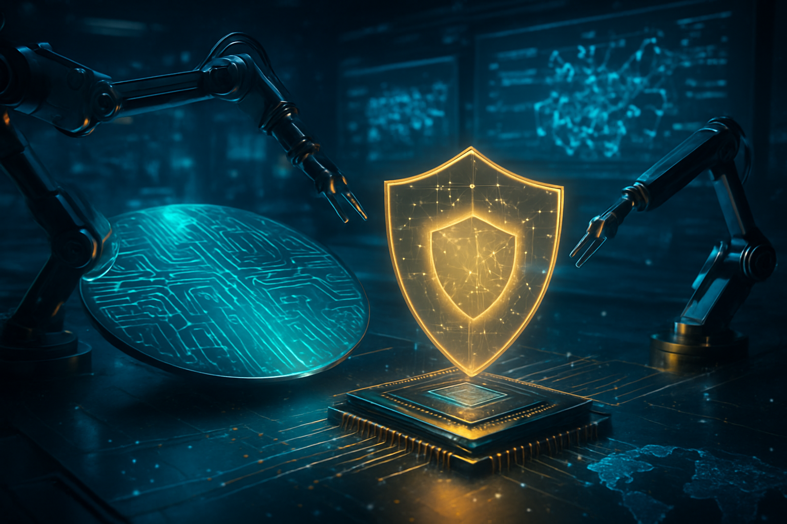
Beyond the balance sheets, UCIe 3.0 addresses the broader evolution of the AI landscape. As AI models become more specialized, the need for "heterogeneous integration"—combining different types of silicon optimized for different tasks—has become a necessity. However, this shift brings new concerns, most notably in the realm of security. With a single package now containing silicon from multiple vendors across different countries, the risk of a "Trojan horse" chiplet has become a major talking point in defense and enterprise circles. To combat this, UCIe 3.0 introduces a standardized "Design for Excellence" (DFx) architecture, enabling hardware-level authentication and isolation between chiplets of varying trust levels.
Thermal management remains the "white whale" of the chiplet era. As UCIe 3.0 enables 3D logic-on-logic stacking with hybrid bonding, the density of transistors has reached a point where traditional air cooling is no longer sufficient. Vertical stacks can create concentrated "hot spots" where a lower die can effectively overheat the components above it. This has spurred a massive industry push toward liquid cooling and in-package microfluidic channels. The shift is also driving interest in glass substrates, which offer superior thermal stability compared to traditional organic materials.
This transition also has significant implications for the global semiconductor supply chain. By disaggregating the chip, companies can now source different components from different regions based on cost or specialized expertise. This "de-risks" the supply chain to some extent, as a shortage in one specific type of compute tile no longer halts the production of an entire monolithic processor. It also allows smaller startups to enter the market by designing a single, high-performance chiplet rather than having to design and fund an entire, multi-billion-dollar SoC.
The Road Ahead: 2026 and the Era of the Custom Superchip
Looking toward 2026, the industry expects the first wave of truly "mix-and-match" commercial products to hit the market. Experts predict that the next generation of AI "Superchips" will not be sold as fixed products, but rather as customizable assemblies. A cloud provider like Amazon (NASDAQ: AMZN) or Microsoft (NASDAQ: MSFT) could theoretically specify a package containing their own custom-designed AI inferencing chiplets, paired with Intel's latest CPU tiles and Samsung’s next-generation HBM4 memory, all stitched together in a single UCIe 3.0-compliant package.
The long-term challenge will be the software stack. While UCIe 3.0 handles the physical and link layers of communication, the industry still lacks a unified software framework for managing a "Frankenstein" chip composed of silicon from five different vendors. Developing these standardized drivers and orchestration layers will be the primary focus of the UCIe Consortium throughout 2026. Furthermore, as the industry moves toward "Optical I/O"—using light instead of electricity to move data between chiplets—UCIe 3.0's flexibility will be tested as it integrates with photonic integrated circuits (PICs).
A New Chapter in Computing History
The maturation of UCIe 3.0 marks the end of the "one-size-fits-all" era of semiconductor design. It is a development that ranks alongside the invention of the integrated circuit and the rise of the PC in its potential to reshape the technological landscape. By lowering the barrier to entry for custom silicon and enabling a modular marketplace for compute, UCIe 3.0 has democratized the ability to build world-class AI hardware.
In the coming months, watch for the first major "inter-vendor" tape-outs, where components from rivals like Intel and NVIDIA are physically combined for the first time. The success of these early prototypes will determine how quickly the industry moves toward a future where "the chip" is no longer a single piece of silicon, but a sophisticated, collaborative ecosystem contained within a few square centimeters of packaging.
This content is intended for informational purposes only and represents analysis of current AI developments.
TokenRing AI delivers enterprise-grade solutions for multi-agent AI workflow orchestration, AI-powered development tools, and seamless remote collaboration platforms.
For more information, visit https://www.tokenring.ai/.