As the artificial intelligence revolution pushes semiconductor design to its physical limits, the industry is reaching a consensus: organic materials can no longer keep up. In a landmark shift for high-performance computing, the world’s leading chipmakers are pivoting toward glass substrates—a transition that promises to redefine the boundaries of chiplet architecture, thermal management, and interconnect density.
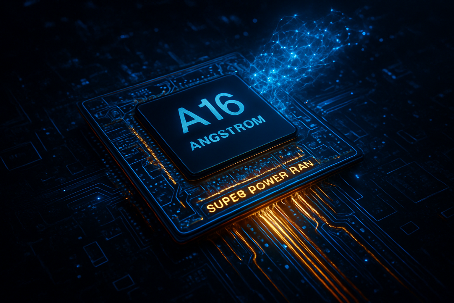
This development marks the end of a decades-long reliance on organic resin-based substrates. As AI models demand trillion-transistor packages and power envelopes exceeding 1,000 watts, the structural and thermal limitations of traditional materials have become a bottleneck. By adopting glass, giants like Intel and Innolux are not just changing a material; they are enabling a new era of "super-chips" that can handle the massive data throughput required for the next generation of generative AI.
The Technical Frontier: Through-Glass Vias and Thermal Superiority
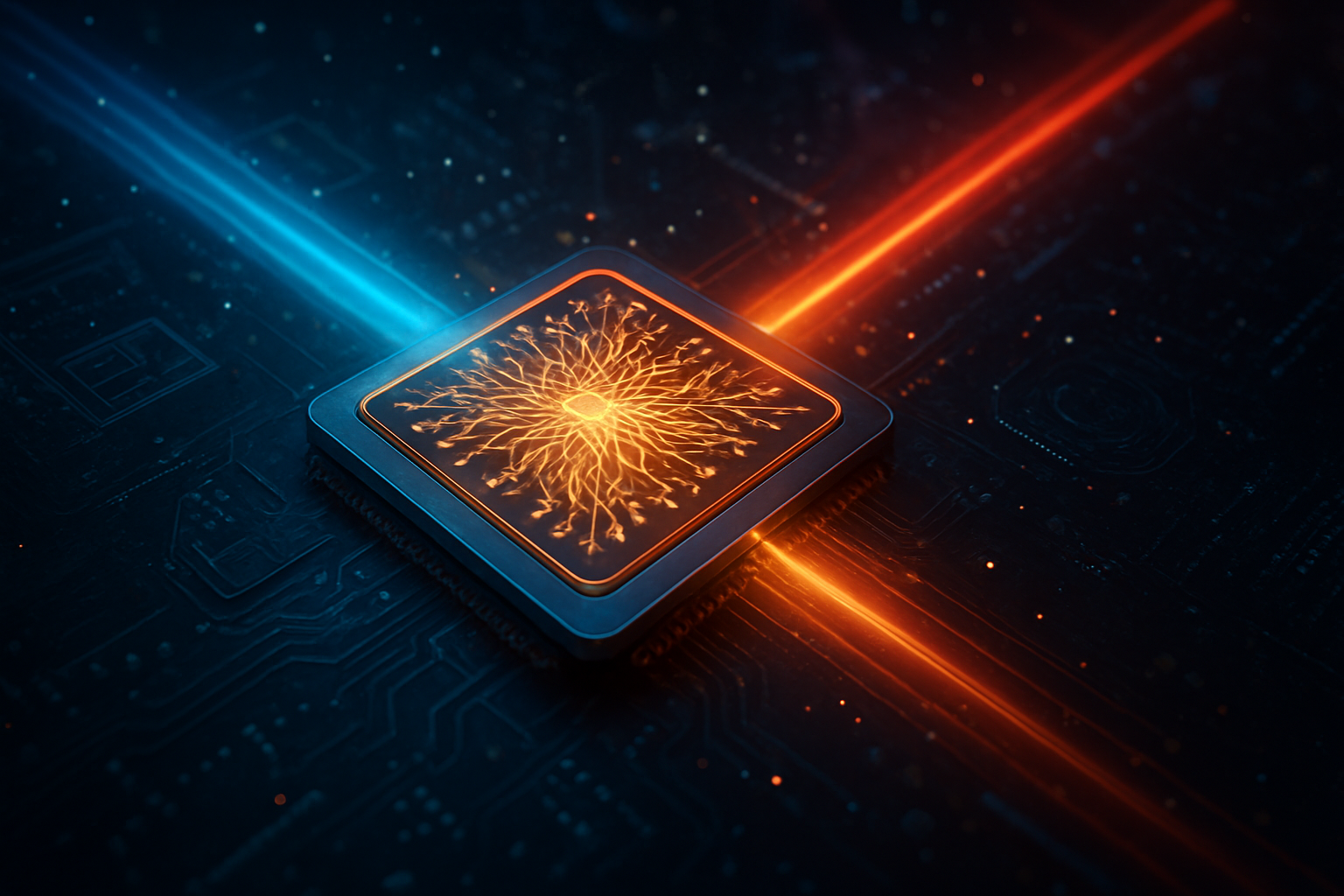
The core of this transition lies in the superior physical properties of glass compared to traditional organic resins like Ajinomoto Build-up Film (ABF). As of late 2025, the industry has mastered Through-Glass Via (TGV) technology, which allows for vertical electrical connections to be etched directly through the glass panel. Unlike organic substrates, which are prone to warping under the intense heat of AI workloads, glass boasts a Coefficient of Thermal Expansion (CTE) that closely matches silicon. This alignment ensures that as a chip heats up, the substrate and the silicon die expand at nearly the same rate, preventing the microscopic copper interconnects between them from cracking or deforming.
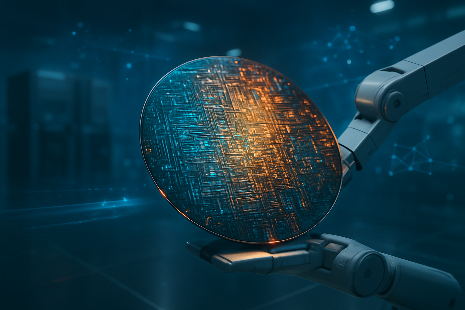
Technically, the shift is staggering. Glass substrates offer a surface flatness of less than 1.0 micrometer, a five-to-tenfold improvement over organic alternatives. This extreme flatness allows for much finer lithography, enabling a 10x increase in interconnect density. Current pilot lines from Intel (NASDAQ: INTC) are demonstrating TGV pitches of less than 100 micrometers, supporting die-to-die bump pitches that were previously impossible. Furthermore, glass provides a 67% reduction in signal loss, a critical factor as AI chips transition to ultra-high-frequency data transfers and eventually, co-packaged optics.
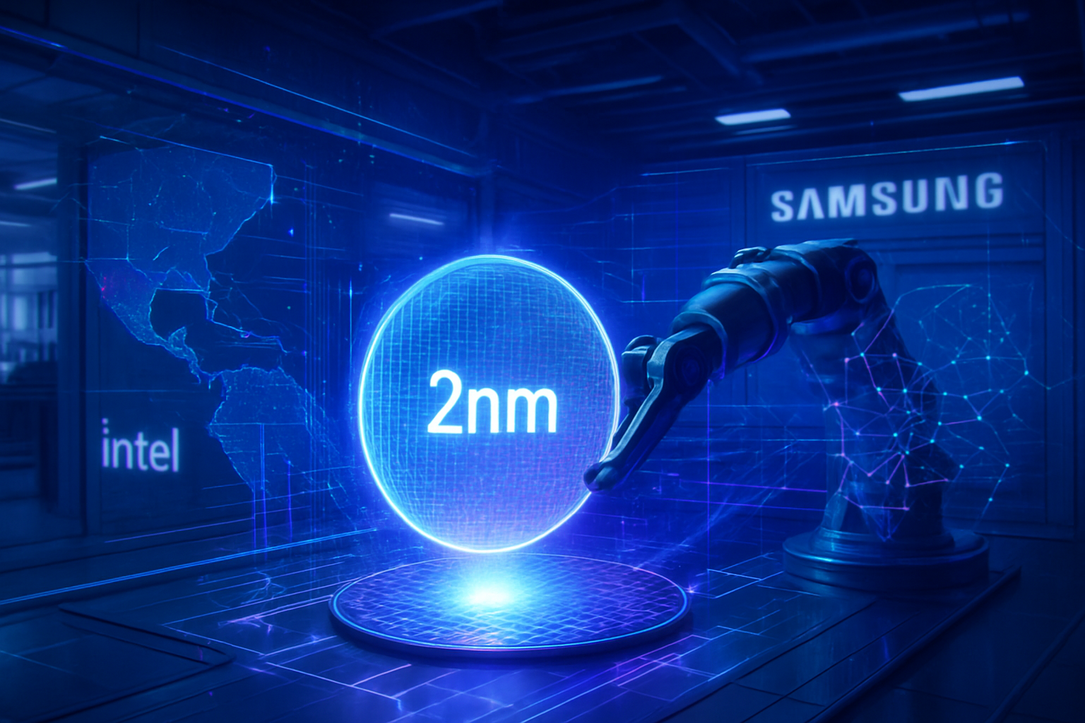
Initial reactions from the semiconductor research community have been overwhelmingly positive, though tempered by the reality of manufacturing yields. Experts note that while glass is more brittle and difficult to handle than organic materials, the "thermal wall" hit by current AI hardware makes the transition inevitable. The ability of glass to remain stable at temperatures up to 400°C—well beyond the 150°C limit where organic resins begin to fail—is being hailed as the "missing link" for the 2nm and 1.4nm process nodes.
Strategic Maneuvers: A New Battlefield for Chip Giants
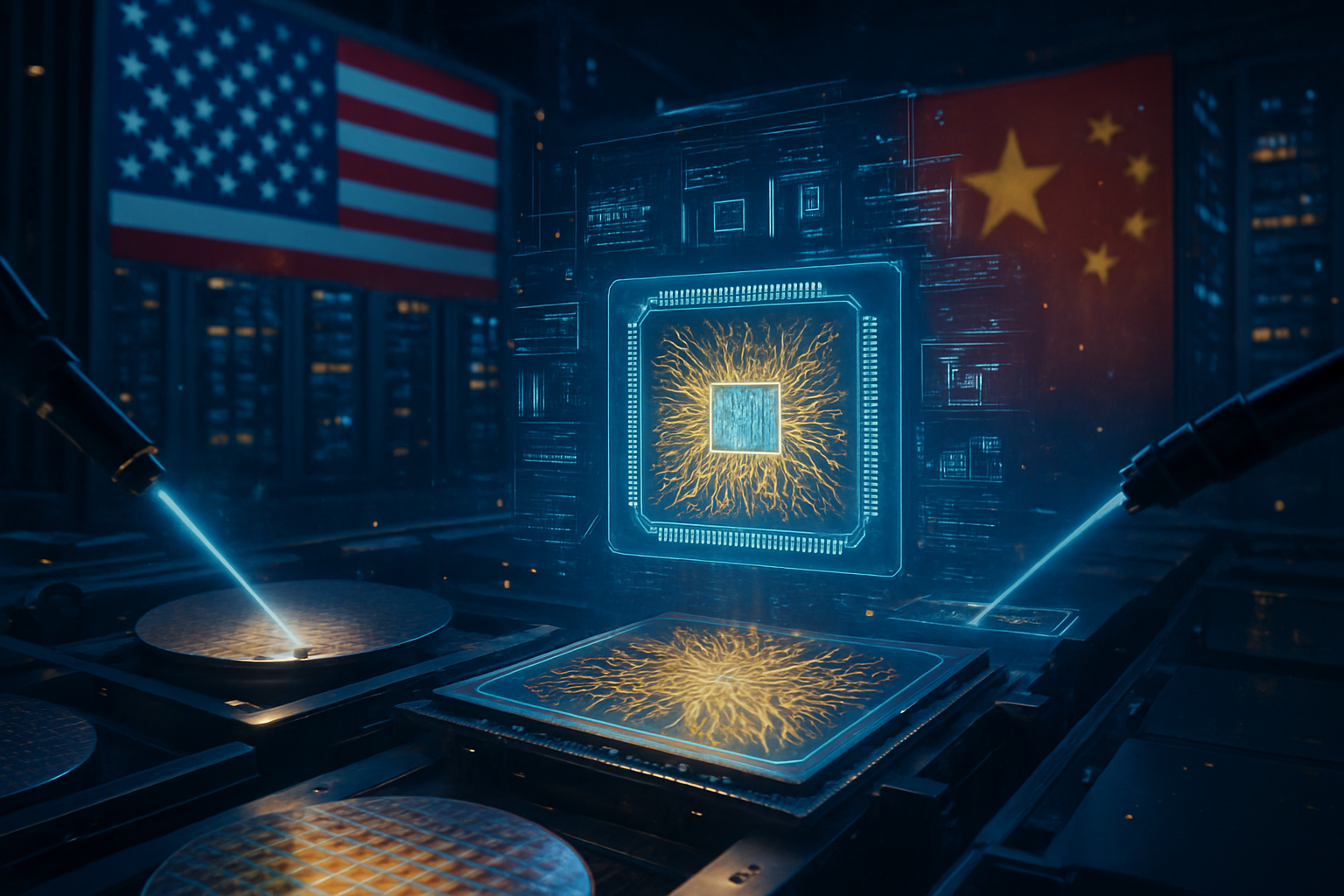
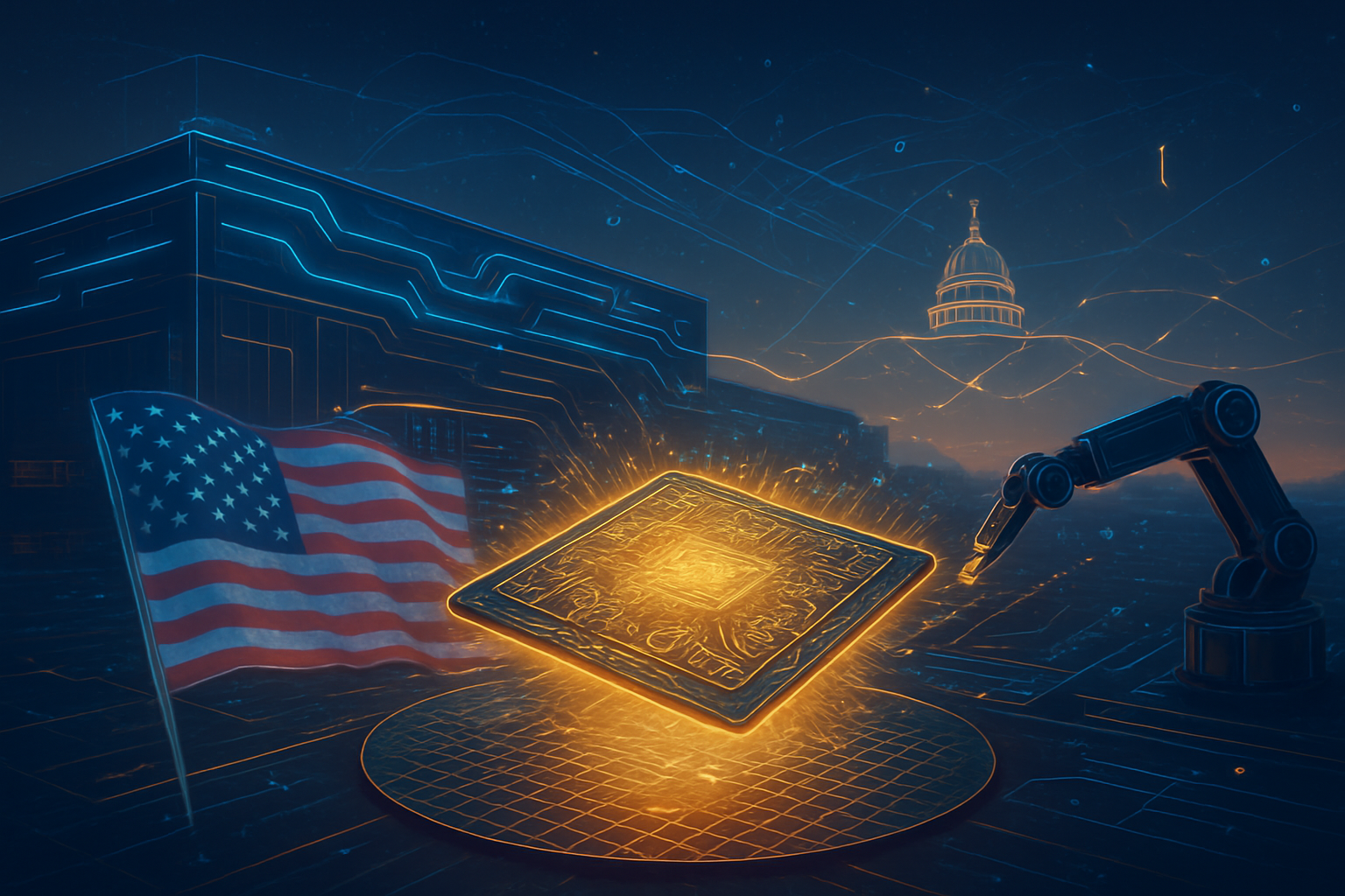
The pivot to glass has ignited a high-stakes arms race among the world’s most powerful technology firms. Intel (NASDAQ: INTC) has taken an early lead, investing over $1 billion into its glass substrate R&D facility in Arizona. By late 2025, Intel has confirmed its roadmap is on track for mass production in 2026, positioning itself to be the primary provider for high-end AI accelerators that require massive, multi-die "System-in-Package" (SiP) designs. This move is a strategic play to regain its manufacturing edge over rivals by offering packaging capabilities that others cannot yet match at scale.
However, the competition is fierce. Samsung (KRX: 005930) has accelerated its own glass substrate program through its subsidiary Samsung Electro-Mechanics, already providing prototype samples to major AI chip designers like AMD (NASDAQ: AMD) and Broadcom (NASDAQ: AVGO). Meanwhile, Innolux (TPE: 3481) has leveraged its expertise in display technology to pivot into Fan-Out Panel-Level Packaging (FOPLP), operating massive 700x700mm panels that offer significant economies of scale. Even the world’s largest foundry, TSMC (NYSE: TSM), has introduced its own glass-based variant, CoPoS (Chip-on-Panel-on-Substrate), to support the next generation of Nvidia architectures.
The market implications are profound. Startups and established AI labs alike will soon have access to hardware that is 15–30% more power-efficient simply due to the packaging shift. This creates a strategic advantage for companies like Amazon (NASDAQ: AMZN), which is reportedly working with the SKC and Applied Materials (NASDAQ: AMAT) joint venture, Absolics, to secure glass substrate capacity for its custom AWS AI chips. Those who successfully integrate glass substrates early will likely lead the next wave of AI performance benchmarks.
Scaling Laws and the Broader AI Landscape
The shift to glass substrates is more than a manufacturing upgrade; it is a necessary evolution to maintain the trajectory of AI scaling laws. As researchers push for larger models with more parameters, the physical size of the AI processor must grow. Traditional organic substrates cannot support the structural rigidity required for the "monster" packages—some exceeding 120x120mm—that are becoming the standard for AI data centers. Glass provides the stiffness and stability to house dozens of chiplets and High Bandwidth Memory (HBM) stacks on a single substrate without the risk of structural failure.
This transition also addresses the growing concern over energy consumption in AI. By reducing electrical impedance and improving signal integrity, glass substrates allow for lower voltage operation, which is vital for sustainable AI growth. However, the pivot is not without its risks. The fragility of glass during the manufacturing process remains a significant hurdle for yields, and the industry must develop entirely new supply chains for high-purity glass panels. Comparisons are already being made to the industry's transition from 200mm to 300mm wafers—a painful but necessary step that unlocked a new decade of growth.
Furthermore, glass substrates are seen as the gateway to Co-Packaged Optics (CPO). Because glass is inherently compatible with optical signals, it allows for the integration of silicon photonics directly into the chip package. This will eventually enable AI chips to communicate via light (photons) rather than electricity (electrons), effectively shattering the current I/O bottlenecks that limit distributed AI training clusters.
The Road Ahead: 2026 and Beyond
Looking forward, the next 12 to 18 months will be defined by the "yield race." While pilot lines are operational in late 2025, the challenge remains in scaling these processes to millions of units. Experts predict that the first commercial AI products featuring glass substrates will hit the market in late 2026, likely appearing in high-end server GPUs and custom ASICs for hyperscalers. These initial applications will focus on the most demanding AI workloads where performance and thermal stability justify the higher cost of glass.
In the long term, we expect glass substrates to trickle down from high-end AI servers to consumer-grade hardware. As the technology matures, it could enable thinner, more powerful laptops and mobile devices with integrated AI capabilities that were previously restricted by thermal constraints. The primary challenge will be the development of standardized TGV processes and the maturation of the glass-handling ecosystem to drive down costs.
A Milestone in Semiconductor History
The industry’s pivot to glass substrates represents one of the most significant packaging breakthroughs in the history of the semiconductor industry. It is a clear signal that the "More than Moore" era has arrived, where gains in performance are driven as much by how chips are packaged and connected as by the transistors themselves. By overcoming the thermal and physical limitations of organic materials, glass substrates provide a new foundation for the trillion-transistor era.
As we move into 2026, the success of this transition will be a key indicator of which semiconductor giants will dominate the AI landscape for the next decade. For now, the focus remains on perfecting the delicate art of Through-Glass Via manufacturing and preparing the global supply chain for a world where glass, not resin, holds the future of intelligence.
This content is intended for informational purposes only and represents analysis of current AI developments.
TokenRing AI delivers enterprise-grade solutions for multi-agent AI workflow orchestration, AI-powered development tools, and seamless remote collaboration platforms.
For more information, visit https://www.tokenring.ai/.