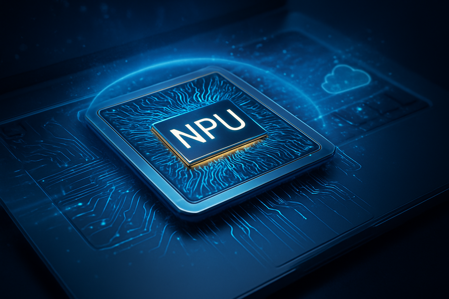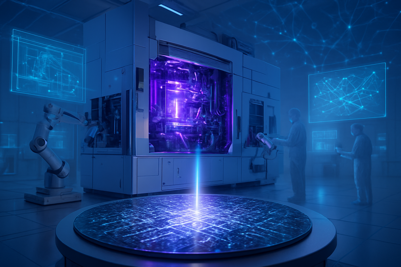
As of late 2025, the semiconductor industry has reached a historic inflection point, driven by the successful transition of High-Numerical Aperture (High-NA) Extreme Ultraviolet (EUV) lithography from experimental labs to the factory floor. ASML (NASDAQ: ASML), the world’s sole provider of the machinery required to print the world’s most advanced chips, has officially entered the high-volume manufacturing (HVM) phase for its next-generation systems. This milestone marks the beginning of the sub-2nm era, providing the essential infrastructure for the next decade of artificial intelligence, high-performance computing, and mobile technology.
The immediate significance of this development cannot be overstated. With the shipment of the Twinscan EXE:5200B to major foundries, the industry has solved the "stitching" and throughput challenges that once threatened to stall Moore’s Law. For ASML, the successful ramp of these multi-hundred-million-dollar machines is the primary engine behind its projected 2030 revenue targets of up to €60 billion. As logic and DRAM manufacturers race to integrate these tools, the gap between those who can afford the "bleeding edge" and those who cannot has never been wider.
Breaking the Sub-2nm Barrier: The Technical Triumph of High-NA
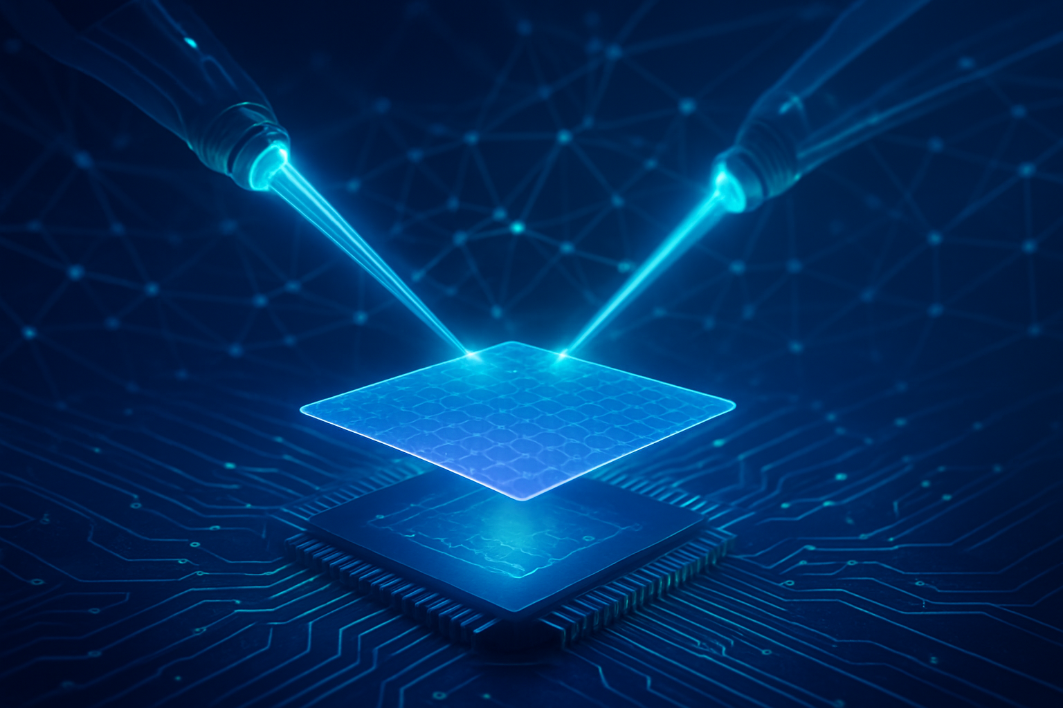
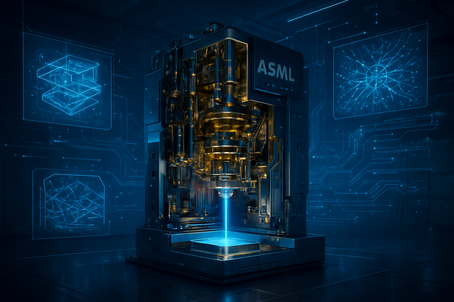
The technical centerpiece of ASML’s 2025 success is the EXE:5200B, a machine that represents the pinnacle of human engineering. Unlike standard EUV tools, which use a 0.33 Numerical Aperture (NA) lens, High-NA systems utilize a 0.55 NA anamorphic lens system. This allows for a significantly higher resolution, enabling chipmakers to print features as small as 8nm—a requirement for the 1.4nm (A14) and 1nm nodes. By late 2025, ASML has successfully boosted the throughput of these systems to 175–200 wafers per hour (wph), matching the productivity of previous generations while drastically reducing the need for "multi-patterning."
One of the most significant technical hurdles overcome this year was "reticle stitching." Because High-NA lenses are anamorphic (magnifying differently in the X and Y directions), the field size is halved compared to standard EUV. This required engineers to "stitch" two halves of a chip design together with nanometer precision. Reports from IMEC and Intel (NASDAQ: INTC) in mid-2025 confirmed that this process has stabilized, allowing for the production of massive AI accelerators that exceed traditional size limits. Furthermore, the industry has begun transitioning to Metal Oxide Resists (MOR), which are thinner and more sensitive than traditional chemically amplified resists, allowing the High-NA light to be captured more effectively.
Initial reactions from the research community have been overwhelmingly positive, with experts noting that High-NA reduces the number of process steps by over 40 on critical layers. This reduction in complexity is vital for yield management at the 1.4nm node. While the sheer cost of the machines—estimated at over $380 million each—initially caused hesitation, the data from 2025 pilot lines has proven that the reduction in mask sets and processing time makes High-NA a cost-effective solution for the highest-volume, highest-performance chips.
The Foundry Arms Race: Intel, TSMC, and Samsung Diverge
The adoption of High-NA has created a strategic divide among the "Big Three" chipmakers. Intel has emerged as the most aggressive pioneer, having fully installed two production-grade EXE:5200 units at its Oregon facility by late 2025. Intel is betting its entire "Intel 14A" roadmap on being the first to market with High-NA, aiming to reclaim the crown of process leadership from TSMC (NYSE: TSM). For Intel, the strategic advantage lies in early mastery of the tool’s quirks, potentially allowing them to offer 1.4nm capacity to external foundry customers before their rivals.
TSMC, conversely, has maintained a pragmatic stance for much of 2025, focusing on its N2 and A16 nodes using standard EUV with multi-patterning. However, the tide shifted in late 2025 when reports surfaced that TSMC had placed significant orders for High-NA machines to support its A14P node, expected to ramp in 2027-2028. This move signals that even the most cost-conscious foundry leader recognizes that standard EUV cannot scale indefinitely. Samsung (KRX: 005930) also took delivery of its first production High-NA unit in Q4 2025, intending to use the technology for its SF1.4 node to close the performance gap in the mobile and AI markets.
The implications for the broader market are profound. Companies like NVIDIA (NASDAQ: NVDA) and Apple (NASDAQ: AAPL) are now forced to navigate this fragmented landscape, deciding whether to stick with TSMC’s proven 0.33 NA methods or pivot to Intel’s High-NA-first approach for their next-generation AI GPUs and silicon. This competition is driving a "supercycle" for ASML, as every major player is forced to buy the most expensive equipment just to stay in the race, further cementing ASML’s monopoly at the top of the supply chain.
Beyond Logic: EUV’s Critical Role in DRAM and Global Trends
While logic manufacturing often grabs the headlines, 2025 has been the year EUV became indispensable for memory. The mass production of "1c" (12nm-class) DRAM is now in full swing, with SK Hynix (KRX: 000660) leading the charge by utilizing five to six EUV layers for its HBM4 (High Bandwidth Memory) products. Even Micron (NASDAQ: MU), which was famously the last major holdout for EUV technology, has successfully ramped its 1-gamma node using EUV at its Hiroshima plant this year. The integration of EUV in DRAM is critical for ASML’s long-term margins, as memory manufacturers typically purchase tools in higher volumes than logic foundries.
This shift fits into a broader global trend: the AI Supercycle. The explosion in demand for generative AI has created a bottomless appetite for high-density memory and high-performance logic, both of which now require EUV. However, this growth is occurring against a backdrop of geopolitical complexity. ASML has reported that while demand from China has normalized—dropping to roughly 20% of revenue from nearly 50% in 2024 due to export restrictions—the global demand for advanced tools has more than compensated. ASML’s gross margin targets of 56% to 60% by 2030 are predicated on this shift toward higher-value High-NA systems and the expansion of EUV into the memory sector.
Comparisons to previous milestones, such as the initial move from DUV to EUV in 2018, suggest that we are entering a "harvesting" phase. The foundational science is settled, and the focus has shifted to industrialization and yield optimization. The potential concern remains the "cost wall"—the risk that only a handful of companies can afford to design chips at the 1.4nm level, potentially centralizing the AI industry even further into the hands of a few tech giants.
The Roadmap to 2030: From High-NA to Hyper-NA
Looking ahead, ASML is already laying the groundwork for the next decade with "Hyper-NA" lithography. As High-NA carries the industry through the 1.4nm and 1nm eras, the subsequent generation of transistors—likely based on Complementary FET (CFET) architectures—will require even higher resolution. ASML’s roadmap for the HXE series targets a 0.75 NA, which would be the most significant jump in optical capability in the company's history. Pilot systems for Hyper-NA are currently projected for introduction around 2030.
The challenges for Hyper-NA are daunting. At 0.75 NA, the depth of focus becomes extremely shallow, and light polarization effects can degrade image contrast. ASML is currently researching specialized polarization filters and even more advanced photoresist materials to combat these physics-based limitations. Experts predict that the move to Hyper-NA will be as difficult as the original transition to EUV, requiring a complete overhaul of the mask and pellicle ecosystem. However, if successful, it will extend the life of silicon-based computing well into the 2030s.
In the near term, the industry will focus on the "A14" ramp. We expect to see the first silicon samples from Intel’s High-NA lines by mid-2026, which will be the ultimate test of whether the technology can deliver on its promise of superior power, performance, and area (PPA). If Intel succeeds in hitting its yield targets, it could trigger a massive wave of "FOMO" (fear of missing out) among other chipmakers, leading to an even faster adoption rate for ASML’s most advanced tools.
Conclusion: The Indispensable Backbone of AI
The status of ASML and EUV lithography at the end of 2025 confirms one undeniable truth: the future of artificial intelligence is physically etched by a single company in Veldhoven. The successful deployment of High-NA lithography has effectively moved the goalposts for Moore’s Law, ensuring that the roadmap to sub-2nm chips is not just a theoretical possibility but a manufacturing reality. ASML’s ability to maintain its technological lead while expanding its margins through logic and DRAM adoption has solidified its position as the most critical node in the global technology supply chain.
As we move into 2026, the industry will be watching for the first "High-NA chips" to enter the market. The success of these products will determine the pace of the next decade of computing. For now, ASML has proven that it can meet the moment, providing the tools necessary to build the increasingly complex brains of the AI era. The "High-NA Era" has officially arrived, and with it, a new chapter in the history of human innovation.
This content is intended for informational purposes only and represents analysis of current AI developments.
TokenRing AI delivers enterprise-grade solutions for multi-agent AI workflow orchestration, AI-powered development tools, and seamless remote collaboration platforms.
For more information, visit https://www.tokenring.ai/.