Tag: Intel

  • Intel Foundry Secures Landmark Microsoft Maia 2 Deal on 18A Node: A New Dawn for AI Silicon Manufacturing

    Intel Foundry Secures Landmark Microsoft Maia 2 Deal on 18A Node: A New Dawn for AI Silicon Manufacturing

    In a monumental shift poised to redefine the AI semiconductor landscape, Intel Foundry has officially secured a pivotal contract to manufacture Microsoft's (NASDAQ: MSFT) next-generation AI accelerator, Maia 2, utilizing its cutting-edge 18A process node. This announcement, solidifying earlier speculation as of October 17, 2025, marks a significant validation of Intel's (NASDAQ: INTC) ambitious IDM 2.0 strategy and a strategic move by Microsoft to diversify its critical AI supply chain. The multi-billion-dollar deal not only cements Intel's re-emergence as a formidable player in advanced foundry services but also signals a new era of intensified competition and innovation in the race for AI supremacy.

    The collaboration underscores the growing trend among hyperscalers to design custom silicon tailored for their unique AI workloads, moving beyond reliance on off-the-shelf solutions. By entrusting Intel with the fabrication of Maia 2, Microsoft aims to optimize performance, efficiency, and cost for its vast Azure cloud infrastructure, powering the generative AI explosion. For Intel, this contract represents a vital win, demonstrating the technological maturity and competitiveness of its 18A node against established foundry giants and potentially attracting a cascade of new customers to its Foundry Services division.

    Unpacking the Technical Revolution: Maia 2 and the 18A Node

    The Microsoft Maia 2, while specific technical details remain under wraps, is anticipated to be a significant leap forward from its predecessor, Maia 100. The first-generation Maia 100, fabricated on TSMC's (NYSE: TSM) N5 process, boasted an 820 mm² die, 105 billion transistors, and 64 GB of HBM2E memory. Maia 2, leveraging Intel's advanced 18A or 18A-P process, is expected to push these boundaries further, delivering enhanced performance-per-watt metrics crucial for the escalating demands of large-scale AI model training and inference.

    At the heart of this technical breakthrough is Intel's 18A node, a 2-nanometer class process that integrates two groundbreaking innovations. Firstly, RibbonFET, Intel's implementation of a Gate-All-Around (GAA) transistor architecture, replaces traditional FinFETs. This design allows for greater scaling, reduced power leakage, and improved performance at lower voltages, directly addressing the power and efficiency challenges inherent in AI chip design. Secondly, PowerVia, a backside power delivery network, separates power routing from signal routing, significantly reducing signal interference, enhancing transistor density, and boosting overall performance.

    Compared to Intel's prior Intel 3 node, 18A promises over a 15% iso-power performance gain and up to 38% power savings at the same clock speeds below 0.65V, alongside a substantial density improvement of up to 39%. The enhanced 18A-P variant further refines these technologies, incorporating second-generation RibbonFET and PowerVia, alongside optimized components to reduce leakage and improve performance-per-watt. This advanced manufacturing capability provides Microsoft with the crucial technological edge needed to design highly efficient and powerful AI accelerators for its demanding data center environments, distinguishing Maia 2 from previous approaches and existing technologies. The initial reaction from the AI research community and industry experts has been overwhelmingly positive, viewing this as a strong signal of Intel's foundry resurgence and Microsoft's commitment to custom AI silicon.

    Reshaping the AI Industry: Competitive Dynamics and Strategic Advantages

    This landmark deal will send ripples across the entire AI ecosystem, profoundly impacting AI companies, tech giants, and startups alike. Intel stands to benefit immensely, with the Microsoft contract serving as a powerful validation of its IDM 2.0 strategy and a clear signal that its advanced nodes are competitive. This could attract other major hyperscalers and fabless AI chip designers, accelerating the ramp-up of its foundry business and providing a much-needed financial boost, with the deal's lifetime value reportedly exceeding $15 billion.

    For Microsoft, the strategic advantages are multifaceted. Securing a reliable, geographically diverse supply chain for its critical AI hardware mitigates geopolitical risks and reduces reliance on a single foundry. This vertical integration allows Microsoft to co-design its hardware and software more closely, optimizing Maia 2 for its specific Azure AI workloads, leading to superior performance, lower latency, and potentially significant cost efficiencies. This move further strengthens Microsoft's market positioning in the fiercely competitive cloud AI space, enabling it to offer differentiated services and capabilities to its customers.

    The competitive implications for major AI labs and tech companies are substantial. While TSMC (NYSE: TSM) has long dominated the advanced foundry market, Intel's successful entry with a marquee customer like Microsoft intensifies competition, potentially leading to faster innovation cycles and more favorable pricing for future AI chip designs. This also highlights a broader trend: the increasing willingness of tech giants to invest in custom silicon, which could disrupt existing products and services from traditional GPU providers and accelerate the shift towards specialized AI hardware. Startups in the AI chip design space may find more foundry options available, fostering a more dynamic and diverse hardware ecosystem.

    Broader Implications for the AI Landscape and Future Trends

    The Intel-Microsoft partnership is more than just a business deal; it's a significant indicator of the evolving AI landscape. It reinforces the industry's pivot towards custom silicon and diversified supply chains as critical components for scaling AI infrastructure. The geopolitical climate, characterized by increasing concerns over semiconductor supply chain resilience, makes this U.S.-based manufacturing collaboration particularly impactful, contributing to a more robust and geographically balanced global tech ecosystem.

    This development fits into broader AI trends that emphasize efficiency, specialization, and vertical integration. As AI models grow exponentially in size and complexity, generic hardware solutions become less optimal. Companies like Microsoft are responding by designing chips that are hyper-optimized for their specific software stacks and data center environments. This strategic alignment can unlock unprecedented levels of performance and energy efficiency, which are crucial for sustainable AI development.

    Potential concerns include the execution risk for Intel, as ramping up a leading-edge process node to high volume and yield consistently is a monumental challenge. However, Intel's recent announcement that its Panther Lake processors, also on 18A, have entered volume production at Fab 52, with broad market availability slated for January 2026, provides a strong signal of their progress. This milestone, coming just eight days before the specific Maia 2 confirmation, demonstrates Intel's commitment and capability. Comparisons to previous AI milestones, such as Google's (NASDAQ: GOOGL) development of its custom Tensor Processing Units (TPUs), highlight the increasing importance of custom hardware in driving AI breakthroughs. This Intel-Microsoft collaboration represents a new frontier in that journey, focusing on open foundry relationships for such advanced custom designs.

    Charting the Course: Future Developments and Expert Predictions

    Looking ahead, the successful fabrication and deployment of Microsoft's Maia 2 on Intel's 18A node are expected to catalyze several near-term and long-term developments. Mass production of Maia 2 is anticipated to commence in 2026, potentially following an earlier reported delay, aligning with Intel's broader 18A ramp-up. This will pave the way for Microsoft to deploy these accelerators across its Azure data centers, significantly boosting its AI compute capabilities and enabling more powerful and efficient AI services for its customers.

    Future applications and use cases on the horizon are vast, ranging from accelerating advanced large language models (LLMs) and multimodal AI to enhancing cognitive services, intelligent automation, and personalized user experiences across Microsoft's product portfolio. The continued evolution of the 18A node, with planned variants like 18A-P for performance optimization and 18A-PT for multi-die architectures and advanced hybrid bonding, suggests a roadmap for even more sophisticated AI chips in the future.

    Challenges that need to be addressed include achieving consistent high yield rates at scale for the 18A node, ensuring seamless integration of Maia 2 into Microsoft's existing hardware and software ecosystem, and navigating the intense competitive landscape where TSMC and Samsung (KRX: 005930) are also pushing their own advanced nodes. Experts predict a continued trend of vertical integration among hyperscalers, with more companies opting for custom silicon and leveraging multiple foundry partners to de-risk their supply chains and optimize for specific workloads. This diversified approach is likely to foster greater innovation and resilience within the AI hardware sector.

    A Pivotal Moment: Comprehensive Wrap-Up and Long-Term Impact

    The Intel Foundry and Microsoft Maia 2 deal on the 18A node represents a truly pivotal moment in the history of AI semiconductor manufacturing. The key takeaways underscore Intel's remarkable comeback as a leading-edge foundry, Microsoft's strategic foresight in securing its AI future through custom silicon and supply chain diversification, and the profound implications for the broader AI industry. This collaboration signifies not just a technical achievement but a strategic realignment that will reshape the competitive dynamics of AI hardware for years to come.

    This development's significance in AI history cannot be overstated. It marks a crucial step towards a more robust, competitive, and geographically diversified semiconductor supply chain, essential for the sustained growth and innovation of artificial intelligence. It also highlights the increasing sophistication and strategic importance of custom AI silicon, solidifying its role as a fundamental enabler for next-generation AI capabilities.

    In the coming weeks and months, the industry will be watching closely for several key indicators: the successful ramp-up of Intel's 18A production, the initial performance benchmarks and deployment of Maia 2 by Microsoft, and the competitive responses from other major foundries and AI chip developers. This partnership is a clear signal that the race for AI supremacy is not just about algorithms and software; it's fundamentally about the underlying hardware and the manufacturing prowess that brings it to life.


    This content is intended for informational purposes only and represents analysis of current AI developments.

    TokenRing AI delivers enterprise-grade solutions for multi-agent AI workflow orchestration, AI-powered development tools, and seamless remote collaboration platforms.
    For more information, visit https://www.tokenring.ai/.

  • The Dawn of Hyper-Specialized AI: New Chip Architectures Redefine Performance and Efficiency

    The Dawn of Hyper-Specialized AI: New Chip Architectures Redefine Performance and Efficiency

    The artificial intelligence landscape is undergoing a profound transformation, driven by a new generation of AI-specific chip architectures that are dramatically enhancing performance and efficiency. As of October 2025, the industry is witnessing a pivotal shift away from reliance on general-purpose GPUs towards highly specialized processors, meticulously engineered to meet the escalating computational demands of advanced AI models, particularly large language models (LLMs) and generative AI. This hardware renaissance promises to unlock unprecedented capabilities, accelerate AI development, and pave the way for more sophisticated and energy-efficient intelligent systems.

    The immediate significance of these advancements is a substantial boost in both AI performance and efficiency across the board. Faster training and inference speeds, coupled with dramatic improvements in energy consumption, are not merely incremental upgrades; they are foundational changes enabling the next wave of AI innovation. By overcoming memory bottlenecks and tailoring silicon to specific AI workloads, these new architectures are making previously resource-intensive AI applications more accessible and sustainable, marking a critical inflection point in the ongoing AI supercycle.

    Unpacking the Engineering Marvels: A Deep Dive into Next-Gen AI Silicon

    The current wave of AI chip innovation is characterized by a multi-pronged approach, with hyperscalers, established GPU giants, and innovative startups pushing the boundaries of what's possible. These advancements showcase a clear trend towards specialization, high-bandwidth memory integration, and groundbreaking new computing paradigms.

    Hyperscale cloud providers are leading the charge with custom silicon designed for their specific workloads. Google's (NASDAQ: GOOGL) unveiling of Ironwood, its seventh-generation Tensor Processing Unit (TPU), stands out. Designed specifically for inference, Ironwood delivers an astounding 42.5 exaflops of performance, representing a nearly 2x improvement in energy efficiency over its predecessors and an almost 30-fold increase in power efficiency compared to the first Cloud TPU from 2018. It boasts an enhanced SparseCore, a massive 192 GB of High Bandwidth Memory (HBM) per chip (6x that of Trillium), and a dramatically improved HBM bandwidth of 7.37 TB/s. These specifications are crucial for accelerating enterprise AI applications and powering complex models like Gemini 2.5.

    Traditional GPU powerhouses are not standing still. Nvidia's (NASDAQ: NVDA) Blackwell architecture, including the B200 and the upcoming Blackwell Ultra (B300-series) expected in late 2025, is in full production. The Blackwell Ultra promises 20 petaflops and a 1.5x performance increase over the original Blackwell, specifically targeting AI reasoning workloads with 288GB of HBM3e memory. Blackwell itself offers a substantial generational leap over its predecessor, Hopper, being up to 2.5 times faster for training and up to 30 times faster for cluster inference, with 25 times better energy efficiency for certain inference tasks. Looking further ahead, Nvidia's Rubin AI platform, slated for mass production in late 2025 and general availability in early 2026, will feature an entirely new architecture, advanced HBM4 memory, and NVLink 6, further solidifying Nvidia's dominant 86% market share in 2025. Not to be outdone, AMD (NASDAQ: AMD) is rapidly advancing its Instinct MI300X and the upcoming MI350 series GPUs. The MI325X accelerator, with 288GB of HBM3E memory, was generally available in Q4 2024, while the MI350 series, expected in 2025, promises up to a 35x increase in AI inference performance. The MI450 Series AI chips are also set for deployment by Oracle Cloud Infrastructure (NYSE: ORCL) starting in Q3 2026. Intel (NASDAQ: INTC), while canceling its Falcon Shores commercial offering, is focusing on a "system-level solution at rack scale" with its successor, Jaguar Shores. For AI inference, Intel unveiled "Crescent Island" at the 2025 OCP Global Summit, a new data center GPU based on the Xe3P architecture, optimized for performance-per-watt, and featuring 160GB of LPDDR5X memory, ideal for "tokens-as-a-service" providers.

    Beyond traditional architectures, emerging computing paradigms are gaining significant traction. In-Memory Computing (IMC) chips, designed to perform computations directly within memory, are dramatically reducing data movement bottlenecks and power consumption. IBM Research (NYSE: IBM) has showcased scalable hardware with 3D analog in-memory architecture for large models and phase-change memory for compact edge-sized models, demonstrating exceptional throughput and energy efficiency for Mixture of Experts (MoE) models. Neuromorphic computing, inspired by the human brain, utilizes specialized hardware chips with interconnected neurons and synapses, offering ultra-low power consumption (up to 1000x reduction) and real-time learning. Intel's Loihi 2 and IBM's TrueNorth are leading this space, alongside startups like BrainChip (Akida Pulsar, July 2025, 500 times lower energy consumption) and Innatera Nanosystems (Pulsar, May 2025). Chinese researchers also unveiled SpikingBrain 1.0 in October 2025, claiming it to be 100 times faster and more energy-efficient than traditional systems. Photonic AI chips, which use light instead of electrons, promise extremely high bandwidth and low power consumption, with Tsinghua University's Taichi chip (April 2024) claiming 1,000 times more energy-efficiency than Nvidia's H100.

    Reshaping the AI Industry: Competitive Implications and Market Dynamics

    These advancements in AI-specific chip architectures are fundamentally reshaping the competitive landscape for AI companies, tech giants, and startups alike. The drive for specialized silicon is creating both new opportunities and significant challenges, influencing strategic advantages and market positioning.

    Hyperscalers like Google, Amazon (NASDAQ: AMZN), and Microsoft (NASDAQ: MSFT), with their deep pockets and immense AI workloads, stand to benefit significantly from their custom silicon efforts. Google's Ironwood TPU, for instance, provides a tailored, highly optimized solution for its internal AI development and Google Cloud customers, offering a distinct competitive edge in performance and cost-efficiency. This vertical integration allows them to fine-tune hardware and software, delivering superior end-to-end solutions.

    For major AI labs and tech companies, the competitive implications are profound. While Nvidia continues to dominate the AI GPU market, the rise of custom silicon from hyperscalers and the aggressive advancements from AMD pose a growing challenge. Companies that can effectively leverage these new, more efficient architectures will gain a significant advantage in model training times, inference costs, and the ability to deploy larger, more complex AI models. The focus on energy efficiency is also becoming a key differentiator, as the operational costs and environmental impact of AI grow exponentially. This could disrupt existing products or services that rely on older, less efficient hardware, pushing companies to rapidly adopt or develop their own specialized solutions.

    Startups specializing in emerging architectures like neuromorphic, photonic, and in-memory computing are poised for explosive growth. Their ability to deliver ultra-low power consumption and unprecedented efficiency for specific AI tasks opens up new markets, particularly at the edge (IoT, robotics, autonomous vehicles) where power budgets are constrained. The AI ASIC market itself is projected to reach $15 billion in 2025, indicating a strong appetite for specialized solutions. Market positioning will increasingly depend on a company's ability to offer not just raw compute power, but also highly optimized, energy-efficient, and domain-specific solutions that address the nuanced requirements of diverse AI applications.

    The Broader AI Landscape: Impacts, Concerns, and Future Trajectories

    The current evolution in AI-specific chip architectures fits squarely into the broader AI landscape as a critical enabler of the ongoing "AI supercycle." These hardware innovations are not merely making existing AI faster; they are fundamentally expanding the horizons of what AI can achieve, paving the way for the next generation of intelligent systems that are more powerful, pervasive, and sustainable.

    The impacts are wide-ranging. Dramatically faster training times mean AI researchers can iterate on models more rapidly, accelerating breakthroughs. Improved inference efficiency allows for the deployment of sophisticated AI in real-time applications, from autonomous vehicles to personalized medical diagnostics, with lower latency and reduced operational costs. The significant strides in energy efficiency, particularly from neuromorphic and in-memory computing, are crucial for addressing the environmental concerns associated with the burgeoning energy demands of large-scale AI. This "hardware renaissance" is comparable to previous AI milestones, such as the advent of GPU acceleration for deep learning, but with an added layer of specialization that promises even greater gains.

    However, this rapid advancement also brings potential concerns. The high development costs associated with designing and manufacturing cutting-edge chips could further concentrate power among a few large corporations. There's also the potential for hardware fragmentation, where a diverse ecosystem of specialized chips might complicate software development and interoperability. Companies and developers will need to invest heavily in adapting their software stacks to leverage the unique capabilities of these new architectures, posing a challenge for smaller players. Furthermore, the increasing complexity of these chips demands specialized talent in chip design, AI engineering, and systems integration, creating a talent gap that needs to be addressed.

    The Road Ahead: Anticipating What Comes Next

    Looking ahead, the trajectory of AI-specific chip architectures points towards continued innovation and further specialization, with profound implications for future AI applications. Near-term developments will see the refinement and wider adoption of current generation technologies. Nvidia's Rubin platform, AMD's MI350/MI450 series, and Intel's Jaguar Shores will continue to push the boundaries of traditional accelerator performance, while HBM4 memory will become standard, enabling even larger and more complex models.

    In the long term, we can expect the maturation and broader commercialization of emerging paradigms like neuromorphic, photonic, and in-memory computing. As these technologies scale and become more accessible, they will unlock entirely new classes of AI applications, particularly in areas requiring ultra-low power, real-time adaptability, and on-device learning. There will also be a greater integration of AI accelerators directly into CPUs, creating more unified and efficient computing platforms.

    Potential applications on the horizon include highly sophisticated multimodal AI systems that can seamlessly understand and generate information across various modalities (text, image, audio, video), truly autonomous systems capable of complex decision-making in dynamic environments, and ubiquitous edge AI that brings intelligent processing closer to the data source. Experts predict a future where AI is not just faster, but also more pervasive, personalized, and environmentally sustainable, driven by these hardware advancements. The challenges, however, will involve scaling manufacturing to meet demand, ensuring interoperability across diverse hardware ecosystems, and developing robust software frameworks that can fully exploit the unique capabilities of each architecture.

    A New Era of AI Computing: The Enduring Impact

    In summary, the latest advancements in AI-specific chip architectures represent a critical inflection point in the history of artificial intelligence. The shift towards hyper-specialized silicon, ranging from hyperscaler custom TPUs to groundbreaking neuromorphic and photonic chips, is fundamentally redefining the performance, efficiency, and capabilities of AI applications. Key takeaways include the dramatic improvements in training and inference speeds, unprecedented energy efficiency gains, and the strategic importance of overcoming memory bottlenecks through innovations like HBM4 and in-memory computing.

    This development's significance in AI history cannot be overstated; it marks a transition from a general-purpose computing era to one where hardware is meticulously crafted for the unique demands of AI. This specialization is not just about making existing AI faster; it's about enabling previously impossible applications and democratizing access to powerful AI by making it more efficient and sustainable. The long-term impact will be a world where AI is seamlessly integrated into every facet of technology and society, from the cloud to the edge, driving innovation across all industries.

    As we move forward, what to watch for in the coming weeks and months includes the commercial success and widespread adoption of these new architectures, the continued evolution of Nvidia, AMD, and Google's next-generation chips, and the critical development of software ecosystems that can fully harness the power of this diverse and rapidly advancing hardware landscape. The race for AI supremacy will increasingly be fought on the silicon frontier.


    This content is intended for informational purposes only and represents analysis of current AI developments.

    TokenRing AI delivers enterprise-grade solutions for multi-agent AI workflow orchestration, AI-powered development tools, and seamless remote collaboration platforms.
    For more information, visit https://www.tokenring.ai/.

  • Semiconductor Stocks Soar Amidst AI Supercycle: A Resilient Tech Market Defies Fluctuations

    Semiconductor Stocks Soar Amidst AI Supercycle: A Resilient Tech Market Defies Fluctuations

    The technology sector is currently experiencing a remarkable surge in optimism, particularly evident in the robust performance of semiconductor stocks. This positive sentiment, observed around October 2025, is largely driven by the burgeoning "AI Supercycle"—an era of immense and insatiable demand for artificial intelligence and high-performance computing (HPC) capabilities. Despite broader market fluctuations and ongoing geopolitical concerns, the semiconductor industry has been propelled to new financial heights, establishing itself as the fundamental building block of a global AI-driven economy.

    This unprecedented demand for advanced silicon is creating a new data center ecosystem and fostering an environment where innovation in chip design and manufacturing is paramount. Leading semiconductor companies are not merely benefiting from this trend; they are actively shaping the future of AI by delivering the foundational hardware that underpins every major AI advancement, from large language models to autonomous systems.

    The Silicon Engine of AI: Unpacking Technical Advancements Driving the Boom

    The current semiconductor boom is underpinned by relentless technical advancements in AI chips, including Graphics Processing Units (GPUs), Application-Specific Integrated Circuits (ASICs), and High Bandwidth Memory (HBM). These innovations are delivering immense computational power and efficiency, essential for the escalating demands of generative AI, large language models (LLMs), and high-performance computing workloads.

    Leading the charge in GPUs, Nvidia (NASDAQ: NVDA) has introduced its H200 (Hopper Architecture), featuring 141 GB of HBM3e memory—a significant leap from the H100's 80 GB—and offering 4.8 TB/s of memory bandwidth. This translates to substantial performance boosts, including up to 4 petaFLOPS of FP8 performance and nearly double the inference performance for LLMs like Llama2 70B compared to its predecessor. Nvidia's upcoming Blackwell architecture (launched in 2025) and Rubin GPU platform (2026) promise even greater transformer acceleration and HBM4 memory integration. AMD (NASDAQ: AMD) is aggressively challenging with its Instinct MI300 series (CDNA 3 Architecture), including the MI300A APU and MI300X accelerator, which boast up to 192 GB of HBM3 memory and 5.3 TB/s bandwidth. The AMD Instinct MI325X and MI355X further push the boundaries with up to 288 GB of HBM3e and 8 TBps bandwidth, designed for massive generative AI workloads and supporting models up to 520 billion parameters on a single chip.

    ASICs are also gaining significant traction for their tailored optimization. Intel (NASDAQ: INTC) Gaudi 3, for instance, features two compute dies with eight Matrix Multiplication Engines (MMEs) and 64 Tensor Processor Cores (TPCs), equipped with 128 GB of HBM2e memory and 3.7 TB/s bandwidth, excelling at training and inference with 1.8 PFlops of FP8 and BF16 compute. Hyperscalers like Google (NASDAQ: GOOGL) continue to advance their Tensor Processing Units (TPUs), with the seventh-generation TPU, Ironwood, offering a more than 10x improvement over previous high-performance TPUs and delivering 42.5 exaflops of AI compute in a pod configuration. Companies like Cerebras Systems with its WSE-3, and startups like d-Matrix with its Corsair platform, are also pushing the envelope with massive on-chip memory and unparalleled efficiency for AI inference.

    High Bandwidth Memory (HBM) is critical in overcoming the "memory wall." HBM3e, an enhanced variant of HBM3, offers significant improvements in bandwidth, capacity, and power efficiency, with solutions operating at up to 9.6 Gb/s speeds. The HBM4 memory standard, finalized by JEDEC in April 2025, targets 2 TB/s of bandwidth per memory stack and supports taller stacks up to 16-high, enabling a maximum of 64 GB per stack. This expanded memory is crucial for handling increasingly large AI models that often exceed the memory capacity of older chips. The AI research community is reacting with a mix of excitement and urgency, recognizing the "AI Supercycle" and the critical need for these advancements to enable the next generation of LLMs and democratize AI capabilities through more accessible, high-performance computing.

    Reshaping the AI Landscape: Impact on Companies and Competitive Dynamics

    The AI-driven semiconductor boom is profoundly reshaping competitive dynamics across major AI labs, tech giants, and startups, with strategic advantages being aggressively pursued and significant disruptions anticipated.

    Nvidia (NASDAQ: NVDA) remains the undisputed market leader in AI GPUs, commanding approximately 80% of the AI chip market. Its robust CUDA software stack and AI-optimized networking solutions create a formidable ecosystem and high switching costs. AMD (NASDAQ: AMD) is emerging as a strong challenger, with its Instinct MI300X and upcoming MI350/MI450 series GPUs designed to compete directly with Nvidia. A major strategic win for AMD is its multi-billion-dollar, multi-year partnership with OpenAI to deploy its advanced Instinct MI450 GPUs, diversifying OpenAI's supply chain. Intel (NASDAQ: INTC) is pursuing an ambitious AI roadmap, featuring annual updates to its AI product lineup, including new AI PC processors and server processors, and making a strategic pivot to strengthen its foundry business (IDM 2.0).

    Hyperscalers like Google (NASDAQ: GOOGL), Microsoft (NASDAQ: MSFT), and Amazon (NASDAQ: AMZN) are aggressively pursuing vertical integration by developing their own custom AI chips (ASICs) to gain strategic independence, optimize hardware for specific AI workloads, and reduce operational costs. Google continues to leverage its Tensor Processing Units (TPUs), while Microsoft has signaled a fundamental pivot towards predominantly using its own Microsoft AI chips in its data centers. Amazon Web Services (AWS) offers scalable, cloud-native AI hardware through its custom chips like Graviton and Trainium/Inferentia. These efforts enable them to offer differentiated and potentially more cost-effective AI services, intensifying competition in the cloud AI market. Major AI labs like OpenAI are also forging multi-billion-dollar partnerships with chip manufacturers and even designing their own custom AI chips to gain greater control over performance and supply chain resilience.

    For startups, the boom presents both opportunities and challenges. While the cost of advanced chip manufacturing is high, cloud-based, AI-augmented design tools are lowering barriers, allowing nimble startups to access advanced resources. Companies like Groq, specializing in high-performance AI inference chips, exemplify this trend. However, startups with innovative AI applications may find themselves competing not just on algorithms and data, but on access to optimized hardware, making strategic partnerships and consistent chip supply crucial. The proliferation of NPUs in consumer devices like "AI PCs" (projected to comprise 43% of PC shipments by late 2025) will democratize advanced AI by enabling sophisticated models to run locally, potentially disrupting cloud-based AI processing models.

    Wider Significance: The AI Supercycle and its Broader Implications

    The AI-driven semiconductor boom of October 2025 represents a profound and transformative period, often referred to as a "new industrial revolution" or the "AI Supercycle." This surge is fundamentally reshaping the technological and economic landscape, impacting global economies and societies, while also raising significant concerns regarding overvaluation and ethical implications.

    Economically, the global semiconductor market is experiencing unparalleled growth, projected to reach approximately $697 billion in 2025, an 11% increase over 2024, and is on an ambitious trajectory towards a $1 trillion valuation by 2030. The AI chip market alone is expected to surpass $150 billion in 2025. This growth is fueled by massive capital expenditures from tech giants and substantial investments from financial heavyweights. Societally, AI's pervasive integration is redefining its role in daily life and driving economic growth, though it also brings concerns about potential workforce disruption due to automation.

    However, this boom is not without its concerns. Many financial experts, including the Bank of England and the IMF, have issued warnings about a potential "AI equity bubble" and "stretched" equity market valuations, drawing comparisons to the dot-com bubble of the late 1990s. While some deals exhibit "circular investment structures" and massive capital expenditure, unlike many dot-com startups, today's leading AI companies are largely profitable with solid fundamentals and diversified revenue streams, reinvesting substantial free cash flow into real infrastructure. Ethical implications, such as job displacement and the need for responsible AI development, are also paramount. The energy-intensive nature of AI data centers and chip manufacturing raises significant environmental concerns, necessitating innovations in energy-efficient designs and renewable energy integration. Geopolitical tensions, particularly US export controls on advanced chips to China, have intensified the global race for semiconductor dominance, leading to fears of supply chain disruptions and increased prices.

    The current AI-driven semiconductor cycle is unique in its unprecedented scale and speed, fundamentally altering how computing power is conceived and deployed. AI-related capital expenditures reportedly surpassed US consumer spending as the primary driver of economic growth in the first half of 2025. While a "sharp market correction" remains a risk, analysts believe that the systemic wave of AI adoption will persist, leading to consolidation and increased efficiency rather than a complete collapse, indicating a structural transformation rather than a hollow bubble.

    Future Horizons: The Road Ahead for AI Semiconductors

    The future of AI semiconductors promises continued innovation across chip design, manufacturing processes, and new computing paradigms, all aimed at overcoming the limitations of traditional silicon-based architectures and enabling increasingly sophisticated AI.

    In the near term, we can expect further advancements in specialized architectures like GPUs with enhanced Tensor Cores, more custom ASICs optimized for specific AI workloads, and the widespread integration of Neural Processing Units (NPUs) for efficient on-device AI inference. Advanced packaging techniques such as heterogeneous integration, chiplets, and 2.5D/3D stacking will become even more prevalent, allowing for greater customization and performance. The push for miniaturization will continue with the progression to 3nm and 2nm process nodes, supported by Gate-All-Around (GAA) transistors and High-NA EUV lithography, with high-volume manufacturing anticipated by 2025-2026.

    Longer term, emerging computing paradigms hold immense promise. Neuromorphic computing, inspired by the human brain, offers extremely low power consumption by integrating memory directly into processing units. In-memory computing (IMC) performs tasks directly within memory, eliminating the "von Neumann bottleneck." Photonic chips, using light instead of electricity, promise higher speeds and greater energy efficiency. While still nascent, the integration of quantum computing with semiconductors could unlock unparalleled processing power for complex AI algorithms. These advancements will enable new use cases in edge AI for autonomous vehicles and IoT devices, accelerate drug discovery and personalized medicine in healthcare, optimize manufacturing processes, and power future 6G networks.

    However, significant challenges remain. The immense energy consumption of AI workloads and data centers is a growing concern, necessitating innovations in energy-efficient designs and cooling. The high costs and complexity of advanced manufacturing create substantial barriers to entry, while supply chain vulnerabilities and geopolitical tensions continue to pose risks. The traditional "von Neumann bottleneck" remains a performance hurdle that in-memory and neuromorphic computing aim to address. Furthermore, talent shortages across the semiconductor industry could hinder ambitious development timelines. Experts predict sustained, explosive growth in the AI chip market, potentially reaching $295.56 billion by 2030, with a continued shift towards heterogeneous integration and architectural innovation. A "virtuous cycle of innovation" is anticipated, where AI tools will increasingly design their own chips, accelerating development and optimization.

    Wrap-Up: A New Era of Silicon-Powered Intelligence

    The current market optimism surrounding the tech sector, particularly the semiconductor industry, is a testament to the transformative power of artificial intelligence. The "AI Supercycle" is not merely a fleeting trend but a fundamental reshaping of the technological and economic landscape, driven by a relentless pursuit of more powerful, efficient, and specialized computing hardware.

    Key takeaways include the critical role of advanced GPUs, ASICs, and HBM in enabling cutting-edge AI, the intense competitive dynamics among tech giants and AI labs vying for hardware supremacy, and the profound societal and economic impacts of this silicon-powered revolution. While concerns about market overvaluation and ethical implications persist, the underlying fundamentals of the AI boom, coupled with massive investments in real infrastructure, suggest a structural transformation rather than a speculative bubble.

    This development marks a significant milestone in AI history, underscoring that hardware innovation is as crucial as software breakthroughs in pushing AI from theoretical concepts to pervasive, real-world applications. In the coming weeks and months, we will continue to watch for further advancements in process nodes, the maturation of emerging computing paradigms like neuromorphic chips, and the strategic maneuvering of industry leaders as they navigate this dynamic and high-stakes environment. The future of AI is being built on silicon, and the pace of innovation shows no signs of slowing.


    This content is intended for informational purposes only and represents analysis of current AI developments.

    TokenRing AI delivers enterprise-grade solutions for multi-agent AI workflow orchestration, AI-powered development tools, and seamless remote collaboration platforms.
    For more information, visit https://www.tokenring.ai/.

  • The AI Supercycle: HPC Chip Demand Soars, Reshaping the Tech Landscape

    The AI Supercycle: HPC Chip Demand Soars, Reshaping the Tech Landscape

    The artificial intelligence (AI) boom has ignited an unprecedented surge in demand for High-Performance Computing (HPC) chips, fundamentally reshaping the semiconductor industry and driving a new era of technological innovation. This insatiable appetite for computational power, propelled by the increasing complexity of AI models, particularly large language models (LLMs) and generative AI, is rapidly transforming market dynamics, driving innovation, and exposing critical vulnerabilities within global supply chains. The AI chip market, valued at approximately USD 123.16 billion in 2024, is projected to soar to USD 311.58 billion by 2029, a staggering compound annual growth rate (CAGR) of 24.4%. This surge is primarily fueled by the extensive deployment of AI servers and a growing emphasis on real-time data processing across various sectors.

    Data centers have emerged as the primary engines of this demand, racing to build AI infrastructure for cloud and HPC at an unprecedented scale. This relentless need for AI data center chips is displacing traditional demand drivers like smartphones and PCs. The market for HPC AI chips is highly concentrated, with a few major players dominating, most notably NVIDIA (NASDAQ: NVDA), which holds an estimated 70% market share in 2023. However, competitors like Advanced Micro Devices (NASDAQ: AMD) and Intel (NASDAQ: INTC) are making substantial investments to vie for market share, intensifying the competitive landscape. Foundries like Taiwan Semiconductor Manufacturing Company (NYSE: TSM) are direct beneficiaries, reporting record profits driven by this booming demand.

    The Cutting Edge: Technical Prowess of Next-Gen AI Accelerators

    The AI boom, particularly the rapid advancements in generative AI and large language models (LLMs), is fundamentally driven by a new generation of high-performance computing (HPC) chips. These specialized accelerators, designed for massive parallel processing and high-bandwidth memory access, offer orders of magnitude greater performance and efficiency than general-purpose CPUs for AI workloads.

    NVIDIA's H100 Tensor Core GPU, based on the Hopper architecture and launched in 2022, has become a cornerstone of modern AI infrastructure. Fabricated on TSMC's 4N custom 4nm process, it boasts 80 billion transistors, up to 16,896 FP32 CUDA Cores, and 528 fourth-generation Tensor Cores. A key innovation is the Transformer Engine, which accelerates transformer model training and inference, delivering up to 30x faster AI inference and 9x faster training compared to its predecessor, the A100. It features 80 GB of HBM3 memory with a bandwidth of approximately 3.35 TB/s and a fourth-generation NVLink with 900 GB/s bidirectional bandwidth, enabling GPU-to-GPU communication among up to 256 GPUs. Initial reactions have been overwhelmingly positive, with researchers leveraging H100 GPUs to dramatically reduce development time for complex AI models.

    Challenging NVIDIA's dominance is the AMD Instinct MI300X, part of the MI300 series. Employing a chiplet-based CDNA 3 architecture on TSMC's 5nm and 6nm nodes, it packs 153 billion transistors. Its standout feature is a massive 192 GB of HBM3 memory, providing a peak memory bandwidth of 5.3 TB/s—significantly higher than the H100. This large memory capacity allows bigger LLM sizes to fit entirely in memory, accelerating training by 30% and enabling handling of models up to 680B parameters in inference. Major tech companies like Microsoft (NASDAQ: MSFT) and Meta Platforms (NASDAQ: META) have committed to deploying MI300X accelerators, signaling a market appetite for diverse hardware solutions.

    Intel's (NASDAQ: INTC) Gaudi 3 AI Accelerator, unveiled at Intel Vision 2024, is the company's third-generation AI accelerator, built on a heterogeneous compute architecture using TSMC's 5nm process. It includes 8 Matrix Multiplication Engines (MME) and 64 Tensor Processor Cores (TPCs) across two dies. Gaudi 3 features 128 GB of HBM2e memory with 3.7 TB/s bandwidth and 24x 200 Gbps RDMA NIC ports, providing 1.2 TB/s bidirectional networking bandwidth. Intel claims Gaudi 3 is generally 40% faster than NVIDIA's H100 and up to 1.7 times faster in training Llama2, positioning it as a cost-effective and power-efficient solution. StabilityAI, a user of Gaudi accelerators, praised the platform for its price-performance, reduced lead time, and ease of use.

    These chips fundamentally differ from previous generations and general-purpose CPUs through specialized architectures for parallelism, integrating High-Bandwidth Memory (HBM) directly onto the package, incorporating dedicated AI accelerators (like Tensor Cores or MMEs), and utilizing advanced interconnects (NVLink, Infinity Fabric, RoCE) for rapid data transfer in large AI clusters.

    Corporate Chessboard: Beneficiaries, Competitors, and Strategic Plays

    The surging demand for HPC chips is profoundly reshaping the technology landscape, creating significant opportunities for chip manufacturers and critical infrastructure providers, while simultaneously posing challenges and fostering strategic shifts among AI companies, tech giants, and startups.

    NVIDIA (NASDAQ: NVDA) remains the undisputed market leader in AI accelerators, controlling approximately 80% of the market. Its dominance is largely attributed to its powerful GPUs and its comprehensive CUDA software ecosystem, which is widely adopted by AI developers. NVIDIA's stock surged over 240% in 2023 due to this demand. Advanced Micro Devices (NASDAQ: AMD) is rapidly gaining market share with its MI300 series, securing significant multi-year deals with major AI labs like OpenAI and cloud providers such as Oracle (NYSE: ORCL). AMD's stock also saw substantial growth, adding over 80% in value in 2025. Intel (NASDAQ: INTC) is making a determined strategic re-entry into the AI chip market with its 'Crescent Island' AI chip, slated for sampling in late 2026, and its Gaudi AI chips, aiming to be more affordable than NVIDIA's H100.

    As the world's largest contract chipmaker, Taiwan Semiconductor Manufacturing Company (NYSE: TSM) is a primary beneficiary, fabricating advanced AI processors for NVIDIA, Apple (NASDAQ: AAPL), and other tech giants. Its High-Performance Computing (HPC) division, which includes AI and advanced data center chips, contributed over 55% of its total revenues in Q3 2025. Equipment providers like Lam Research (NASDAQ: LRCX), a leading provider of wafer fabrication equipment, and Teradyne (NASDAQ: TER), a leader in automated test equipment, also directly benefit from the increased capital expenditure by chip manufacturers to expand production capacity.

    Major AI labs and tech companies are actively diversifying their chip suppliers to reduce dependency on a single vendor. Cloud providers like Alphabet (NASDAQ: GOOGL) with its Tensor Processing Units (TPU), Amazon (NASDAQ: AMZN) with Trainium and Inferentia, and Microsoft (NASDAQ: MSFT) with its Maia AI Accelerator are developing their own custom ASICs. This vertical integration allows them to optimize hardware for their specific, massive AI workloads, potentially offering advantages in performance, efficiency, and cost over general-purpose GPUs. NVIDIA's CUDA platform remains a significant competitive advantage due to its mature software ecosystem, while AMD and Intel are heavily investing in their own software platforms (ROCm) to offer viable alternatives.

    The HPC chip demand can lead to several disruptions, including supply chain disruptions and higher costs for companies relying on third-party hardware. This particularly impacts industries like automotive, consumer electronics, and telecommunications. The drive for efficiency and cost reduction also pushes AI companies to optimize their models and inference processes, leading to a shift towards more specialized chips for inference.

    A New Frontier: Wider Significance and Lingering Concerns

    The escalating demand for HPC chips, fueled by the rapid advancements in AI, represents a pivotal shift in the technological landscape with far-reaching implications. This phenomenon is deeply intertwined with the broader AI ecosystem, influencing everything from economic growth and technological innovation to geopolitical stability and ethical considerations.

    The relationship between AI and HPC chips is symbiotic: AI's increasing need for processing power, lower latency, and energy efficiency spurs the development of more advanced chips, while these chip advancements, in turn, unlock new capabilities and breakthroughs in AI applications, creating a "virtuous cycle of innovation." The computing power used to train significant AI systems has historically doubled approximately every six months, increasing by a factor of 350 million over the past decade.

    Economically, the semiconductor market is experiencing explosive growth, with the compute semiconductor segment projected to grow by 36% in 2025, reaching $349 billion. Technologically, this surge drives rapid development of specialized AI chips, advanced memory technologies like HBM, and sophisticated packaging solutions such as CoWoS. AI is even being used in chip design itself to optimize layouts and reduce time-to-market.

    However, this rapid expansion also introduces several critical concerns. Energy consumption is a significant and growing issue, with generative AI estimated to consume 1.5% of global electricity between 2025 and 2029. Newer generations of AI chips, such as NVIDIA's Blackwell B200 (up to 1,200W) and GB200 (up to 2,700W), consume substantially more power, raising concerns about carbon emissions. Supply chain vulnerabilities are also pronounced, with a high concentration of advanced chip production in a few key players and regions, particularly Taiwan. Geopolitical tensions, notably between the United States and China, have led to export restrictions and trade barriers, with nations actively pursuing "semiconductor sovereignty." Finally, the ethical implications of increasingly powerful AI systems, enabled by advanced HPC chips, necessitate careful societal consideration and regulatory frameworks to address issues like fairness, privacy, and equitable access.

    The current surge in HPC chip demand for AI echoes and amplifies trends seen in previous AI milestones. Unlike earlier periods where consumer markets primarily drove semiconductor demand, the current era is characterized by an insatiable appetite for AI data center chips, fundamentally reshaping the industry's dynamics. This unprecedented scale of computational demand and capability marks a distinct and transformative phase in AI's evolution.

    The Horizon: Anticipated Developments and Future Challenges

    The intersection of HPC chips and AI is a dynamic frontier, promising to reshape various industries through continuous innovation in chip architectures, a proliferation of AI models, and a shared pursuit of unprecedented computational power.

    In the near term (2025-2028), HPC chip development will focus on the refinement of heterogeneous architectures, combining CPUs with specialized accelerators. Multi-die and chiplet-based designs are expected to become prevalent, with 50% of new HPC chip designs predicted to be 2.5D or 3D multi-die by 2025. Advanced process nodes like 3nm and 2nm technologies will deliver further power reductions and performance boosts. Silicon photonics will be increasingly integrated to address data movement bottlenecks, while in-memory computing (IMC) and near-memory computing (NMC) will mature to dramatically impact AI acceleration. For AI hardware, Neural Processing Units (NPUs) are expected to see ubiquitous integration into consumer devices like "AI PCs," projected to comprise 43% of PC shipments by late 2025.

    Long-term (beyond 2028), we can anticipate the accelerated emergence of next-generation architectures like neuromorphic and quantum computing, promising entirely new paradigms for AI processing. Experts predict that AI will increasingly design its own chips, leading to faster development and the discovery of novel materials.

    These advancements will unlock transformative applications across numerous sectors. In scientific research, AI-enhanced simulations will accelerate climate modeling and drug discovery. In healthcare, AI-driven HPC solutions will enable predictive analytics and personalized treatment plans. Finance will see improved fraud detection and algorithmic trading, while transportation will benefit from real-time processing for autonomous vehicles. Cybersecurity will leverage exascale computing for sophisticated threat intelligence, and smart cities will optimize urban infrastructure.

    However, significant challenges remain. Power consumption and thermal management are paramount, with high-end GPUs drawing immense power and data center electricity consumption projected to double by 2030. Addressing this requires advanced cooling solutions and a transition to more efficient power distribution architectures. Manufacturing complexity associated with new fabrication techniques and 3D architectures poses significant hurdles. The development of robust software ecosystems and standardization of programming models are crucial, as highly specialized hardware architectures require new programming paradigms and a specialized workforce. Data movement bottlenecks also need to be addressed through technologies like processing-in-memory (PIM) and silicon photonics.

    Experts predict an explosive growth in the HPC and AI market, potentially reaching $1.3 trillion by 2030, driven by intense diversification and customization of chips. A heterogeneous computing environment will emerge, where different AI tasks are offloaded to the most efficient specialized hardware.

    The AI Supercycle: A Transformative Era

    The artificial intelligence boom has ignited an unprecedented surge in demand for High-Performance Computing (HPC) chips, fundamentally reshaping the semiconductor industry and driving a new era of technological innovation. This "AI Supercycle" is characterized by explosive growth, strategic shifts in manufacturing, and a relentless pursuit of more powerful and efficient processing capabilities.

    The skyrocketing demand for HPC chips is primarily fueled by the increasing complexity of AI models, particularly Large Language Models (LLMs) and generative AI. This has led to a market projected to see substantial expansion through 2033, with the broader semiconductor market expected to reach $800 billion in 2025. Key takeaways include the dominance of specialized hardware like GPUs from NVIDIA (NASDAQ: NVDA) and AMD (NASDAQ: AMD), the significant push towards custom AI ASICs by hyperscalers, and the accelerating demand for advanced memory (HBM) and packaging technologies. This period marks a profound technological inflection point, signifying the "immense economic value being generated by the demand for underlying AI infrastructure."

    The long-term impact will be characterized by a relentless pursuit of smaller, faster, and more energy-efficient chips, driving continuous innovation in chip design, manufacturing, and packaging. AI itself is becoming an "indispensable ally" in the semiconductor industry, enhancing chip design processes. However, this rapid expansion also presents challenges, including high development costs, potential supply chain disruptions, and the significant environmental impact of resource-intensive chip production and the vast energy consumption of large-scale AI models. Balancing performance with sustainability will be a central challenge.

    In the coming weeks and months, market watchers should closely monitor sustained robust demand for AI chips and AI-enabling memory products through 2026. Look for a proliferation of strategic partnerships and custom silicon solutions emerging between AI developers and chip manufacturers. The latter half of 2025 is anticipated to see the introduction of HBM4 and will be a pivotal year for the widespread adoption and development of 2nm technology. Continued efforts to mitigate supply chain disruptions, innovations in energy-efficient chip designs, and the expansion of AI at the edge will be crucial. The financial performance of major chipmakers like TSMC (NYSE: TSM), a bellwether for the industry, will continue to offer insights into the strength of the AI mega-trend.


    This content is intended for informational purposes only and represents analysis of current AI developments.

    TokenRing AI delivers enterprise-grade solutions for multi-agent AI workflow orchestration, AI-powered development tools, and seamless remote collaboration platforms.
    For more information, visit https://www.tokenring.ai/.

  • The Silicon Frontier: How Advanced Manufacturing is Powering AI’s Unprecedented Ascent

    The Silicon Frontier: How Advanced Manufacturing is Powering AI’s Unprecedented Ascent

    The world of artificial intelligence is undergoing a profound transformation, fueled by an insatiable demand for processing power that pushes the very limits of semiconductor technology. As of late 2025, the advanced chip manufacturing sector is in a state of unprecedented growth and rapid innovation, with leading foundries like Taiwan Semiconductor Manufacturing Company (TSMC) (NYSE: TSM) spearheading massive expansion efforts to meet the escalating needs of AI. This surge in demand, particularly for high-performance semiconductors, is not merely driving the industry; it is fundamentally reshaping it, creating a symbiotic relationship where AI both consumes and enables the next generation of chip fabrication.

    The immediate significance of these developments lies in AI's exponential growth across diverse fields—from generative AI and edge computing to autonomous systems and high-performance computing (HPC). These applications necessitate processors that are not only faster and smaller but also significantly more energy-efficient, placing immense pressure on the semiconductor ecosystem. The global semiconductor market is projected to see substantial growth in 2025, with the AI chip market alone expected to exceed $150 billion, underscoring the critical role of advanced manufacturing in powering the AI revolution.

    Engineering the Future: The Technical Marvels Behind AI's Brains

    At the forefront of current manufacturing capabilities are leading-edge nodes such as 3nm and the rapidly emerging 2nm. TSMC, the dominant foundry, is poised for mass production of its 2nm chips in the second half of 2025, with even more advanced process nodes like A16 (1.6nm-class) and A14 (1.4nm) already on the roadmap for future production, expected in late 2026 and around 2028, respectively. This relentless pursuit of smaller, more powerful transistors is defining the future of AI hardware.

    Beyond traditional silicon scaling, advanced packaging technologies have become critical. As Moore's Law encounters physical and economic barriers, innovations like 2.5D and 3D integration, chiplets, and fan-out packaging enable heterogeneous integration—combining multiple components like processors, memory, and specialized accelerators within a single package. TSMC's Chip-on-Wafer-on-Substrate (CoWoS) is a leading 2.5D technology, with its capacity projected to quadruple by the end of 2025. Similarly, its SoIC (System-on-Integrated-Chips) 3D stacking technology is slated for mass production this year. Hybrid bonding, which uses direct copper-to-copper bonds, and emerging glass substrates further enhance these packaging solutions, offering significant improvements in performance, power, and cost for AI applications.

    Another pivotal innovation is the transition from FinFET (Fin Field-Effect Transistor) to Gate-All-Around FET (GAAFET) technology at sub-5-nanometer nodes. GAAFETs, which encapsulate the transistor channel on all sides, offer enhanced gate control, reduced power consumption, improved speed, and higher transistor density, overcoming the limitations of FinFETs. TSMC is introducing its nanosheet transistor architecture at the 2nm node by 2025, while Samsung (KRX: 005930) is refining its MBCFET-based 3nm process, and Intel (NASDAQ: INTC) plans to adopt RibbonFET for its 18A node, marking a global race in GAAFET adoption. These advancements represent a significant departure from previous transistor designs, allowing for the creation of far more complex and efficient AI chips.

    Extreme Ultraviolet (EUV) lithography remains indispensable for producing these advanced nodes. Recent advancements include the integration of AI and ML algorithms into EUV systems to optimize fabrication processes, from predictive maintenance to real-time adjustments. Intriguingly, geopolitical factors are also spurring developments in this area, with China reportedly testing a domestically developed EUV system for trial production in Q3 2025, targeting mass production by 2026, and Russia outlining its own EUV roadmap from 2026. This highlights a global push for technological self-sufficiency in critical manufacturing tools. Furthermore, AI is not just a consumer of advanced chips but also a powerful enabler in their creation. AI-powered Electronic Design Automation (EDA) tools, such as Synopsys (NASDAQ: SNPS) DSO.ai, leverage machine learning to automate repetitive tasks, optimize power, performance, and area (PPA), and dramatically reduce chip design timelines. In manufacturing, AI is deployed for predictive maintenance, real-time process optimization, and highly accurate defect detection, leading to increased production efficiency, reduced waste, and improved yields. AI also enhances supply chain management by optimizing logistics and predicting material shortages, creating a more resilient and cost-effective network.

    Reshaping the AI Landscape: Corporate Impacts and Competitive Edges

    The rapid evolution in advanced chip manufacturing is profoundly impacting AI companies, tech giants, and startups, creating both immense opportunities and fierce competitive pressures. Companies at the forefront of AI development, particularly those designing high-performance AI accelerators, stand to benefit immensely. NVIDIA (NASDAQ: NVDA), a leader in AI semiconductor technology, is a prime example, reporting a staggering 200% year-over-year increase in data center GPU sales, reflecting the insatiable demand for its cutting-edge AI chips that heavily rely on TSMC's advanced nodes and packaging.

    The competitive implications for major AI labs and tech companies are significant. Access to leading-edge process nodes and advanced packaging becomes a crucial differentiator. Companies like Google (NASDAQ: GOOGL), Microsoft (NASDAQ: MSFT), and Amazon (NASDAQ: AMZN), all heavily invested in AI infrastructure and custom AI silicon (e.g., Google's TPUs, AWS's Inferentia/Trainium), are directly reliant on the capabilities of foundries like TSMC and their ability to deliver increasingly powerful and efficient chips. Those with strategic foundry partnerships and early access to the latest technologies will gain a substantial advantage in deploying more powerful AI models and services.

    This development also has the potential to disrupt existing products and services. AI-powered capabilities, once confined to cloud data centers, are increasingly migrating to the edge and consumer devices, thanks to more efficient and powerful chips. This could lead to a major PC refresh cycle as generative AI transforms consumer electronics, demanding AI-integrated applications and hardware. Companies that can effectively integrate these advanced chips into their product lines—from smartphones to autonomous vehicles—will gain significant market positioning and strategic advantages. The demand for next-generation GPUs, for instance, is reportedly outstripping supply by a 10:1 ratio, highlighting the scarcity and strategic importance of these components. Furthermore, the memory segment is experiencing a surge, with high-bandwidth memory (HBM) products like HBM3 and HBM3e, essential for AI accelerators, driving over 24% growth in 2025, with HBM4 expected in H2 2025. This interconnected demand across the hardware stack underscores the strategic importance of the entire advanced manufacturing ecosystem.

    A New Era for AI: Broader Implications and Future Horizons

    The advancements in chip manufacturing fit squarely into the broader AI landscape as the fundamental enabler of increasingly complex and capable AI models. Without these breakthroughs in silicon, the computational demands of large language models, advanced computer vision, and sophisticated reinforcement learning would be insurmountable. This era marks a unique inflection point where hardware innovation directly dictates the pace and scale of AI progress, moving beyond software-centric breakthroughs to a symbiotic relationship where both must advance in tandem.

    The impacts are wide-ranging. Economically, the semiconductor industry is experiencing a boom, attracting massive capital expenditures. TSMC alone plans to construct nine new facilities in 2025—eight new fabrication plants and one advanced packaging plant—with a capital expenditure projected between $38 billion and $42 billion. Geopolitically, the race for advanced chip manufacturing dominance is intensifying. U.S. export restrictions, tariff pressures, and efforts by nations like China and Russia to achieve self-sufficiency in critical technologies like EUV lithography are reshaping global supply chains and manufacturing strategies. Concerns around supply chain resilience, talent shortages, and the environmental impact of energy-intensive manufacturing processes are also growing.

    Compared to previous AI milestones, such as the advent of deep learning or the transformer architecture, these hardware advancements are foundational. They are not merely enabling incremental improvements but are providing the raw horsepower necessary for entirely new classes of AI applications and models that were previously impossible. The sheer power demands of AI workloads also emphasize the critical need for innovations that improve energy efficiency, such as GAAFETs and novel power delivery networks like TSMC's Super Power Rail (SPR) Backside Power Delivery Network (BSPDN) for A16.

    The Road Ahead: Anticipating AI's Next Silicon-Powered Leaps

    Looking ahead, expected near-term developments include the full commercialization of 2nm process nodes and the aggressive scaling of advanced packaging technologies. TSMC's Fab 25 in Taichung, targeting production of chips beyond 2nm (e.g., 1.4nm) by 2028, and its five new fabs in Kaohsiung supporting 2nm and A16, illustrate the relentless push for ever-smaller and more efficient transistors. We can anticipate further integration of AI directly into chip design and manufacturing processes, making chip development faster, more efficient, and less prone to errors. The global footprint of advanced manufacturing will continue to expand, with TSMC accelerating its technology roadmap in Arizona and constructing new fabs in Japan and Germany, diversifying its geographic presence in response to geopolitical pressures and customer demand.

    Potential applications and use cases on the horizon are vast. More powerful and energy-efficient AI chips will enable truly ubiquitous AI, from hyper-personalized edge devices that perform complex AI tasks locally without cloud reliance, to entirely new forms of autonomous systems that can process vast amounts of sensory data in real-time. We can expect breakthroughs in personalized medicine, materials science, and climate modeling, all powered by the escalating computational capabilities provided by advanced semiconductors. Generative AI will become even more sophisticated, capable of creating highly realistic and complex content across various modalities.

    However, significant challenges remain. The increasing cost of developing and manufacturing at advanced nodes is a major hurdle, with TSMC planning to raise prices for its advanced node processes by 5% to 10% in 2025 due to rising costs. The talent gap in semiconductor manufacturing persists, demanding substantial investment in education and workforce development. Geopolitical tensions could further disrupt supply chains and force companies to make difficult strategic decisions regarding their manufacturing locations. Experts predict that the era of "more than Moore" will become even more pronounced, with advanced packaging, heterogeneous integration, and novel materials playing an increasingly critical role alongside traditional transistor scaling. The emphasis will shift towards optimizing entire systems, not just individual components, for AI workloads.

    The AI Hardware Revolution: A Defining Moment

    In summary, the current advancements in advanced chip manufacturing represent a defining moment in the history of AI. The symbiotic relationship between AI and semiconductor technology ensures that breakthroughs in one field immediately fuel the other, creating a virtuous cycle of innovation. Key takeaways include the rapid progression to sub-2nm nodes, the critical role of advanced packaging (CoWoS, SoIC, hybrid bonding), the shift to GAAFET architectures, and the transformative impact of AI itself in optimizing chip design and manufacturing.

    This development's significance in AI history cannot be overstated. It is the hardware bedrock upon which the next generation of AI capabilities will be built. Without these increasingly powerful, efficient, and sophisticated semiconductors, many of the ambitious goals of AI—from true artificial general intelligence to pervasive intelligent automation—would remain out of reach. We are witnessing an era where the physical limits of silicon are being pushed further than ever before, enabling unprecedented computational power.

    In the coming weeks and months, watch for further announcements regarding 2nm mass production yields, the expansion of advanced packaging capacity, and competitive moves from Intel and Samsung in the GAAFET race. The geopolitical landscape will also continue to shape manufacturing strategies, with nations vying for self-sufficiency in critical chip technologies. The long-term impact will be a world where AI is more deeply integrated into every aspect of life, powered by the continuous innovation at the silicon frontier.


    This content is intended for informational purposes only and represents analysis of current AI developments.

    TokenRing AI delivers enterprise-grade solutions for multi-agent AI workflow orchestration, AI-powered development tools, and seamless remote collaboration platforms.
    For more information, visit https://www.tokenring.ai/.

  • TSMC’s AI-Driven Earnings Ignite US Tech Rally, Fueling Market Optimism

    TSMC’s AI-Driven Earnings Ignite US Tech Rally, Fueling Market Optimism

    Taiwan Semiconductor Manufacturing Co. (NYSE: TSM), the undisputed behemoth in advanced chip fabrication and a linchpin of the global artificial intelligence (AI) supply chain, sent a jolt of optimism through the U.S. stock market today, October 16, 2025. The company announced exceptionally strong third-quarter 2025 earnings, reporting a staggering 39.1% jump in profit, significantly exceeding analyst expectations. This robust performance, primarily fueled by insatiable demand for cutting-edge AI chips, immediately sent U.S. stock indexes ticking higher, with technology stocks leading the charge and reinforcing investor confidence in the enduring AI megatrend.

    The news reverberated across Wall Street, with TSMC's U.S.-listed shares (NYSE: TSM) surging over 2% in pre-market trading and maintaining momentum throughout the day. This surge added to an already impressive year-to-date gain of over 55% for the company's American Depositary Receipts (ADRs). The ripple effect was immediate and widespread, boosting futures for the S&P 500 and Nasdaq 100, and propelling shares of major U.S. chipmakers and AI-linked technology companies. Nvidia (NASDAQ: NVDA) saw gains of 1.1% to 1.2%, Micron Technology (NASDAQ: MU) climbed 2.9% to 3.6%, and Broadcom (NASDAQ: AVGO) advanced by 1.7% to 1.8%, underscoring TSMC's critical role in powering the next generation of AI innovation.

    The Microscopic Engine of the AI Revolution: TSMC's Advanced Process Technologies

    TSMC's dominance in advanced chip manufacturing is not merely about scale; it's about pushing the very limits of physics to create the microscopic engines that power the AI revolution. The company's relentless pursuit of smaller, more powerful, and energy-efficient process technologies—particularly its 5nm, 3nm, and upcoming 2nm nodes—is directly enabling the exponential growth and capabilities of artificial intelligence.

    The 5nm process technology (N5 family), which entered volume production in 2020, marked a significant leap from the preceding 7nm node. Utilizing extensive Extreme Ultraviolet (EUV) lithography, N5 offered up to 15% more performance at the same power or a 30% reduction in power consumption, alongside a 1.8x increase in logic density. Enhanced versions like N4P and N4X have further refined these capabilities for high-performance computing (HPC) and specialized applications.

    Building on this, TSMC commenced high-volume production for its 3nm FinFET (N3) technology in 2022. N3 represents a full-node advancement, delivering a 10-15% increase in performance or a 25-30% decrease in power consumption compared to N5, along with a 1.7x logic density improvement. Diversified 3nm offerings like N3E, N3P, and N3X cater to various customer needs, from enhanced performance to cost-effectiveness and HPC specialization. The N3E process, in particular, offers a wider process window for better yields and significant density improvements over N5.

    The most monumental leap on the horizon is TSMC's 2nm process technology (N2 family), with risk production already underway and mass production slated for the second half of 2025. N2 is pivotal because it marks the transition from FinFET transistors to Gate-All-Around (GAA) nanosheet transistors. Unlike FinFETs, GAA nanosheets completely encircle the transistor's channel with the gate, providing superior control over current flow, drastically reducing leakage, and enabling even higher transistor density. N2 is projected to offer a 10-15% increase in speed or a 20-30% reduction in power consumption compared to 3nm chips, coupled with over a 15% increase in transistor density. This continuous evolution in transistor architecture and lithography, from DUV to extensive EUV and now GAA, fundamentally differentiates TSMC's current capabilities from previous generations like 10nm and 7nm, which relied on less advanced FinFET and DUV technologies.

    The AI research community and industry experts have reacted with profound optimism, acknowledging TSMC as an indispensable foundry for the AI revolution. TSMC's ability to deliver these increasingly dense and efficient chips is seen as the primary enabler for training larger, more complex AI models and deploying them efficiently at scale. The 2nm process, in particular, is generating high interest, with reports indicating it will see even stronger demand than 3nm, with approximately 10 out of 15 initial customers focused on HPC, clearly signaling AI and data centers as the primary drivers. While cost concerns persist for these cutting-edge nodes (with 2nm wafers potentially costing around $30,000), the performance gains are deemed essential for maintaining a competitive edge in the rapidly evolving AI landscape.

    Symbiotic Success: How TSMC Powers Tech Giants and Shapes Competition

    TSMC's strong earnings and technological leadership are not just a boon for its shareholders; they are a critical accelerant for the entire U.S. technology sector, profoundly impacting the competitive positioning and product roadmaps of major AI companies, tech giants, and even emerging startups. The relationship is symbiotic: TSMC's advancements enable its customers to innovate, and their demand fuels TSMC's growth and investment in future technologies.

    Nvidia (NASDAQ: NVDA), the undisputed leader in AI acceleration, is a cornerstone client, heavily relying on TSMC for manufacturing its cutting-edge GPUs, including the H100 and future architectures like Blackwell. TSMC's ability to produce these complex chips with billions of transistors (Blackwell chips contain 208 billion transistors) is directly responsible for Nvidia's continued dominance in AI training and inference. Similarly, Apple (NASDAQ: AAPL) is a massive customer, leveraging TSMC's advanced nodes for its A-series and M-series chips, which increasingly integrate sophisticated on-device AI capabilities. Apple reportedly uses TSMC's 3nm process for its M4 and M5 chips and has secured significant 2nm capacity, even committing to being the largest customer at TSMC's Arizona fabs. The company is also collaborating with TSMC to develop its custom AI chips, internally codenamed "Project ACDC," for data centers.

    Qualcomm (NASDAQ: QCOM) depends on TSMC for its advanced Snapdragon chips, integrating AI into mobile and edge devices. AMD (NASDAQ: AMD) utilizes TSMC's advanced packaging and leading-edge nodes for its next-generation data center GPUs (MI300 series) and EPYC CPUs, positioning itself as a strong challenger in the high-performance computing (HPC) and AI markets. Even Intel (NASDAQ: INTC), which has its own foundry services, relies on TSMC for manufacturing some advanced components and is exploring deeper partnerships to boost its competitiveness in the AI chip market.

    Hyperscale cloud providers like Alphabet's Google (NASDAQ: GOOGL) and Amazon (NASDAQ: AMZN) (AWS) are increasingly designing their own custom AI silicon (ASICs) – Google's Tensor Processing Units (TPUs) and AWS's Inferentia and Trainium chips – and largely rely on TSMC for their fabrication. Google, for instance, has transitioned its Tensor processors for future Pixel phones from Samsung to TSMC's N3E process, expecting better performance and power efficiency. Even OpenAI, the creator of ChatGPT, is reportedly working with Broadcom (NASDAQ: AVGO) and TSMC to develop its own custom AI inference chips on TSMC's 3nm process, aiming to optimize hardware for unique AI workloads and reduce reliance on external suppliers.

    This reliance means TSMC's robust performance directly translates into faster innovation and product roadmaps for these companies. Access to TSMC's cutting-edge technology and massive production capacity (thirteen million 300mm-equivalent wafers per year) is crucial for meeting the soaring demand for AI chips. This dynamic reinforces the leadership of innovators who can secure TSMC's capacity, while creating substantial barriers to entry for smaller firms. The trend of major tech companies designing custom AI chips, fabricated by TSMC, could also disrupt the traditional market dominance of off-the-shelf GPU providers for certain workloads, especially inference.

    A Foundational Pillar: TSMC's Broader Significance in the AI Landscape

    TSMC's sustained success and technological dominance extend far beyond quarterly earnings; they represent a foundational pillar upon which the entire modern AI landscape is being constructed. Its centrality in producing the specialized, high-performance computing infrastructure needed for generative AI models and data centers positions it as the "unseen architect" powering the AI revolution.

    The company's estimated 70-71% market share in the global pure-play wafer foundry market, intensifying to 60-70% in advanced nodes (7nm and below), underscores its indispensable role. AI and HPC applications now account for a staggering 59-60% of TSMC's total revenue, highlighting how deeply intertwined its fate is with the trajectory of AI. This dominance accelerates the pace of AI innovation by enabling increasingly powerful and energy-efficient chips, dictating the speed at which breakthroughs can be scaled and deployed.

    TSMC's impact is comparable to previous transformative technological shifts. Much like Intel's microprocessors were central to the personal computer revolution, or foundational software platforms enabled the internet, TSMC's advanced fabrication and packaging technologies (like CoWoS and SoIC) are the bedrock upon which the current AI supercycle is built. It's not merely adapting to the AI boom; it is engineering its future by providing the silicon that enables breakthroughs across nearly every facet of artificial intelligence, from cloud-based models to intelligent edge devices.

    However, this extreme concentration of advanced chip manufacturing, primarily in Taiwan, presents significant geopolitical concerns and vulnerabilities. Taiwan produces around 90% of the world's most advanced chips, making it an indispensable part of global supply chains and a strategic focal point in the US-China tech rivalry. This creates a "single point of failure," where a natural disaster, cyber-attack, or geopolitical conflict in the Taiwan Strait could cripple the world's chip supply with catastrophic global economic consequences, potentially costing over $1 trillion annually. The United States, for instance, relies on TSMC for 92% of its advanced AI chips, spurring initiatives like the CHIPS and Science Act to bolster domestic production. While TSMC is diversifying its manufacturing locations with fabs in Arizona, Japan, and Germany, Taiwan's government mandates that cutting-edge work remains on the island, meaning geopolitical risks will continue to be a critical factor for the foreseeable future.

    The Horizon of Innovation: Future Developments and Looming Challenges

    The future of TSMC and the broader semiconductor industry, particularly concerning AI chips, promises a relentless march of innovation, though not without significant challenges. Near-term, TSMC's N2 (2nm-class) process node is on track for mass production in late 2025, promising enhanced AI capabilities through faster computing speeds and greater power efficiency. Looking further, the A16 (1.6nm-class) node is expected by late 2026, followed by the A14 (1.4nm) node in 2028, featuring innovative Super Power Rail (SPR) Backside Power Delivery Network (BSPDN) for improved efficiency in data center AI applications. Beyond these, TSMC is preparing for its 1nm fab, designated as Fab 25, in Shalun, Tainan, as part of a massive Giga-Fab complex.

    As traditional node scaling faces physical limits, advanced packaging innovations are becoming increasingly critical. TSMC's 3DFabric™ family, including CoWoS, InFO, and TSMC-SoIC, is evolving. A new chip packaging approach replacing round substrates with square ones is designed to embed more semiconductors in a single chip for high-power AI applications. A CoWoS-based SoW-X platform, delivering 40 times more computing power, is expected by 2027. The demand for High Bandwidth Memory (HBM) for these advanced packages is creating "extreme shortages" for 2025 and much of 2026, highlighting the intensity of AI chip development.

    Beyond silicon, the industry is exploring post-silicon technologies and revolutionary chip architectures such as silicon photonics, neuromorphic computing, quantum computing, in-memory computing (IMC), and heterogeneous computing. These advancements will enable a new generation of AI applications, from powering more complex large language models (LLMs) in high-performance computing (HPC) and data centers to facilitating autonomous systems, advanced Edge AI in IoT devices, personalized medicine, and industrial automation.

    However, critical challenges loom. Scaling limits present physical hurdles like quantum tunneling and heat dissipation at sub-10nm nodes, pushing research into alternative materials. Power consumption remains a significant concern, with high-performance AI chips demanding advanced cooling and more energy-efficient designs to manage their substantial carbon footprint. Geopolitical stability is perhaps the most pressing challenge, with the US-China rivalry and Taiwan's pivotal role creating a fragile environment for the global chip supply. Economic and manufacturing constraints, talent shortages, and the need for robust software ecosystems for novel architectures also need to be addressed.

    Industry experts predict an explosive AI chip market, potentially reaching $1.3 trillion by 2030, with significant diversification and customization of AI chips. While GPUs currently dominate training, Application-Specific Integrated Circuits (ASICs) are expected to account for about 70% of the inference market by 2025 due to their efficiency. The future of AI will be defined not just by larger models but by advancements in hardware infrastructure, with physical systems doing the heavy lifting. The current supply-demand imbalance for next-generation GPUs (estimated at a 10:1 ratio) is expected to continue driving TSMC's revenue growth, with its CEO forecasting around mid-30% growth for 2025.

    A New Era of Silicon: Charting the AI Future

    TSMC's strong Q3 2025 earnings are far more than a financial triumph; they are a resounding affirmation of the AI megatrend and a testament to the company's unparalleled significance in the history of computing. The robust demand for its advanced chips, particularly from the AI sector, has not only boosted U.S. tech stocks and overall market optimism but has also underscored TSMC's indispensable role as the foundational enabler of the artificial intelligence era.

    The key takeaway is that TSMC's technological prowess, from its 3nm and 5nm nodes to the upcoming 2nm GAA nanosheet transistors and advanced packaging innovations, is directly fueling the rapid evolution of AI. This allows tech giants like Nvidia, Apple, AMD, Google, and Amazon to continuously push the boundaries of AI hardware, shaping their product roadmaps and competitive advantages. However, this centralized reliance also highlights significant vulnerabilities, particularly the geopolitical risks associated with concentrated advanced manufacturing in Taiwan.

    TSMC's impact is comparable to the most transformative technological milestones of the past, serving as the silicon bedrock for the current AI supercycle. As the company continues to invest billions in R&D and global expansion (with new fabs in Arizona, Japan, and Germany), it aims to mitigate these risks while maintaining its technological lead.

    In the coming weeks and months, the tech world will be watching for several key developments: the successful ramp-up of TSMC's 2nm production, further details on its A16 and 1nm plans, the ongoing efforts to diversify the global semiconductor supply chain, and how major AI players continue to leverage TSMC's advancements to unlock unprecedented AI capabilities. The trajectory of AI, and indeed much of the global technology landscape, remains inextricably linked to the microscopic marvels emerging from TSMC's foundries.


    This content is intended for informational purposes only and represents analysis of current AI developments.

    TokenRing AI delivers enterprise-grade solutions for multi-agent AI workflow orchestration, AI-powered development tools, and seamless remote collaboration platforms.
    For more information, visit https://www.tokenring.ai/.

  • The Quantum Foundry: How Semiconductor Breakthroughs are Forging the Future of AI

    The Quantum Foundry: How Semiconductor Breakthroughs are Forging the Future of AI

    The convergence of quantum computing and artificial intelligence stands as one of the most transformative technological narratives of our time. At its heart lies the foundational semiconductor technology that underpins the very existence of quantum computers. Recent advancements in creating and controlling quantum bits (qubits) across various architectures—superconducting, silicon spin, and topological—are not merely incremental improvements; they represent a paradigm shift poised to unlock unprecedented computational power for artificial intelligence, tackling problems currently intractable for even the most powerful classical supercomputers. This evolution in semiconductor design and fabrication is setting the stage for a new era of AI breakthroughs, promising to redefine industries and solve some of humanity's most complex challenges.

    The Microscopic Battleground: Unpacking Qubit Semiconductor Technologies

    The physical realization of qubits demands specialized semiconductor materials and fabrication processes capable of maintaining delicate quantum states for sufficient durations. Each leading qubit technology presents a unique set of technical requirements, manufacturing complexities, and operational characteristics.

    Superconducting Qubits, championed by industry giants like Google (NASDAQ: GOOGL) and IBM (NYSE: IBM), are essentially artificial atoms constructed from superconducting circuits, primarily aluminum or niobium on silicon or sapphire substrates. Key components like Josephson junctions, typically Al/AlOx/Al structures, provide the necessary nonlinearity for qubit operation. These qubits are macroscopic, measuring in micrometers, and necessitate operating temperatures near absolute zero (10-20 millikelvin) to preserve superconductivity and quantum coherence. While coherence times typically range in microseconds, recent research has pushed these beyond 100 microseconds. Fabrication leverages advanced nanofabrication techniques, including lithography and thin-film deposition, often drawing parallels to established CMOS pilot lines for 200mm and 300mm wafers. However, scalability remains a significant challenge due to extreme cryogenic overhead, complex control wiring, and the sheer volume of physical qubits (thousands per logical qubit) required for error correction.

    Silicon Spin Qubits, a focus for Intel (NASDAQ: INTC) and research powerhouses like QuTech and Imec, encode quantum information in the intrinsic spin of electrons or holes confined within nanoscale silicon structures. The use of isotopically purified silicon-28 (²⁸Si) is crucial to minimize decoherence from nuclear spins. These qubits are significantly smaller, with quantum dots around 50 nanometers, offering higher density. A major advantage is their high compatibility with existing CMOS manufacturing infrastructure, promising a direct path to mass production. While still requiring cryogenic environments, some silicon spin qubits can operate at relatively higher temperatures (around 1 Kelvin), simplifying cooling infrastructure. They boast long coherence times, from microseconds for electron spins to seconds for nuclear spins, and have demonstrated single- and two-qubit gate fidelities exceeding 99.95%, surpassing fault-tolerant thresholds using standard 300mm foundry processes. Challenges include achieving uniformity across large arrays and developing integrated cryogenic control electronics.

    Topological Qubits, a long-term strategic bet for Microsoft (NASDAQ: MSFT), aim for inherent fault tolerance by encoding quantum information in non-local properties of quasiparticles like Majorana Zero Modes (MZMs). This approach theoretically makes them robust against local noise. Their realization requires exotic material heterostructures, often combining superconductors (e.g., aluminum) with specific semiconductors (e.g., Indium-Arsenide nanowires) fabricated atom-by-atom using molecular beam epitaxy. These systems demand extremely low temperatures and precise magnetic fields. While still largely experimental and facing skepticism regarding their unambiguous identification and control, their theoretical promise of intrinsic error protection could drastically reduce the overhead for quantum error correction, a "holy grail" for scalable quantum computing.

    Initial reactions from the AI and quantum research communities reflect a blend of optimism and caution. Superconducting qubits are acknowledged for their maturity and fast gates, but their scalability issues are a constant concern. Silicon spin qubits are increasingly viewed as a highly promising platform due lauded for their CMOS compatibility and potential for high-density integration. Topological qubits, while still nascent and controversial, are celebrated for their theoretical robustness, with any verified progress generating considerable excitement for their potential to simplify fault-tolerant quantum computing.

    Reshaping the AI Ecosystem: Implications for Tech Giants and Startups

    The rapid advancements in quantum computing semiconductors are not merely a technical curiosity; they are fundamentally reshaping the competitive landscape for AI companies, tech giants, and innovative startups. Companies are strategically investing in diverse qubit technologies and hybrid approaches to unlock new computational paradigms and gain a significant market advantage.

    Google (NASDAQ: GOOGL) is heavily invested in superconducting qubits, with its Quantum AI division focusing on hardware and cutting-edge quantum software. Through open-source frameworks like Cirq and TensorFlow Quantum, Google is bridging classical machine learning with quantum computation, prototyping hybrid classical-quantum AI models. Their strategy emphasizes hardware scalability through cryogenic infrastructure, modular architectures, and strategic partnerships, including simulating 40-qubit systems with NVIDIA (NASDAQ: NVDA) GPUs.

    IBM (NYSE: IBM), an "AI First" company, has established a comprehensive quantum ecosystem via its IBM Quantum Cloud and Qiskit SDK, providing cloud-based access to its superconducting quantum computers. IBM leverages AI to optimize quantum programming and execution efficiency through its Qiskit AI Transpiler and is developing AI-driven cryptography managers to address future quantum security risks. The company aims for 100,000 qubits by 2033, showcasing its long-term commitment.

    Intel (NASDAQ: INTC) is strategically leveraging its deep expertise in CMOS manufacturing to advance silicon spin qubits. Its "Tunnel Falls" chip and "Horse Ridge" cryogenic control electronics demonstrate progress towards high qubit density and fault-tolerant quantum computing, positioning Intel to potentially mass-produce quantum processors using existing fabs.

    Microsoft (NASDAQ: MSFT) has committed to fault-tolerant quantum systems through its topological qubit research and the "Majorana 1" chip. Its Azure Quantum platform provides cloud access to both its own quantum tools and third-party quantum hardware, integrating quantum with high-performance computing (HPC) and AI. Microsoft views quantum computing as the "next big accelerator in cloud," investing substantially in AI data centers and custom silicon.

    Beyond these giants, companies like Amazon (NASDAQ: AMZN) offer quantum computing services through Amazon Braket, while NVIDIA (NASDAQ: NVDA) provides critical GPU infrastructure and SDKs for hybrid quantum-classical computing. Numerous startups, such as Quantinuum and IonQ (NYSE: IONQ), are exploring "quantum AI" applications, specializing in different qubit technologies (trapped ions for IonQ) and developing generative quantum AI frameworks.

    The companies poised to benefit most are hyperscale cloud providers offering quantum computing as a service, specialized quantum hardware and software developers, and early adopters in high-stakes industries like pharmaceuticals, materials science, and finance. Quantum-enhanced AI promises to accelerate R&D, solve previously unsolvable problems, and demand new skills, creating a competitive race for quantum-savvy AI professionals. Potential disruptions include faster and more efficient AI training, revolutionized machine learning, and an overhaul of cybersecurity, necessitating a rapid transition to post-quantum cryptography. Strategic advantages will accrue to first-movers who successfully integrate quantum-enhanced AI, achieve reduced costs, foster innovation, and build robust strategic partnerships.

    A New Frontier: Wider Significance and the Broader AI Landscape

    The advancements in quantum computing semiconductors represent a pivotal moment, signaling a fundamental shift in the broader AI landscape. This is not merely an incremental improvement but a foundational technology poised to address critical bottlenecks and enable future breakthroughs, particularly as classical hardware approaches its physical limits.

    The impacts on various industries are profound. In healthcare and drug discovery, quantum-powered AI can accelerate drug development by simulating complex molecular interactions with unprecedented accuracy, leading to personalized treatments and improved diagnostics. For finance, quantum algorithms can revolutionize investment strategies, risk management, and fraud detection through enhanced optimization and real-time data analysis. The automotive and manufacturing sectors will see more efficient autonomous vehicles and optimized production processes. Cybersecurity faces both threats and solutions, as quantum computing necessitates a rapid transition to post-quantum cryptography while simultaneously offering new quantum-based encryption methods. Materials science will benefit from quantum simulations to design novel materials for more efficient chips and other applications, while logistics and supply chain management will see optimized routes and inventory.

    However, this transformative potential comes with significant concerns. Error correction remains a formidable challenge; qubits are inherently fragile and prone to decoherence, requiring substantial hardware overhead to form stable "logical" qubits. Scalability to millions of qubits, essential for commercially relevant applications, demands specialized cryogenic environments and intricate connectivity. Ethical implications are also paramount: quantum AI could exacerbate data privacy concerns, amplify biases in training data, and complicate AI explainability. The high costs and specialized expertise could widen the digital divide, and the potential for misuse (e.g., mass surveillance) requires careful consideration and ethical governance. The environmental impact of advanced semiconductor production and cryogenic infrastructure also demands sustainable practices.

    Comparing this development to previous AI milestones highlights its unique significance. While classical AI's progress has been driven by massive data and increasingly powerful GPUs, it struggles with problems having enormous solution spaces. Quantum computing, leveraging superposition and entanglement, offers an exponential increase in processing capacity, a more dramatic leap than the polynomial speedups of past classical computing advancements. This addresses the current hardware limits pushing deep learning and large language models to their breaking point. Experts view the convergence of quantum computing and AI in semiconductor design as a "mutually reinforcing power couple" that could accelerate the development of Artificial General Intelligence (AGI), marking a paradigm shift from incremental improvements to a fundamental transformation in how intelligent systems are built and operate.

    The Quantum Horizon: Charting Future Developments

    The journey of quantum computing semiconductors is far from over, with exciting near-term and long-term developments poised to reshape the technological landscape and unlock the full potential of AI.

    In the near-term (1-5 years), we expect continuous improvements in current qubit technologies. Companies like IBM and Google will push superconducting qubit counts and coherence times, with IBM aiming for 100,000 qubits by 2033. IonQ (NYSE: IONQ) and other trapped-ion qubit developers will enhance algorithmic qubit counts and fidelities. Intel (NASDAQ: INTC) will continue refining silicon spin qubits, focusing on integrated cryogenic control electronics to boost performance and scalability. A major focus will be on advancing hybrid quantum-classical architectures, where quantum co-processors augment classical systems for specific computational bottlenecks. Breakthroughs in real-time, low-latency quantum error mitigation, such as those demonstrated by Rigetti and Riverlane, will be crucial for making these hybrid systems more practical.

    The long-term (5-10+ years) vision is centered on achieving fault-tolerant, large-scale quantum computers. IBM has a roadmap for 200 logical qubits by 2029 and 2,000 by 2033, capable of millions of quantum gates. Microsoft (NASDAQ: MSFT) aims for a million-qubit system based on topological qubits, which are theorized to be inherently more stable. We will see advancements in photonic qubits for room-temperature operation and novel architectures like modular systems and advanced error correction codes (e.g., quantum low-density parity-check codes) to significantly reduce the physical qubit overhead required for logical qubits. Research into high-temperature superconductors could eventually eliminate the need for extreme cryogenic cooling, further simplifying hardware.

    These advancements will enable a plethora of potential applications and use cases for quantum-enhanced AI. In drug discovery and healthcare, quantum AI will simulate molecular behavior and biochemical reactions with unprecedented speed and accuracy, accelerating drug development and personalized medicine. Materials science will see the design of novel materials with desired properties at an atomic level. Financial services will leverage quantum AI for dramatic portfolio optimization, enhanced credit scoring, and fraud detection. Optimization and logistics will benefit from quantum algorithms excelling at complex supply chain management and industrial automation. Quantum neural networks (QNNs) will emerge, processing information in fundamentally different ways, leading to more robust and expressive AI models. Furthermore, quantum computing will play a critical role in cybersecurity, enabling quantum-safe encryption protocols.

    Despite this promising outlook, remaining challenges are substantial. Decoherence, the fragility of qubits, continues to demand sophisticated engineering and materials science. Manufacturing at scale requires precision fabrication, high-purity materials, and complex integration of qubits, gates, and control systems. Error correction, while improving (e.g., IBM's new error-correcting code is 10 times more efficient), still demands significant physical qubit overhead. The cost of current quantum computers, driven by extreme cryogenic requirements, remains prohibitive for widespread adoption. Finally, a persistent shortage of quantum computing experts and the complexity of developing quantum algorithms pose additional hurdles.

    Expert predictions point to several major breakthroughs. IBM anticipates the first "quantum advantage"—where quantum computers outperform classical methods—by late 2026. Breakthroughs in logical qubits, with Google and Microsoft demonstrating logical qubits outperforming physical ones in error rates, mark a pivotal moment for scalable quantum computing. The synergy between AI and quantum computing is expected to accelerate, with hybrid quantum-AI systems impacting optimization, drug discovery, and climate modeling. The quantum computing market is projected for significant growth, with commercial systems capable of accurate calculations with 200 to 1,000 reliable logical qubits considered a technical inflection point. The future will also see integrated quantum and classical platforms and, ultimately, autonomous AI-driven semiconductor design.

    The Quantum Leap: A Comprehensive Wrap-Up

    The journey into quantum computing, propelled by groundbreaking advancements in semiconductor technology, is fundamentally reshaping the landscape of Artificial Intelligence. The meticulous engineering of superconducting, silicon spin, and topological qubits is not merely pushing the boundaries of physics but is laying the groundwork for AI systems of unprecedented power and capability. This intricate dance between quantum hardware and AI software promises to unlock solutions to problems that have long evaded classical computation, from accelerating drug discovery to optimizing global supply chains.

    The significance of this development in AI history cannot be overstated. It represents a foundational shift, akin to the advent of the internet or the rise of deep learning, but with a potentially far more profound impact due to its exponential computational advantages. Unlike previous AI milestones that often relied on scaling classical compute, quantum computing offers a fundamentally new paradigm, addressing the inherent limitations of classical physics. While the immediate future will see the refinement of hybrid quantum-classical approaches, the long-term trajectory points towards fault-tolerant quantum computers that will enable AI to tackle problems of unparalleled complexity and scale.

    However, the path forward is fraught with challenges. The inherent fragility of qubits, the immense engineering hurdles of manufacturing at scale, the resource-intensive nature of error correction, and the staggering costs associated with cryogenic operations all demand continued innovation and investment. Ethical considerations surrounding data privacy, algorithmic bias, and the potential for misuse also necessitate proactive engagement from researchers, policymakers, and industry leaders.

    As we move forward, the coming weeks and months will be crucial for watching key developments. Keep an eye on progress in achieving higher logical qubit counts with lower error rates across all platforms, particularly the continued validation of topological qubits. Monitor the development of quantum error correction techniques and their practical implementation in larger systems. Observe how major tech companies like Google (NASDAQ: GOOGL), IBM (NYSE: IBM), Intel (NASDAQ: INTC), and Microsoft (NASDAQ: MSFT) continue to refine their quantum roadmaps and forge strategic partnerships. The convergence of AI and quantum computing is not just a technological frontier; it is the dawn of a new era of intelligence, demanding both audacious vision and rigorous execution.


    This content is intended for informational purposes only and represents analysis of current AI developments.

    TokenRing AI delivers enterprise-grade solutions for multi-agent AI workflow orchestration, AI-powered development tools, and seamless remote collaboration platforms.
    For more information, visit https://www.tokenring.ai/.

  • The Silicon Crucible: Navigating the High-Stakes Race for AI Chip Dominance

    The Silicon Crucible: Navigating the High-Stakes Race for AI Chip Dominance

    The global technology landscape is in the throes of an unprecedented "AI chip supercycle," a fierce competition for supremacy in the foundational hardware that powers the artificial intelligence revolution. This high-stakes race, driven by the insatiable demand for processing power to fuel large language models (LLMs) and generative AI, is reshaping the semiconductor industry, redefining geopolitical power dynamics, and accelerating the pace of technological innovation across every sector. From established giants to nimble startups, companies are pouring billions into designing, manufacturing, and deploying the next generation of AI accelerators, understanding that control over silicon is paramount to AI leadership.

    This intense rivalry is not merely about faster processors; it's about unlocking new frontiers in AI, enabling capabilities that were once the stuff of science fiction. The immediate significance lies in the direct correlation between advanced AI chips and the speed of AI development and deployment. More powerful and specialized hardware means larger, more complex models can be trained and deployed in real-time, driving breakthroughs in areas from autonomous systems and personalized medicine to climate modeling. This technological arms race is also a major economic driver, with the AI chip market projected to reach hundreds of billions of dollars in the coming years, creating immense investment opportunities and profoundly restructuring the global tech market.

    Architectural Revolutions: The Engines of Modern AI

    The current generation of AI chip advancements represents a radical departure from traditional computing paradigms, characterized by extreme specialization, advanced memory solutions, and sophisticated interconnectivity. These innovations are specifically engineered to handle the massive parallel processing demands of deep learning algorithms.

    NVIDIA (NASDAQ: NVDA) continues to lead the charge with its groundbreaking Hopper (H100) and the recently unveiled Blackwell (B100/B200/GB200) architectures. The H100, built on TSMC’s 4N custom process with 80 billion transistors, introduced fourth-generation Tensor Cores capable of double the matrix math throughput of its predecessor, the A100. Its Transformer Engine dynamically optimizes precision (FP8 and FP16) for unparalleled performance in LLM training and inference. Critically, the H100 integrates 80 GB of HBM3 memory, delivering over 3 TB/s of bandwidth, alongside fourth-generation NVLink providing 900 GB/s of bidirectional GPU-to-GPU bandwidth. The Blackwell architecture takes this further, with the B200 featuring 208 billion transistors on a dual-die design, delivering 20 PetaFLOPS (PFLOPS) of FP8 and FP6 performance—a 2.5x improvement over Hopper. Blackwell's fifth-generation NVLink boasts 1.8 TB/s of total bandwidth, supporting up to 576 GPUs, and its HBM3e memory configuration provides 192 GB with an astonishing 34 TB/s bandwidth, a five-fold increase over Hopper. A dedicated decompression engine and an enhanced Transformer Engine with FP4 AI capabilities further cement Blackwell's position as a powerhouse for the most demanding AI workloads.

    Advanced Micro Devices (NASDAQ: AMD) is rapidly emerging as a formidable challenger with its Instinct MI300X and MI300A series. The MI300X leverages a chiplet-based design with eight accelerator complex dies (XCDs) built on TSMC's N5 process, featuring 304 CDNA 3 compute units and 19,456 stream processors. Its most striking feature is 192 GB of HBM3 memory, offering a peak bandwidth of 5.3 TB/s—significantly higher than NVIDIA's H100—making it exceptionally well-suited for memory-intensive generative AI and LLM inference. The MI300A, an APU, integrates CDNA 3 GPUs with Zen 4 x86-based CPU cores, allowing both CPU and GPU to access a unified 128 GB of HBM3 memory, streamlining converged HPC and AI workloads.

    Alphabet (NASDAQ: GOOGL), through its Google Cloud division, continues to innovate with its custom Tensor Processing Units (TPUs). The latest TPU v5e is a power-efficient variant designed for both training and inference. Each v5e chip contains a TensorCore with four matrix-multiply units (MXUs) that utilize systolic arrays for highly efficient matrix computations. Google's Multislice technology allows networking hundreds of thousands of TPU chips into vast clusters, scaling AI models far beyond single-pod limitations. Each v5e chip is connected to 16 GB of HBM2 memory with 819 GB/s bandwidth. Other hyperscalers like Microsoft (NASDAQ: MSFT) with its Azure Maia AI Accelerator, Amazon (NASDAQ: AMZN) with Trainium and Inferentia, and Meta Platforms (NASDAQ: META) with MTIA, are all developing custom Application-Specific Integrated Circuits (ASICs). These ASICs are purpose-built for specific AI tasks, offering superior throughput, lower latency, and enhanced power efficiency for their massive internal workloads, reducing reliance on third-party GPUs.

    These chips differ from previous generations primarily through their extreme specialization for AI workloads, the widespread adoption of High Bandwidth Memory (HBM) to overcome memory bottlenecks, and advanced interconnects like NVLink and Infinity Fabric for seamless scaling across multiple accelerators. The AI research community and industry experts have largely welcomed these advancements, seeing them as indispensable for the continued scaling and deployment of increasingly complex AI models. NVIDIA's strong CUDA ecosystem remains a significant advantage, but AMD's MI300X is viewed as a credible challenger, particularly for its memory capacity, while custom ASICs from hyperscalers are disrupting the market by optimizing for proprietary workloads and driving down operational costs.

    Reshaping the Corporate AI Landscape

    The AI chip race is fundamentally altering the competitive dynamics for AI companies, tech giants, and startups, creating both immense opportunities and strategic imperatives.

    NVIDIA (NASDAQ: NVDA) stands to benefit immensely as the undisputed market leader, with its GPUs and CUDA ecosystem forming the backbone of most advanced AI development. Its H100 and Blackwell architectures are indispensable for training the largest LLMs, ensuring continued high demand from cloud providers, enterprises, and AI research labs. However, NVIDIA faces increasing pressure from competitors and its own customers.

    Advanced Micro Devices (NASDAQ: AMD) is rapidly gaining ground, positioning itself as a strong alternative. Its Instinct MI300X/A series, with superior HBM memory capacity and competitive performance, is attracting major players like OpenAI and Oracle, signifying a genuine threat to NVIDIA's near-monopoly. AMD's focus on an open software ecosystem (ROCm) also appeals to developers seeking alternatives to CUDA.

    Intel (NASDAQ: INTC), while playing catch-up, is aggressively pushing its Gaudi accelerators and new chips like "Crescent Island" with a focus on "performance per dollar" and an open ecosystem. Intel's vast manufacturing capabilities and existing enterprise relationships could allow it to carve out a significant niche, particularly in inference workloads and enterprise data centers.

    The hyperscale cloud providers—Alphabet (NASDAQ: GOOGL), Microsoft (NASDAQ: MSFT), Amazon (NASDAQ: AMZN), and Meta Platforms (NASDAQ: META)—are perhaps the biggest beneficiaries and disruptors. By developing their own custom ASICs (TPUs, Maia, Trainium/Inferentia, MTIA), they gain strategic independence from third-party suppliers, optimize hardware precisely for their massive, specific AI workloads, and significantly reduce operational costs. This vertical integration allows them to offer differentiated and potentially more cost-effective AI services to their cloud customers, intensifying competition in the cloud AI market and potentially eroding NVIDIA's market share in the long run. For instance, Google's TPUs power over 50% of its AI training workloads and 90% of Google Search AI models.

    AI Startups also benefit from the broader availability of powerful, specialized chips, which accelerates their product development and allows them to innovate rapidly. Increased competition among chip providers could lead to lower costs for advanced hardware, making sophisticated AI more accessible. However, smaller startups still face challenges in securing the vast compute resources required for actual-scale AI, often relying on cloud providers' offerings or seeking strategic partnerships. The competitive implications are clear: companies that can efficiently access and leverage the most advanced AI hardware will gain significant strategic advantages, influencing market positioning and potentially disrupting existing products or services with more powerful and cost-effective AI solutions.

    A New Era of AI: Wider Implications and Concerns

    The AI chip race is more than just a technological contest; it represents a fundamental shift in the broader AI landscape, impacting everything from global economics to national security. These advancements are accelerating the trend towards highly specialized, energy-efficient hardware, which is crucial for the continued scaling of AI models and the widespread adoption of edge computing. The symbiotic relationship between AI and semiconductor innovation is creating a powerful feedback loop: AI's growth demands better chips, and better chips unlock new AI capabilities.

    The impacts on AI development are profound. Faster and more efficient hardware enables the training of larger, more complex models, leading to breakthroughs in personalized medicine, climate modeling, advanced materials discovery, and truly intelligent robotics. This hardware foundation is critical for real-time, low-latency AI processing, enhancing safety and responsiveness in critical applications like autonomous vehicles.

    However, this race also brings significant concerns. The immense cost of developing and manufacturing cutting-edge chips (fabs costing $15-20 billion) is a major barrier, leading to higher prices for advanced GPUs and a potentially fragmented, expensive global supply chain. This raises questions about accessibility for smaller businesses and developing nations, potentially concentrating AI innovation among a few wealthy players. OpenAI CEO Sam Altman has even called for a staggering $5-7 trillion global investment to produce more powerful chips.

    Perhaps the most pressing concern is the geopolitical implications. AI chips have transitioned from commercial commodities to strategic national assets, becoming the focal point of a technological rivalry, particularly between the United States and China. Export controls, such as US restrictions on advanced AI chips and manufacturing equipment to China, are accelerating China's drive for semiconductor self-reliance. This techno-nationalist push risks creating a "bifurcated AI world" with separate technological ecosystems, hindering global collaboration and potentially leading to a fragmentation of supply chains. The dual-use nature of AI chips, with both civilian and military applications, further intensifies this strategic competition. Additionally, the soaring energy consumption of AI data centers and chip manufacturing poses significant environmental challenges, demanding innovation in energy-efficient designs.

    Historically, this shift is analogous to the transition from CPU-only computing to GPU-accelerated AI in the late 2000s, which transformed deep learning. Today, we are seeing a further refinement, moving beyond general-purpose GPUs to even more tailored solutions for optimal performance and efficiency, especially as generative AI pushes the limits of even advanced GPUs. The long-term societal and technological shifts will be foundational, reshaping global trade, accelerating digital transformation across every sector, and fundamentally redefining geopolitical power dynamics.

    The Horizon: Future Developments and Expert Predictions

    The future of AI chips promises a landscape of continuous innovation, marked by both evolutionary advancements and revolutionary new computing paradigms. In the near term (1-3 years), we can expect ubiquitous integration of Neural Processing Units (NPUs) into consumer devices like smartphones and "AI PCs," which are projected to comprise 43% of all PC shipments by late 2025. The industry will rapidly transition to advanced process nodes, with 3nm and 2nm technologies delivering further power reductions and performance boosts. TSMC, for example, anticipates high-volume production of its 2nm (N2) process node in late 2025, with major clients already lined up. There will be a significant diversification of AI chips, moving towards architectures optimized for specific workloads, and the emergence of processing-in-memory (PIM) architectures to address data movement bottlenecks.

    Looking further out (beyond 3 years), the long-term future points to more radical architectural shifts. Neuromorphic computing, inspired by the human brain, is poised for wider adoption in edge AI and IoT devices due to its exceptional energy efficiency and adaptive learning capabilities. Chips from IBM (NYSE: IBM) (TrueNorth, NorthPole) and Intel (NASDAQ: INTC) (Loihi 2) are at the forefront of this. Photonic AI chips, which use light for computation, could revolutionize data centers and distributed AI by offering dramatically higher bandwidth and lower power consumption. Companies like Lightmatter and Salience Labs are actively developing these. The vision of AI-designed and self-optimizing chips, where AI itself becomes an architect in semiconductor development, could lead to fully autonomous manufacturing and continuous refinement of chip fabrication. Furthermore, the convergence of AI chips with quantum computing is anticipated to unlock unprecedented potential in solving highly complex problems, with Alphabet (NASDAQ: GOOGL)'s "Willow" quantum chip representing a step towards large-scale, error-corrected quantum computing.

    These advanced chips are poised to revolutionize data centers, enabling more powerful generative AI and LLMs, and to bring intelligence directly to edge devices like autonomous vehicles, robotics, and smart cities. They will accelerate drug discovery, enhance diagnostics in healthcare, and power next-generation VR/AR experiences.

    However, significant challenges remain. The prohibitive manufacturing costs and complexity of advanced chips, reliant on expensive EUV lithography machines, necessitate massive capital expenditure. Power consumption and heat dissipation remain critical issues for high-performance AI chips, demanding advanced cooling solutions. The global supply chain for semiconductors is vulnerable to geopolitical risks, and the constant evolution of AI models presents a "moving target" for chip designers. Software development for novel architectures like neuromorphic computing also lags hardware advancements. Experts predict explosive market growth, potentially reaching $1.3 trillion by 2030, driven by intense diversification and customization. The future will likely be a heterogeneous computing environment, where different AI tasks are offloaded to the most efficient specialized hardware, marking a pivotal moment in AI history.

    The Unfolding Narrative: A Comprehensive Wrap-up

    The "Race for AI Chip Dominance" is the defining technological narrative of our era, a high-stakes competition that underscores the strategic importance of silicon as the fundamental infrastructure for artificial intelligence. NVIDIA (NASDAQ: NVDA) currently holds an unparalleled lead, largely due to its superior hardware and the entrenched CUDA software ecosystem. However, this dominance is increasingly challenged by Advanced Micro Devices (NASDAQ: AMD), which is gaining significant traction with its competitive MI300X/A series, and by the strategic pivot of hyperscale giants like Alphabet (NASDAQ: GOOGL), Microsoft (NASDAQ: MSFT), Amazon (NASDAQ: AMZN), and Meta Platforms (NASDAQ: META) towards developing their own custom ASICs. Intel (NASDAQ: INTC) is also making a concerted effort to re-establish its presence in this critical market.

    This development is not merely a technical milestone; it represents a new computing paradigm, akin to the internet's early infrastructure build-out. Without these specialized AI chips, the exponential growth and deployment of advanced AI systems, particularly generative AI, would be severely constrained. The long-term impact will be profound, accelerating AI progress across all sectors, reshaping global economic and geopolitical power dynamics, and fostering technological convergence with quantum computing and edge AI. While challenges related to cost, accessibility, and environmental impact persist, the relentless innovation in this sector promises to unlock unprecedented AI capabilities.

    In the coming weeks and months, watch for the adoption rates and real-world performance of AMD's next-generation accelerators and Intel's "Crescent Island" chip. Pay close attention to announcements from hyperscalers regarding expanded deployments and performance benchmarks of their custom ASICs, as these internal developments could significantly impact the market for third-party AI chips. Strategic partnerships between chipmakers, AI labs, and cloud providers will continue to shape the landscape, as will advancements in novel architectures like neuromorphic and photonic computing. Finally, track China's progress in achieving semiconductor self-reliance, as its developments could further reshape global supply chain dynamics. The AI chip race is a dynamic arena, where technological prowess, strategic alliances, and geopolitical maneuvering will continue to drive rapid change and define the future trajectory of artificial intelligence.


    This content is intended for informational purposes only and represents analysis of current AI developments.

    TokenRing AI delivers enterprise-grade solutions for multi-agent AI workflow orchestration, AI-powered development tools, and seamless remote collaboration platforms.
    For more information, visit https://www.tokenring.ai/.

  • Intel’s ‘Crescent Island’ AI Chip: A Strategic Re-Entry to Challenge AMD and Redefine Inference Economics

    Intel’s ‘Crescent Island’ AI Chip: A Strategic Re-Entry to Challenge AMD and Redefine Inference Economics

    San Francisco, CA – October 15, 2025 – Intel (NASDAQ: INTC) is making a decisive move to reclaim its standing in the fiercely competitive artificial intelligence hardware market with the unveiling of its new 'Crescent Island' AI chip. Announced at the 2025 OCP Global Summit, with customer sampling slated for the second half of 2026 and a full market rollout anticipated in 2027, this data center GPU is not just another product launch; it signifies a strategic re-entry and a renewed focus on the booming AI inference segment. 'Crescent Island' is engineered to deliver unparalleled "performance per dollar" and "token economics," directly challenging established rivals like AMD (NASDAQ: AMD) and Nvidia (NASDAQ: NVDA) by offering a cost-effective, energy-efficient solution for deploying large language models (LLMs) and other AI applications at scale.

    The immediate significance of 'Crescent Island' lies in Intel's clear pivot towards AI inference workloads—the process of running trained AI models—rather than solely focusing on the more computationally intensive task of model training. This targeted approach aims to address the escalating demand from "tokens-as-a-service" providers and enterprises seeking to operationalize AI without incurring prohibitive costs or complex liquid cooling infrastructure. Intel's commitment to an open and modular ecosystem, coupled with a unified software stack, further underscores its ambition to foster greater interoperability and ease of deployment in heterogeneous AI systems, positioning 'Crescent Island' as a critical component in the future of accessible AI.

    Technical Prowess and a Differentiated Approach

    'Crescent Island' is built on Intel's next-generation Xe3P microarchitecture, a performance-enhanced iteration also known as "Celestial." This architecture is designed for scalability and optimized for power-per-watt efficiency, making it suitable for a range of applications from client devices to data center AI GPUs. A defining technical characteristic is its substantial 160 GB of LPDDR5X onboard memory. This choice represents a significant departure from the High Bandwidth Memory (HBM) typically utilized by high-end AI accelerators from competitors. Intel's rationale is pragmatic: LPDDR5X offers a notable cost advantage and is more readily available than the increasingly scarce and expensive HBM, allowing 'Crescent Island' to achieve superior "performance per dollar." While specific estimated performance metrics (e.g., TOPS) are yet to be fully disclosed, Intel emphasizes its optimization for air-cooled data center solutions, supporting a broad range of data types including FP4, MXP4, FP32, and FP64, crucial for diverse AI applications.

    This memory strategy is central to how 'Crescent Island' aims to challenge AMD's Instinct MI series, such as the MI300X and the upcoming MI350/MI450 series. While AMD's Instinct chips leverage high-performance HBM3e memory (e.g., 288GB in MI355X) for maximum bandwidth, Intel's LPDDR5X-based approach targets a segment of the inference market where total cost of ownership (TCO) is paramount. 'Crescent Island' provides a large memory capacity for LLMs without the premium cost or thermal management complexities associated with HBM, offering a "mid-tier AI market where affordability matters." 
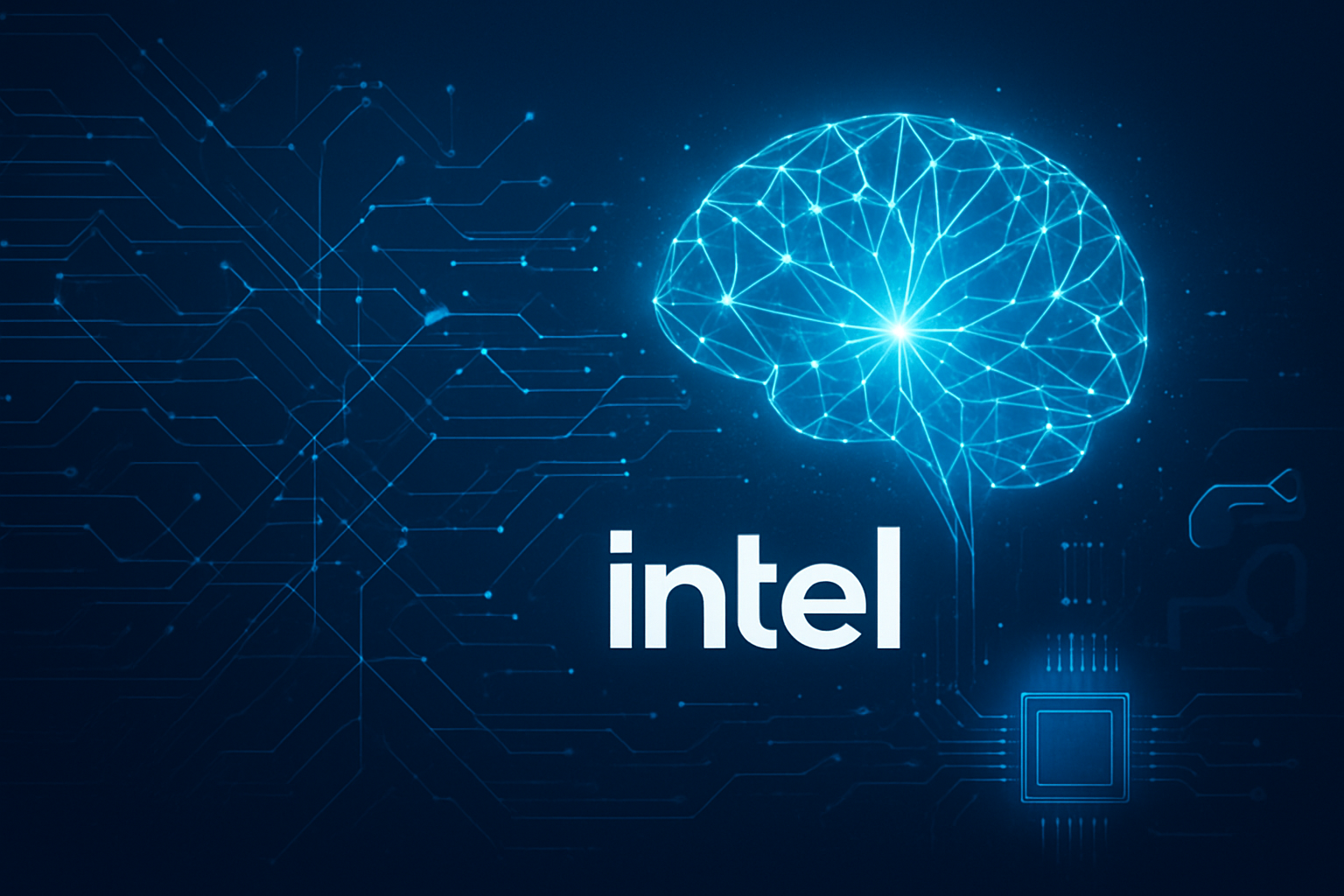
Initial reactions from the AI research community and industry experts are a mix of cautious optimism and skepticism. Many acknowledge the strategic importance of Intel's re-entry and the pragmatic approach to cost and power efficiency. However, skepticism persists regarding Intel's ability to execute and significantly challenge established leaders, given past struggles in the AI accelerator market and the perceived lag in its GPU roadmap compared to rivals.

    Reshaping the AI Landscape: Implications for Companies and Competitors

    The introduction of 'Crescent Island' is poised to create ripple effects across the AI industry, impacting tech giants, AI companies, and startups alike. "Token-as-a-service" providers, in particular, stand to benefit immensely from the chip's focus on "token economics" and cost efficiency, enabling them to offer more competitive pricing for AI model inference. AI startups and enterprises with budget constraints, needing to deploy memory-intensive LLMs without the prohibitive capital expenditure of HBM-based GPUs or liquid cooling, will find 'Crescent Island' a compelling and more accessible solution. Furthermore, its energy efficiency and suitability for air-cooled servers make it attractive for edge AI and distributed AI deployments, where energy consumption and cooling are critical factors.

    For tech giants like Microsoft (NASDAQ: MSFT), Google (NASDAQ: GOOGL), and AWS (NASDAQ: AMZN), 'Crescent Island' offers a crucial diversification of the AI chip supply chain. While Google has its custom TPUs and Microsoft heavily invests in custom silicon and partners with Nvidia, Intel's cost-effective inference chip could provide an attractive alternative for specific inference workloads within their cloud platforms. AWS, which already has a multi-year partnership with Intel for custom AI chips, could integrate 'Crescent Island' into its offerings, providing customers with more diverse and cost-optimized inference services. This increased competition could potentially reduce their reliance on a single vendor for all AI acceleration needs.

    Intel's re-entry with 'Crescent Island' signifies a renewed effort to regain AI credibility, strategically targeting the lucrative inference segment. By prioritizing cost-efficiency and a differentiated memory strategy, Intel aims to carve out a distinct advantage against Nvidia's HBM-centric training dominance and AMD's competing MI series. Nvidia, while maintaining its near-monopoly in AI training, faces a direct challenge in the high-growth inference segment. Interestingly, Nvidia's $5 billion investment in Intel, acquiring a 4% stake, suggests a complex relationship of both competition and collaboration. For AMD, 'Crescent Island' intensifies competition, particularly for customers seeking more cost-effective and energy-efficient inference solutions, pushing AMD to continue innovating in its performance-per-watt and pricing strategies. This development could lower the entry barrier for AI deployment, accelerate AI adoption across industries, and potentially drive down pricing for high-volume AI inference tasks, making AI inference more of a commodity service.

    Wider Significance and AI's Evolving Landscape

    'Crescent Island' fits squarely into the broader AI landscape's current trends, particularly the escalating demand for inference capabilities as AI models become ubiquitous. As the computational demands for running trained models increasingly outpace those for training, Intel's explicit focus on inference addresses a critical and growing need, especially for "token-as-a-service" providers and real-time AI applications. The chip's emphasis on cost-efficiency and accessibility, driven by its LPDDR5X memory choice, aligns with the industry's push to democratize AI, making advanced capabilities more attainable for a wider range of businesses and developers. Furthermore, Intel's commitment to an open and modular ecosystem, coupled with a unified software stack, supports the broader trend towards open standards and greater interoperability in AI systems, reducing vendor lock-in and fostering innovation.

    The wider impacts of 'Crescent Island' could include increased competition and innovation within the AI accelerator market, potentially leading to more favorable pricing and a diverse array of hardware options for customers. By offering a cost-effective solution for inference, it could significantly lower the barrier to entry for deploying large language models and "agentic AI" at scale, accelerating AI adoption across various industries. However, several challenges loom. Intel's GPU roadmap still lags behind the rapid advancements of rivals, and dislodging Nvidia from its dominant position will be formidable. The LPDDR5X memory, while cost-effective, is generally slower than HBM, which might limit its appeal for certain high-bandwidth-demanding inference workloads. Competing with Nvidia's deeply entrenched CUDA ecosystem also remains a significant hurdle.

    In terms of historical significance, while 'Crescent Island' may not represent a foundational architectural shift akin to the advent of GPUs for parallel processing (Nvidia CUDA) or the introduction of specialized AI accelerators like Google's TPUs, it marks a significant market and strategic breakthrough for Intel. It signals a determined effort to capture a crucial segment of the AI market (inference) by focusing on cost-efficiency, open standards, and a comprehensive software approach. Its impact lies in potentially increasing competition, fostering broader AI adoption through affordability, and diversifying the hardware options available for deploying next-generation AI models, especially those driving the explosion of LLMs.

    Future Developments and Expert Outlook

    In the near term (H2 2026 – 2027), the focus for 'Crescent Island' will be on customer sampling, gathering feedback, refining the product, and securing initial adoption. Intel will also be actively refining its open-source software stack to ensure seamless compatibility with the Xe3P architecture and ease of deployment across popular AI frameworks. Intel has committed to an annual release cadence for its AI data center GPUs, indicating a sustained, long-term strategy to keep pace with competitors. This commitment is crucial for establishing Intel as a consistent and reliable player in the AI hardware space. Long-term, 'Crescent Island' is a cornerstone of Intel's vision for a unified AI ecosystem, integrating its diverse hardware offerings with an open-source software stack to simplify developer experiences and optimize performance across its platforms.

    Potential applications for 'Crescent Island' are vast, extending across generative AI chatbots, video synthesis, and edge-based analytics. Its generous 160GB of LPDDR5X memory makes it particularly well-suited for handling the massive datasets and memory throughput required by large language models and multimodal workloads. Cloud providers and enterprise data centers will find its cost optimization, performance-per-watt efficiency, and air-cooled operation attractive for deploying LLMs without the higher costs associated with liquid-cooled systems or more expensive HBM. However, significant challenges remain, particularly in catching up to established leaders and overcoming perception hurdles, who are already looking to HBM4 for their next-generation processors. The perception of LPDDR5X as "slower memory" compared to HBM also needs to be overcome by demonstrating compelling real-world "performance per dollar."

    Experts predict intense competition and significant diversification in the AI chip market, which is projected to surpass $150 billion in 2025 and potentially reach $1.3 trillion by 2030. 'Crescent Island' is seen as Intel's "bold bet," focusing on open ecosystems, energy efficiency, and an inference-first performance strategy, playing to Intel's strengths in integration and cost-efficiency. This positions it as a "right-sized, right-priced" solution, particularly for "tokens-as-a-service" providers and enterprises. While challenging Nvidia's dominance, experts note that Intel's success hinges on its ability to deliver on promised power efficiency, secure early adopters, and overcome the maturity advantage of Nvidia's CUDA ecosystem. Its success or failure will be a "very important test of Intel's long-term relevance in AI hardware." Beyond competition, AI itself is expected to become the "backbone of innovation" within the semiconductor industry, optimizing chip design and manufacturing processes, and inspiring new architectural paradigms specifically for AI workloads.

    A New Chapter in the AI Chip Race

    Intel's 'Crescent Island' AI chip marks a pivotal moment in the escalating AI hardware race, signaling a determined and strategic re-entry into a market segment Intel can ill-afford to ignore. By focusing squarely on AI inference, prioritizing "performance per dollar" through its Xe3P architecture and 160GB LPDDR5X memory, and championing an open ecosystem, Intel is carving out a differentiated path. This approach aims to democratize access to powerful AI inference capabilities, offering a compelling alternative to HBM-laden, high-cost solutions from rivals like AMD and Nvidia. The chip's potential to lower the barrier to entry for LLM deployment and its suitability for cost-sensitive, air-cooled data centers could significantly accelerate AI adoption across various industries.

    The significance of 'Crescent Island' lies not just in its technical specifications, but in Intel's renewed commitment to an annual GPU release cadence and a unified software stack. This comprehensive strategy, backed by strategic partnerships (including Nvidia's investment), positions Intel to regain market relevance and intensify competition. While challenges remain, particularly in catching up to established leaders and overcoming perception hurdles, 'Crescent Island' represents a crucial test of Intel's ability to execute its vision. The coming weeks and months, leading up to customer sampling in late 2026 and the full market launch in 2027, will be critical. The industry will be closely watching for concrete performance benchmarks, market acceptance, and the continued evolution of Intel's AI ecosystem as it strives to redefine the economics of AI inference and reshape the competitive landscape.


    This content is intended for informational purposes only and represents analysis of current AI developments.

    TokenRing AI delivers enterprise-grade solutions for multi-agent AI workflow orchestration, AI-powered development tools, and seamless remote collaboration platforms.
    For more information, visit https://www.tokenring.ai/.

  • TSMC’s Q3 2025 Earnings Propel AI Revolution Amid Bullish Outlook

    TSMC’s Q3 2025 Earnings Propel AI Revolution Amid Bullish Outlook

    Taipei, Taiwan – October 14, 2025 – Taiwan Semiconductor Manufacturing Company (NYSE: TSM), the undisputed titan of the semiconductor foundry industry, is poised to announce a blockbuster third quarter for 2025. Widespread anticipation and a profoundly bullish outlook are sweeping through the tech world, driven by the insatiable global demand for artificial intelligence (AI) chips. Analysts are projecting record-breaking revenue and net profit figures, cementing TSMC's indispensable role as the "unseen architect" of the AI supercycle and signaling a robust health for the broader tech ecosystem.

    The immediate significance of TSMC's anticipated Q3 performance cannot be overstated. As the primary manufacturer of the most advanced processors for leading AI companies, TSMC's financial health serves as a critical barometer for the entire AI and high-performance computing (HPC) landscape. A strong report will not only validate the ongoing AI supercycle but also reinforce TSMC's market leadership and its pivotal role in enabling the next generation of technological innovation.

    Analyst Expectations Soar Amidst AI-Driven Demand and Strategic Pricing

    The financial community is buzzing with optimism for TSMC's Q3 2025 earnings, with specific forecasts painting a picture of exceptional growth. Analysts widely anticipated TSMC's Q3 2025 revenue to fall between $31.8 billion and $33 billion, representing an approximate 38% year-over-year increase at the midpoint. Preliminary sales data confirmed a strong performance, with Q3 revenue reaching NT$989.918 billion ($32.3 billion), exceeding most analyst expectations. This robust growth is largely attributed to the relentless demand for AI accelerators and high-end computing components.

    Net profit projections are equally impressive. A consensus among analysts, including an LSEG SmartEstimate compiled from 20 analysts, forecast a net profit of NT$415.4 billion ($13.55 billion) for the quarter. This would mark a staggering 28% increase from the previous year, setting a new record for the company's highest quarterly profit in its history and extending its streak to a seventh consecutive quarter of profit growth. Wall Street analysts generally expected earnings per share (EPS) of $2.63, reflecting a 35% year-over-year increase, with the Zacks Consensus Estimate adjusted upwards to $2.59 per share, indicating a 33.5% year-over-year growth.

    A key driver of this financial strength is TSMC's improving pricing power for its advanced nodes. Reports indicate that TSMC plans for a 5% to 10% price hike for advanced node processes in 2025. This increase is primarily a response to rising production costs, particularly at its new Arizona facility, where manufacturing expenses are estimated to be at least 30% higher than in Taiwan. However, tight production capacity for cutting-edge technologies also contributes to this upward price pressure. Major clients such as Apple (NASDAQ: AAPL), Advanced Micro Devices (NASDAQ: AMD), and Nvidia (NASDAQ: NVDA), who are heavily reliant on these advanced nodes, are expected to absorb these higher manufacturing costs, demonstrating TSMC's indispensable position. For instance, TSMC has set the price for its upcoming 2nm wafers at approximately $30,000 each, a 15-20% increase over the average $25,000-$27,000 price for its 3nm process.

    TSMC's technological leadership and dominance in advanced semiconductor manufacturing processes are crucial to its Q3 success. Its strong position in 3-nanometer (3nm) and 5-nanometer (5nm) manufacturing nodes is central to the revenue surge, with these advanced nodes collectively representing 74% of total wafer revenue in Q2 2025. Production ramp-up of 3nm chips, vital for AI and HPC devices, is progressing faster than anticipated, with 3nm lines operating at full capacity. The "insatiable demand" for AI chips, particularly from companies like Nvidia, Apple, AMD, and Broadcom (NASDAQ: AVGO), continues to be the foremost driver, fueling substantial investments in AI infrastructure and cloud computing.

    TSMC's Indispensable Role: Reshaping the AI and Tech Landscape

    TSMC's strong Q3 2025 performance and bullish outlook are poised to profoundly impact the artificial intelligence and broader tech industry, solidifying its role as the foundational enabler of the AI supercycle. The company's unique manufacturing capabilities mean that its success directly translates into opportunities and challenges across the industry.

    Major beneficiaries of TSMC's technological prowess include the leading players in AI and high-performance computing. Nvidia, for example, is heavily dependent on TSMC for its cutting-edge GPUs, such as the H100 and upcoming architectures like Blackwell and Rubin, with TSMC's advanced CoWoS (Chip-on-Wafer-on-Substrate) packaging technology being indispensable for integrating high-bandwidth memory. Apple relies on TSMC's 3nm process for its M4 and M5 chips, powering on-device AI capabilities. Advanced Micro Devices (NASDAQ: AMD) utilizes TSMC's advanced packaging and leading-edge nodes for its next-generation data center GPUs and EPYC CPUs, positioning itself as a strong contender in the HPC market. Hyperscalers like Alphabet (NASDAQ: GOOGL), Amazon (NASDAQ: AMZN), Meta Platforms (NASDAQ: META), and Microsoft (NASDAQ: MSFT) are increasingly designing their own custom AI silicon (ASICs) and are significant customers for TSMC's advanced nodes, including the upcoming 2nm process.

    The competitive implications for major AI labs and tech companies are significant. TSMC's indispensable position centralizes the AI hardware ecosystem around a select few dominant players who can secure access to its advanced manufacturing capabilities. This creates substantial barriers to entry for newer firms or those without significant capital or strategic partnerships. While Intel (NASDAQ: INTC) is working to establish its own competitive foundry business, TSMC's advanced-node manufacturing capabilities are widely recognized as superior, creating a significant gap. The continuous push for more powerful and energy-efficient AI chips directly disrupts existing products and services that rely on older, less efficient hardware. Companies unable to upgrade their AI infrastructure or adapt to the rapid advancements risk falling behind in performance, cost-efficiency, and capabilities.

    In terms of market positioning, TSMC maintains its undisputed position as the world's leading pure-play semiconductor foundry, holding over 70.2% of the global pure-play foundry market and an even higher share in advanced AI chip production. Its technological prowess, mastering cutting-edge process nodes (3nm, 2nm, A16, A14 for 2028) and innovative packaging solutions (CoWoS, SoIC), provides an unparalleled strategic advantage. The 2nm (N2) process, featuring Gate-All-Around (GAA) nanosheet transistors, is on track for mass production in the second half of 2025, with demand already exceeding initial capacity. Furthermore, TSMC is pursuing a "System Fab" strategy, offering a comprehensive suite of interconnected technologies, including advanced 3D chip stacking and packaging (TSMC 3DFabric®) to enable greater performance and power efficiency for its customers.

    Wider Significance: AI Supercycle Validation and Geopolitical Crossroads

    TSMC's exceptional Q3 2025 performance is more than just a corporate success story; it is a profound validation of the ongoing AI supercycle and a testament to the transformative power of advanced semiconductor technology. The company's financial health is a direct reflection of the global AI chip market's explosive growth, projected to increase from an estimated $123.16 billion in 2024 to $311.58 billion by 2029, with AI chips contributing over $150 billion to total semiconductor sales in 2025 alone.

    This success highlights several key trends in the broader AI landscape. Hardware has re-emerged as a strategic differentiator, with custom AI chips (NPUs, TPUs, specialized AI accelerators) becoming ubiquitous. TSMC's dominance in advanced nodes and packaging is crucial for the parallel processing, high data transfer speeds, and energy efficiency required by modern AI accelerators and large language models. There's also a significant shift towards edge AI and energy efficiency, as AI deployments scale and demand low-power, high-efficiency chips for applications from autonomous vehicles to smart cameras.

    The broader impacts are substantial. TSMC's growth acts as a powerful economic catalyst, driving innovation and investment across the entire tech ecosystem. Its capabilities accelerate the iteration of chip technology, compelling companies to continuously upgrade their AI infrastructure. This profoundly reshapes the competitive landscape for AI companies, creating clear beneficiaries among major tech giants that rely on TSMC for their most critical AI and high-performance chips.

    However, TSMC's centrality to the AI landscape also highlights significant vulnerabilities and concerns. The "extreme supply chain concentration" in Taiwan, where over 90% of the world's most advanced chips are manufactured by TSMC and Samsung (KRX: 005930), creates a critical single point of failure. Escalating geopolitical tensions in the Taiwan Strait pose a severe risk, with potential military conflict or economic blockade capable of crippling global AI infrastructure. TSMC is actively trying to mitigate this by diversifying its manufacturing footprint with significant investments in the U.S. (Arizona), Japan, and Germany. The U.S. CHIPS Act is also a strategic initiative to secure domestic semiconductor production and reduce reliance on foreign manufacturing. Beyond Taiwan, the broader AI chip supply chain relies on a concentrated "triumvirate" of Nvidia (chip designs), ASML (AMS: ASML) (precision lithography equipment), and TSMC (manufacturing), creating further single points of failure.

    Comparing this to previous AI milestones, the current growth phase, heavily reliant on TSMC's manufacturing prowess, represents a unique inflection point. Unlike previous eras where hardware was more of a commodity, the current environment positions advanced hardware as a "strategic differentiator." This "sea change" in generative AI is being compared to fundamental technology shifts like the internet, mobile, and cloud computing, indicating a foundational transformation across industries.

    Future Horizons: Unveiling Next-Generation AI and Global Expansion

    Looking ahead, TSMC's future developments are characterized by an aggressive technology roadmap, continued advancements in manufacturing and packaging, and strategic global diversification, all geared towards sustaining its leadership in the AI era.

    In the near term, TSMC's 3nm (N3 family) process, already in volume production, will remain a workhorse for current high-performance AI chips. However, the true game-changer will be the mass production of the 2nm (N2) process node, ramping up in late 2025. Major clients like Apple, Advanced Micro Devices (NASDAQ: AMD), Intel (NASDAQ: INTC), Nvidia (NASDAQ: NVDA), Qualcomm (NASDAQ: QCOM), and MediaTek are expected to utilize this node, which promises a 25-30% reduction in power consumption or a 10-15% increase in performance compared to 3nm chips. TSMC projects initial 2nm capacity to reach over 100,000 wafers per month in 2026. Beyond 2nm, the A16 (1.6nm-class) technology is slated for production readiness in late 2026, followed by A14 (1.4nm-class) for mass production in the second half of 2028, further pushing the boundaries of chip density and efficiency.

    Advanced packaging technologies are equally critical. TSMC is aggressively expanding its CoWoS (Chip-on-Wafer-on-Substrate) advanced packaging capacity, aiming to quadruple its output by the end of 2025 and further increase it to 130,000 wafers per month by 2026 to meet surging AI demand. Innovations like CoWoS-L (expected 2027) and SoIC (System-on-Integrated-Chips) will enable even denser chip stacking and integration, crucial for the complex architectures of future AI accelerators.

    The ongoing advancements in AI chips are enabling a vast array of new and enhanced applications. Beyond data centers and cloud computing, there is a significant shift towards deploying AI at the edge, including autonomous vehicles, industrial robotics, smart cameras, mobile devices, and various IoT devices, demanding low-power, high-efficiency chips like Neural Processing Units (NPUs). AI-enabled PCs are expected to constitute 43% of all shipments by the end of 2025. In healthcare, AI chips are crucial for medical imaging systems with superhuman accuracy and powering advanced computations in scientific research and drug discovery.

    Despite the rapid progress, several significant challenges need to be overcome. Manufacturing complexity and cost remain immense, with a new fabrication plant costing $15B-$20B. Design and packaging hurdles, such as optimizing performance while reducing immense power consumption and managing heat dissipation, are critical. Supply chain and geopolitical risks, particularly the concentration of advanced manufacturing in Taiwan, continue to be a major concern, driving TSMC's strategic global expansion into the U.S. (Arizona), Japan, and Germany. The immense energy consumption of AI infrastructure also raises significant environmental concerns, making energy efficiency a crucial area for innovation.

    Industry experts are highly optimistic, predicting TSMC will remain the "indispensable architect of the AI supercycle," with its market dominance and growth trajectory defining the future of AI hardware. The global AI chip market is projected to skyrocket to an astonishing $311.58 billion by 2029, or around $295.56 billion by 2030, with a Compound Annual Growth Rate (CAGR) of 33.2% from 2025 to 2030. The intertwining of AI and semiconductors is projected to contribute more than $15 trillion to the global economy by 2030.

    A New Era: TSMC's Enduring Legacy and the Road Ahead

    TSMC's anticipated Q3 2025 earnings mark a pivotal moment, not just for the company, but for the entire technological landscape. The key takeaway is clear: TSMC's unparalleled leadership in advanced semiconductor manufacturing is the bedrock upon which the current AI revolution is being built. The strong revenue growth, robust net profit projections, and improving pricing power are all direct consequences of the "insatiable demand" for AI chips and the company's continuous innovation in process technology and advanced packaging.

    This development holds immense significance in AI history, solidifying TSMC's role as the "unseen architect" that enables breakthroughs across every facet of artificial intelligence. Its pure-play foundry model has fostered an ecosystem where innovation in chip design can flourish, driving the rapid advancements seen in AI models today. The long-term impact on the tech industry is profound, centralizing the AI hardware ecosystem around TSMC's capabilities, accelerating hardware obsolescence, and dictating the pace of technological progress. However, it also highlights the critical vulnerabilities associated with supply chain concentration, especially amidst escalating geopolitical tensions.

    In the coming weeks and months, all eyes will be on TSMC's official Q3 2025 earnings report and the subsequent earnings call on October 16, 2025. Investors will be keenly watching for any upward revisions to full-year 2025 revenue forecasts and crucial fourth-quarter guidance. Geopolitical developments, particularly concerning US tariffs and trade relations, remain a critical watch point, as proposed tariffs or calls for localized production could significantly impact TSMC's operational landscape. Furthermore, observers will closely monitor the progress and ramp-up of TSMC's global manufacturing facilities in Arizona, Japan, and Germany, assessing their impact on supply chain resilience and profitability. Updates on the development and production scale of the 2nm process and advancements in critical packaging technologies like CoWoS and SoIC will also be key indicators of TSMC's continued technological leadership and the trajectory of the AI supercycle.


    This content is intended for informational purposes only and represents analysis of current AI developments.

    TokenRing AI delivers enterprise-grade solutions for multi-agent AI workflow orchestration, AI-powered development tools, and seamless remote collaboration platforms.
    For more information, visit https://www.tokenring.ai/.