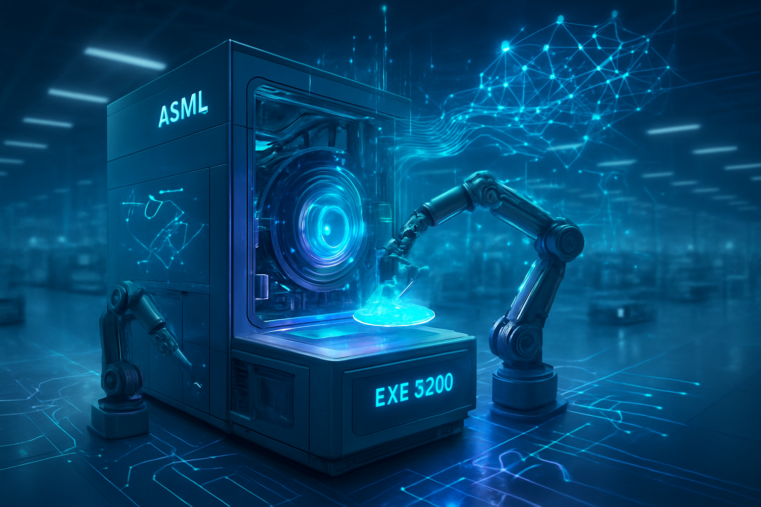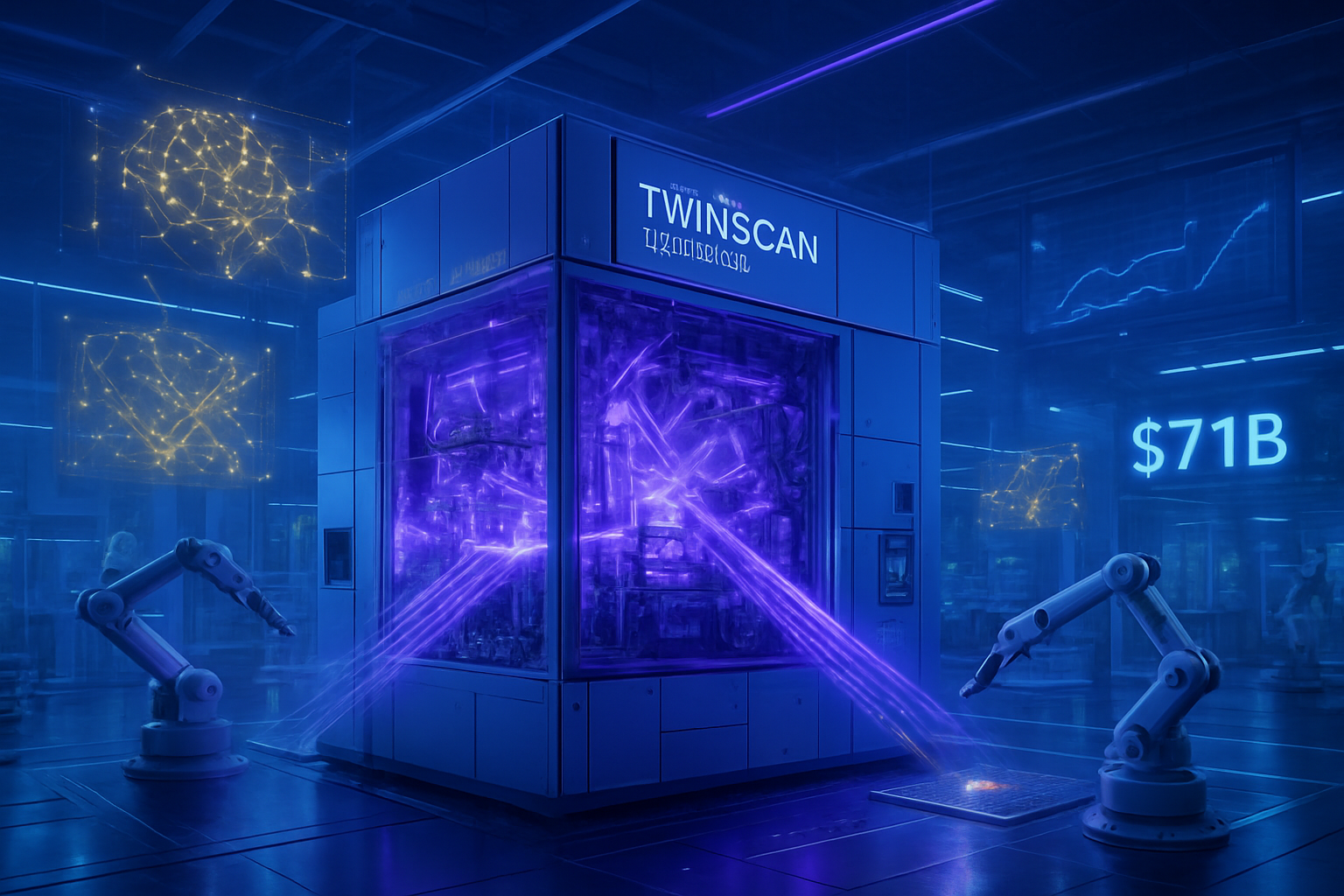
In a definitive signal of the semiconductor industry’s direction, ASML (NASDAQ: ASML) has solidified its 2030 revenue target at a staggering $71 billion (€60 billion), underpinned by the aggressive rollout of its High-NA (Numerical Aperture) EUV lithography systems. This announcement comes as the Dutch technology giant marks a historic milestone: the successful delivery and installation of the first commercial-grade TWINSCAN EXE:5200B systems to industry leaders Intel (NASDAQ: INTC) and SK Hynix (KRX: 000660). As of January 30, 2026, ASML stands at the center of the global AI arms race, with its order backlog swelling to record levels as chipmakers scramble for the tools necessary to manufacture the next generation of AI accelerators and high-bandwidth memory.
The transition to High-NA EUV represents more than just an incremental upgrade; it is a fundamental shift in how the world’s most advanced silicon is produced. Driven by an insatiable demand for AI-capable hardware, ASML’s roadmap now bridges the gap between today’s 3-nanometer processes and the upcoming "Angstrom era." With its recent quarterly bookings nearly doubling analyst expectations, ASML has transformed from a equipment supplier into the ultimate gatekeeper of the AI economy, ensuring that the hardware requirements of generative AI models can be met through unprecedented transistor density and energy efficiency.
The Technical Leap: Decoding the EXE:5200B
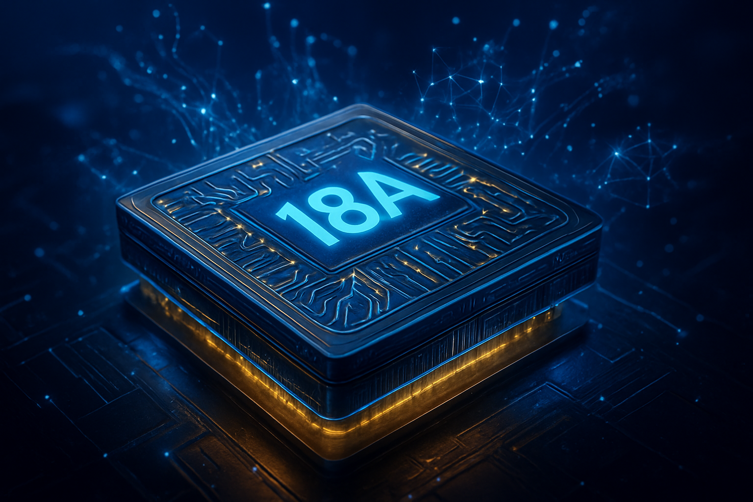
The core of ASML’s growth strategy lies in the TWINSCAN EXE:5200B, the company’s first "production-worthy" High-NA system. Unlike the previous standard EUV (Low-NA) machines that utilized a 0.33 numerical aperture, the EXE:5200B jumps to 0.55 NA. This technical shift allows for a resolution of just 8nm, a significant improvement over the 13nm limit of previous systems. This leap enables a 2.9x increase in transistor density, allowing engineers to pack nearly three times as many components into the same silicon footprint. For the AI research community, this means the potential for dramatically more powerful NPUs (Neural Processing Units) and GPUs that can handle trillions of parameters with lower power consumption.
The most critical advantage of the EXE:5200B is its ability to perform "single-exposure" lithography for features that previously required complex multi-patterning techniques. Multi-patterning—essentially passing a wafer through a machine multiple times to etch a single layer—is notorious for increasing defects and manufacturing cycle times. By achieving these fine details in a single pass, High-NA EUV significantly reduces the complexity of 2nm and 1.4nm (Intel 14A) process nodes. Initial feedback from engineers at Intel's Oregon facility suggests that the 0.7nm overlay accuracy of the 5200B is providing the precision necessary to align the dozens of layers required for modern 3D transistor architectures, such as Gate-All-Around (GAA) FETs.
Reshaping the Competitive Landscape
The early delivery of these systems has already begun to shift the strategic balance among the world's leading chipmakers. Intel (NASDAQ: INTC) has moved aggressively to reclaim its "process leadership" crown, being the first to complete acceptance testing of the EXE:5200B in late 2025. By integrating High-NA early, Intel aims to bypass the mid-generation struggles of its competitors, targeting risk production of its 14A node by 2027. This move is seen as a high-stakes bet to draw major AI clients away from TSMC (NYSE: TSM), which has taken a more cautious, "fast-follower" approach to High-NA adoption due to the machine's estimated $380 million price tag.
In the memory sector, the arrival of the EXE:5200B at SK Hynix (KRX: 000660) and Samsung Electronics (KRX: 005930) marks a pivotal moment for AI infrastructure. For the first time in ASML’s history, memory chip orders have surpassed logic orders, accounting for 56% of the company's recent bookings. This is directly attributable to the High-Bandwidth Memory (HBM) required by Nvidia (NASDAQ: NVDA) and other AI accelerator designers. HBM4 and HBM5 require the ultra-fine resolution of High-NA to manage the vertical stacking of memory layers and the high-speed interconnects that prevent data bottlenecks in large language model (LLM) training.
The Broader Significance: Moore’s Law in the AI Age
The $71 billion revenue target is a testament to the fact that "lithography intensity" is increasing. As chips become more complex, they require more EUV exposures per wafer. This trend effectively extends the life of Moore's Law, which many critics had pronounced dead a decade ago. By providing a path to the 1.4nm and 1nm nodes, ASML is ensuring that the hardware side of the AI revolution does not hit a scaling wall. The ability to print features at the angstrom level is the only way to keep up with the computational demands of future "Agentic AI" systems that will require real-time processing at the edge.
However, ASML’s dominance also highlights a growing concern regarding industry concentration. With a record backlog of €38.8 billion ($46.3 billion), the entire global tech sector is now dependent on a single company’s ability to manufacture and ship these massive, school-bus-sized machines. Any supply chain disruption or geopolitical tension—particularly concerning export controls to China—could have immediate, cascading effects on the availability of AI compute. The sheer cost and complexity of High-NA EUV are creating a "Rich-Club" of chipmakers, potentially pricing out smaller players and consolidating the power of the "Big Three" (Intel, TSMC, and Samsung).
The Road to 2030 and Beyond
Looking ahead, ASML is already laying the groundwork for life after High-NA. While the EXE:5200B is expected to be the workhorse of the late 2020s, the company has begun exploring "Hyper-NA" lithography, which would push numerical apertures beyond 0.75. Near-term, the focus remains on ramping up the production of the 5200B to meet the massive orders scheduled for 2026 and 2027. Experts predict that as the software side of AI matures, the demand for specialized, custom silicon (ASICs) will explode, further driving the need for the flexible, high-precision manufacturing that High-NA provides.
The challenges remain formidable. Each High-NA machine requires 250 crates and multiple cargo planes to transport, and the energy consumption of these tools is significant. ASML and its partners are under pressure to improve the sustainability of the lithography process, even as they push the limits of physics. As we move toward 2030, the integration of AI-driven "computational lithography"—where AI models predict and correct for optical distortions in real-time—will likely become as important as the physical lenses themselves.
A New Chapter in Silicon History
ASML’s journey toward its $71 billion goal is more than a financial success story; it is the heartbeat of modern technological progress. By successfully delivering the EXE:5200B to Intel and SK Hynix, ASML has proven that it can translate theoretical physics into a reliable industrial process. The massive backlog and the shift toward memory-heavy orders confirm that the AI boom is not a fleeting trend, but a structural shift in the global economy that requires a fundamental reimagining of semiconductor manufacturing.
In the coming weeks and months, the industry will be watching the yields of the first High-NA-produced wafers. If Intel and SK Hynix can demonstrate a significant performance-per-watt advantage over standard EUV, the pressure on TSMC and other foundry players to accelerate their High-NA adoption will become unbearable. For now, ASML remains the indispensable architect of the digital future, holding the keys to the most advanced tools ever created by humanity.
This content is intended for informational purposes only and represents analysis of current AI developments.
TokenRing AI delivers enterprise-grade solutions for multi-agent AI workflow orchestration, AI-powered development tools, and seamless remote collaboration platforms.
For more information, visit https://www.tokenring.ai/.