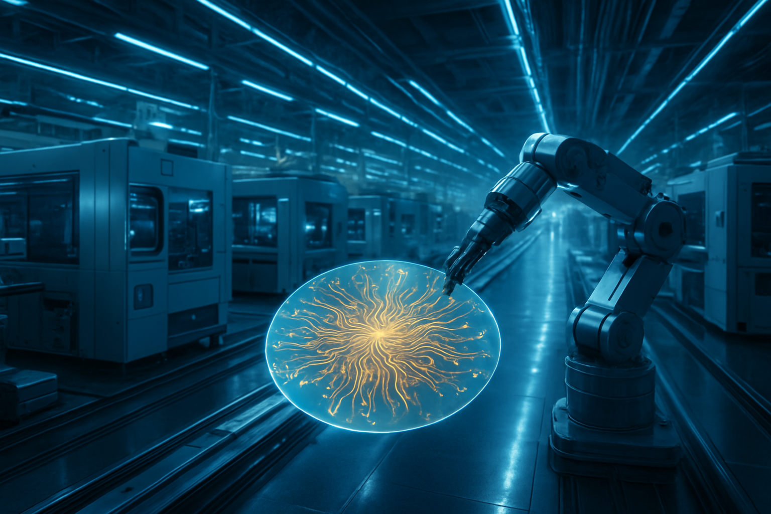
As the artificial intelligence revolution accelerates into 2026, the semiconductor industry is undergoing its most significant material shift in decades. The traditional organic materials that have anchored chip packaging for nearly thirty years—plastic resins and laminate-based substrates—have finally hit a physical limit, often referred to by engineers as the "warpage wall." In response, industry leaders Intel (NASDAQ:INTC) and Samsung (KRX:005930) have accelerated their transition to glass-core substrates, launching high-volume manufacturing lines that promise to reshape the physical architecture of AI data centers.
This transition is not merely a material upgrade; it is a fundamental architectural pivot required to build the massive "super-packages" that power next-generation AI workloads. By early 2026, these glass-based substrates have moved from experimental research to the backbone of frontier hardware. Intel has officially debuted its first commercial glass-core processors, while Samsung has synchronized its display and electronics divisions to create a vertically integrated supply chain. The implications are profound: glass allows for larger, more stable, and more efficient chips that can handle the staggering power and bandwidth demands of the world's most advanced large language models.
Engineering the "Warpage Wall": The Technical Leap to Glass
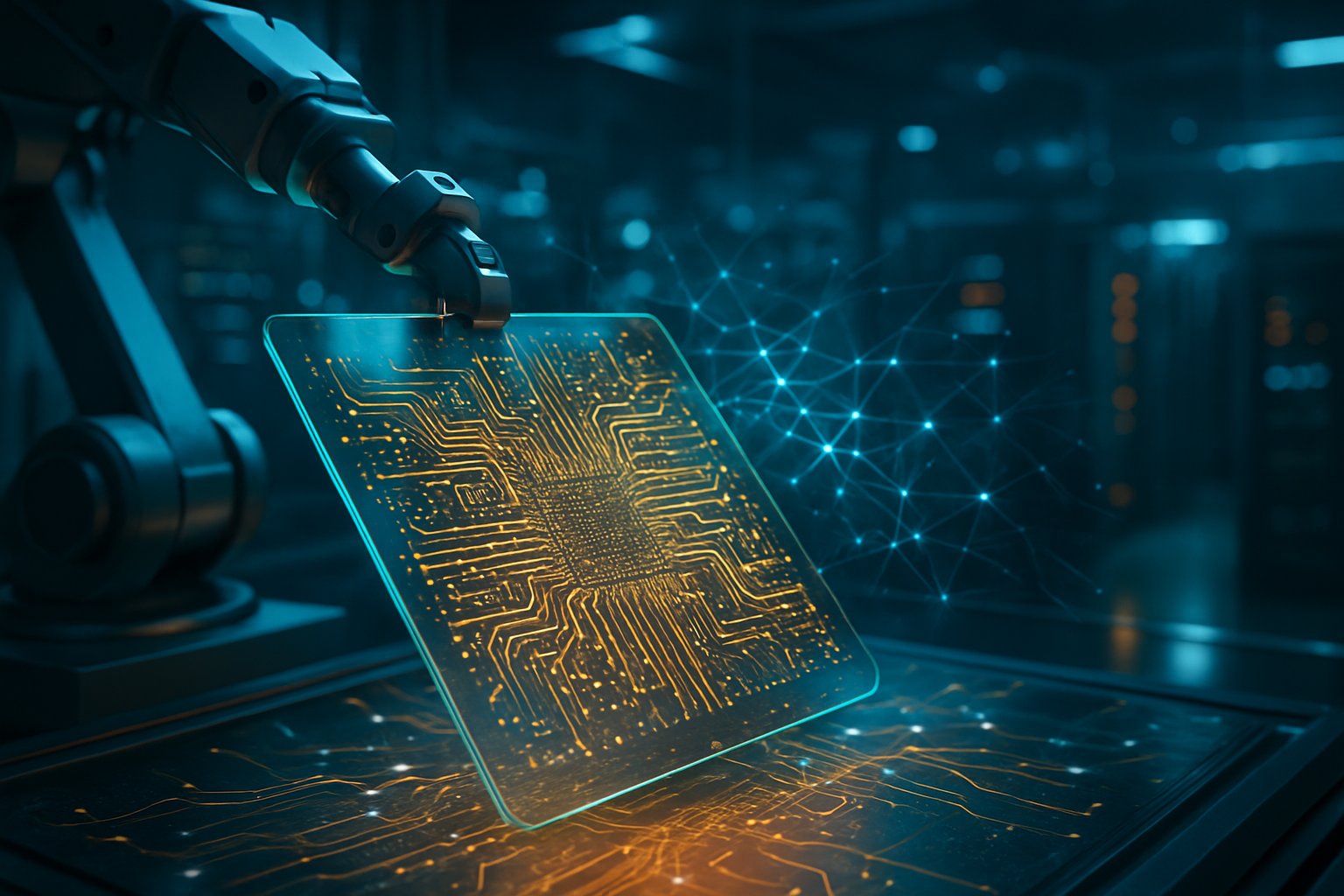
For decades, the industry relied on Ajinomoto Build-up Film (ABF) and organic substrates, but as AI chips grow to "reticle-busting" sizes, these materials tend to flex and bend—a phenomenon known as "potato-chipping." As of January 2026, the technical specifications of glass substrates have rendered organic materials obsolete for high-end AI accelerators. Glass provides a superior flatness with warpage levels measured at less than 20μm across a 100mm area, compared to the >50μm deviation typical of organic cores. This precision is critical for the ultra-fine lithography required to stitch together dozens of chiplets on a single module.
Furthermore, glass boasts a Coefficient of Thermal Expansion (CTE) that nearly matches silicon (3–5 ppm/°C). This alignment is vital for reliability; as chips heat and cool, organic substrates expand at a different rate than the silicon chips they carry, causing mechanical stress that can crack microscopic solder bumps. Glass eliminates this risk, enabling the creation of "super-packages" exceeding 100mm x 100mm. These massive modules integrate logic, networking, and HBM4 (High Bandwidth Memory) into a unified system. The introduction of Through-Glass Vias (TGVs) has also increased interconnect density by 10x, while the dielectric properties of glass have reduced power loss by up to 50%, allowing data to move faster and with less waste.
The Battle for Packaging Supremacy: Intel vs. Samsung vs. TSMC
The shift to glass has ignited a high-stakes competitive race between the world’s leading foundries. Intel (NASDAQ:INTC) has claimed the first-mover advantage, utilizing its advanced facility in Chandler, Arizona, to launch the Xeon 6+ "Clearwater Forest" processor. This marks the first time a mass-produced CPU has utilized a glass core. By pivoting early, Intel is positioning its "Foundry-first" model as a superior alternative for companies like NVIDIA (NASDAQ:NVDA) and Apple (NASDAQ:AAPL), who are currently facing supply constraints at other foundries. Intel’s strategy is to use glass as a differentiator to lure high-value customers who need the stability of glass for their 2027 and 2028 roadmaps.
Meanwhile, Samsung (KRX:005930) has leveraged its internal "Triple Alliance"—the combined expertise of Samsung Electro-Mechanics, Samsung Electronics, and Samsung Display. By repurposing high-precision glass-handling technology from its Gen-8.6 OLED production lines, Samsung has fast-tracked its pilot lines in Sejong, South Korea. Samsung is targeting full mass production by the second half of 2026, with a specific focus on AI ASICs (Application-Specific Integrated Circuits). In contrast, TSMC (NYSE:TSM) has maintained a more cautious approach, continuing to expand its organic CoWoS (Chip-on-Wafer-on-Substrate) capacity while developing its own Glass-based Fan-Out Panel-Level Packaging (FOPLP). While TSMC remains the ecosystem leader, the aggressive moves by Intel and Samsung represent the first serious threat to its packaging dominance in years.
Reshaping the Global AI Landscape and Supply Chain
The broader significance of the glass transition lies in its ability to unlock the "super-package" era. These are not just chips; they are entire systems-in-package (SiP) that would be physically impossible to manufacture on plastic. This development allows AI companies to pack more compute power into a single server rack, effectively extending the lifespan of current data center cooling and power infrastructures. However, this transition has not been without growing pains. Early 2026 has seen a "Glass Cloth Crisis," where a shortage of high-grade "T-glass" cloth from specialized suppliers like Nitto Boseki has led to a bidding war between tech giants, momentarily threatening the supply of even traditional high-end substrates.
This shift also carries geopolitical weight. The establishment of glass substrate facilities in the United States, such as the Absolics plant in Georgia (a subsidiary of SK Group), represents a significant step in "re-shoring" advanced packaging. For the first time in decades, a critical part of the semiconductor value chain is moving closer to the AI designers in Silicon Valley and Seattle. This reduces the strategic dependency on Taiwanese packaging facilities and provides a more resilient supply chain for the US-led AI sector, though experts warn that initial yields for glass remain lower (75–85%) than the mature organic processes (95%+).
The Road Ahead: Silicon Photonics and Integrated Optics
Looking toward 2027 and beyond, the adoption of glass substrates paves the way for the next great leap: integrated silicon photonics. Because glass is inherently transparent, it can serve as a medium for optical interconnects, allowing chips to communicate via light rather than copper wiring. This would virtually eliminate the heat generated by electrical resistance and reduce latency to near-zero. Research is already underway at Intel and Samsung to integrate laser-based communication directly into the glass core, a development that could revolutionize how large-scale AI clusters operate.
However, challenges remain. The industry must still standardize glass panel sizes—transitioning from the current 300mm format to larger 515mm x 510mm panels—to achieve better economies of scale. Additionally, the handling of glass requires a complete overhaul of factory automation, as glass is more brittle and prone to shattering during the manufacturing process than organic laminates. As these technical hurdles are cleared, analysts predict that glass substrates will capture nearly 30% of the advanced packaging market by the end of the decade.
Summary: A New Foundation for Artificial Intelligence
The transition to glass substrates marks the end of the organic era and the beginning of a new chapter in semiconductor history. By providing a platform that matches the thermal and physical properties of silicon, glass enables the massive, high-performance "super-packages" that the AI industry desperately requires to continue its current trajectory of growth. Intel (NASDAQ:INTC) and Samsung (KRX:005930) have emerged as the early leaders in this transition, each betting that their glass-core technology will define the next five years of compute.
As we move through 2026, the key metrics to watch will be the stabilization of manufacturing yields and the expansion of the glass supply chain. While the "Glass Cloth Crisis" serves as a reminder of the fragility of high-tech manufacturing, the momentum behind glass is undeniable. For the AI industry, glass is not just a material choice; it is the essential foundation upon which the next generation of digital intelligence will be built.
This content is intended for informational purposes only and represents analysis of current AI developments.
TokenRing AI delivers enterprise-grade solutions for multi-agent AI workflow orchestration, AI-powered development tools, and seamless remote collaboration platforms.
For more information, visit https://www.tokenring.ai/.