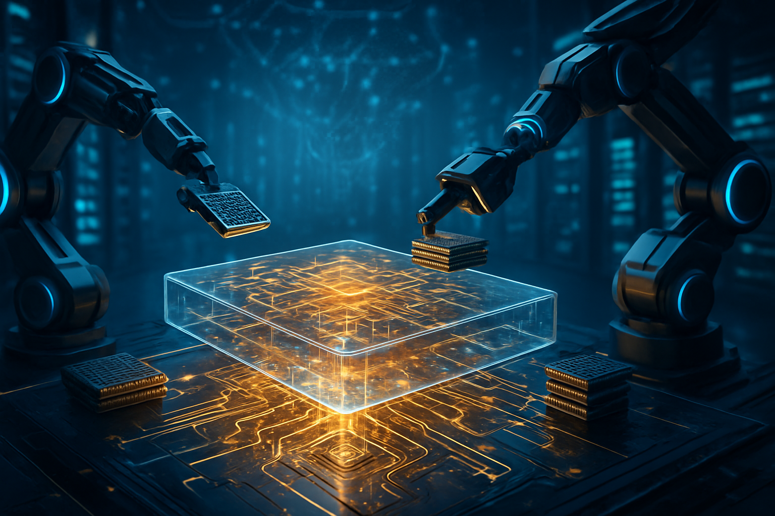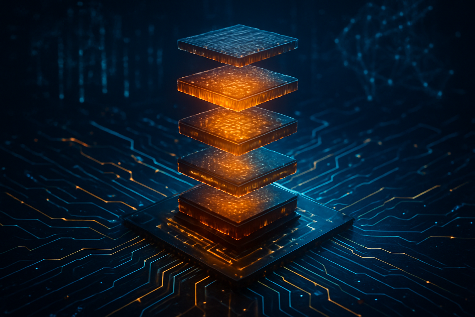
As of January 2026, the semiconductor industry has reached a definitive turning point, moving away from the monolithic processor designs that defined the last fifty years. The emergence of a robust "Chiplet Ecosystem," powered by the now-mature Universal Chiplet Interconnect Express (UCIe) 2.0 standard, has transformed chip design into a "Silicon Lego" architecture. This shift allows tech giants to assemble massive AI processors by "snapping together" specialized dies—memory, compute, and I/O—manufactured at different foundries, effectively shattering the constraints of single-wafer manufacturing.
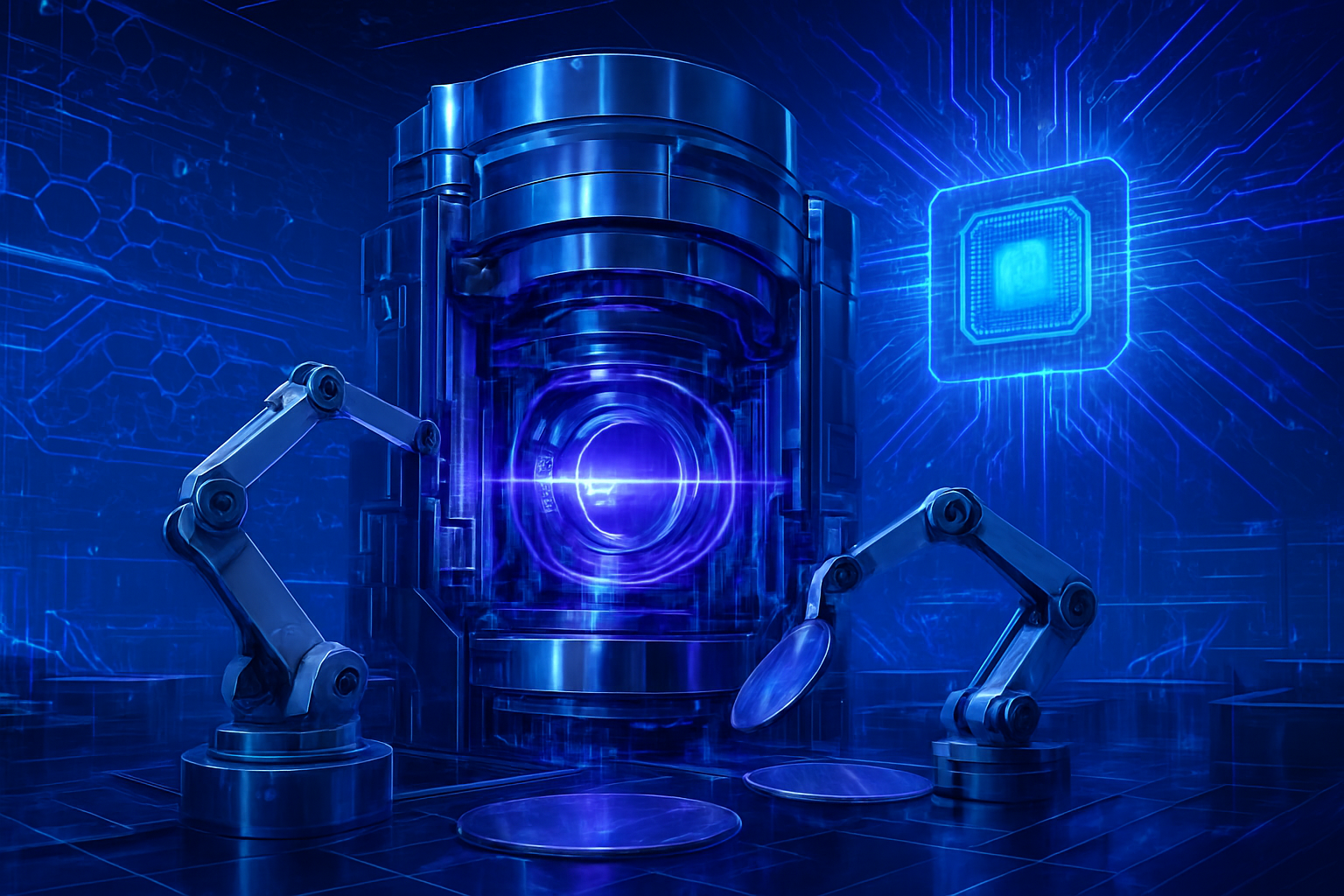
This transition is not merely an incremental upgrade; it represents the birth of 3D-native packaging. By 2026, the industry’s elite designers are no longer placing chiplets side-by-side on a flat substrate. Instead, they are stacking them vertically with atomic-level precision. This architectural leap is the primary driver behind the latest generation of AI superchips, which are currently enabling the training of trillion-parameter models with a fraction of the power required just two years ago.
The Technical Backbone: UCIe 2.0 and the 3D-Native Era
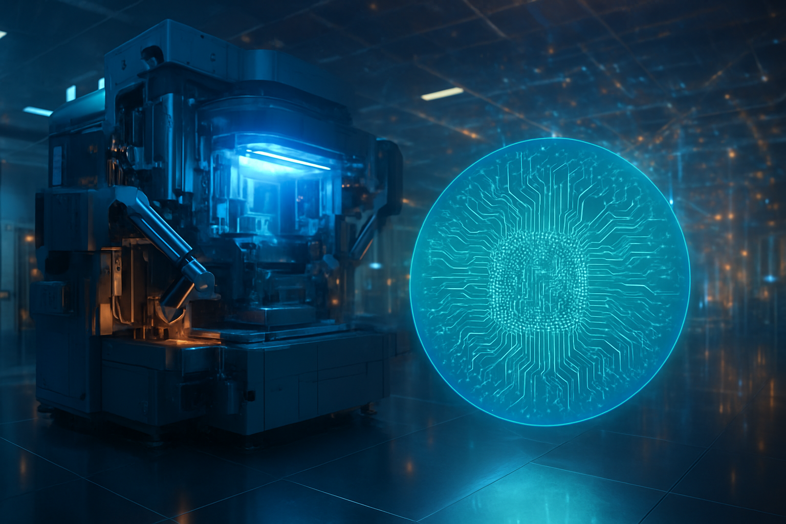
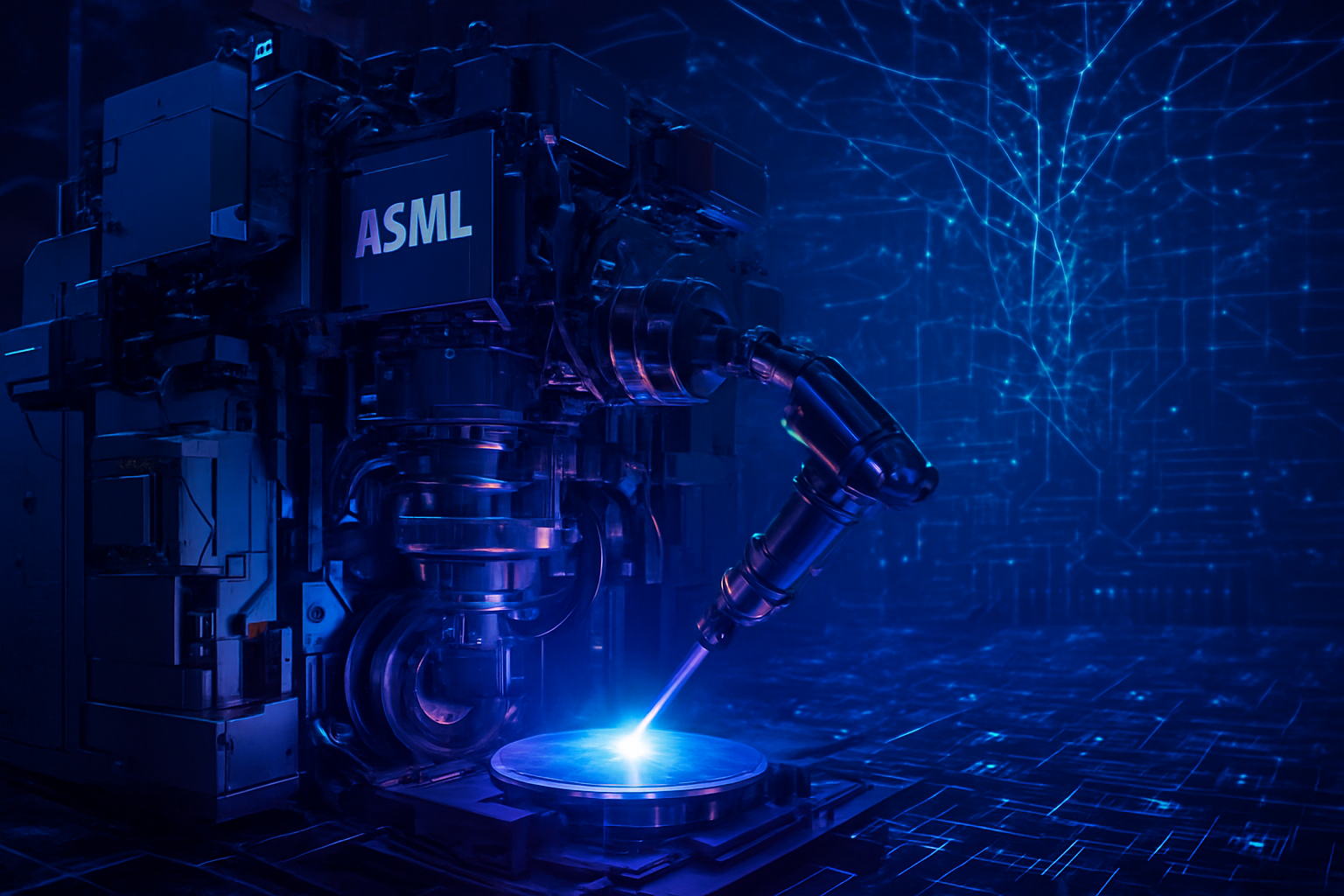
The technical heart of this revolution is the UCIe 2.0 specification, which has moved from its 2024 debut into full-scale industrial implementation this year. Unlike its predecessors, which focused on 2D and 2.5D layouts, UCIe 2.0 was the first standard built specifically for 3D-native stacking. The most critical breakthrough is the UCIe DFx Architecture (UDA), a vendor-agnostic management fabric. For the first time, a compute die from Intel (NASDAQ: INTC) can seamlessly "talk" to an I/O die from Taiwan Semiconductor Manufacturing Company (NYSE: TSM) for real-time testing and telemetry. This interoperability has solved the "known good die" (KGD) problem that previously haunted multi-vendor chiplet designs.
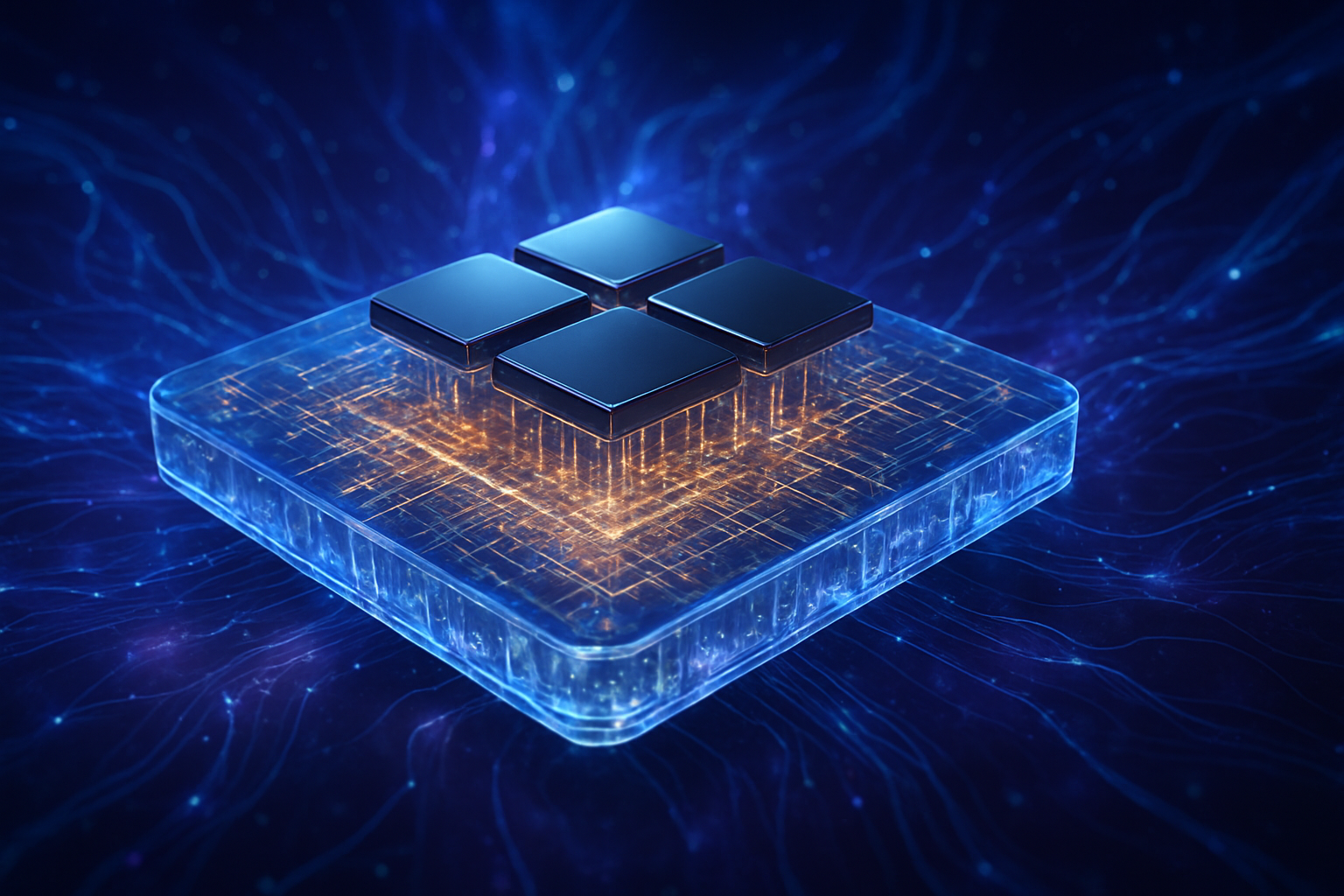
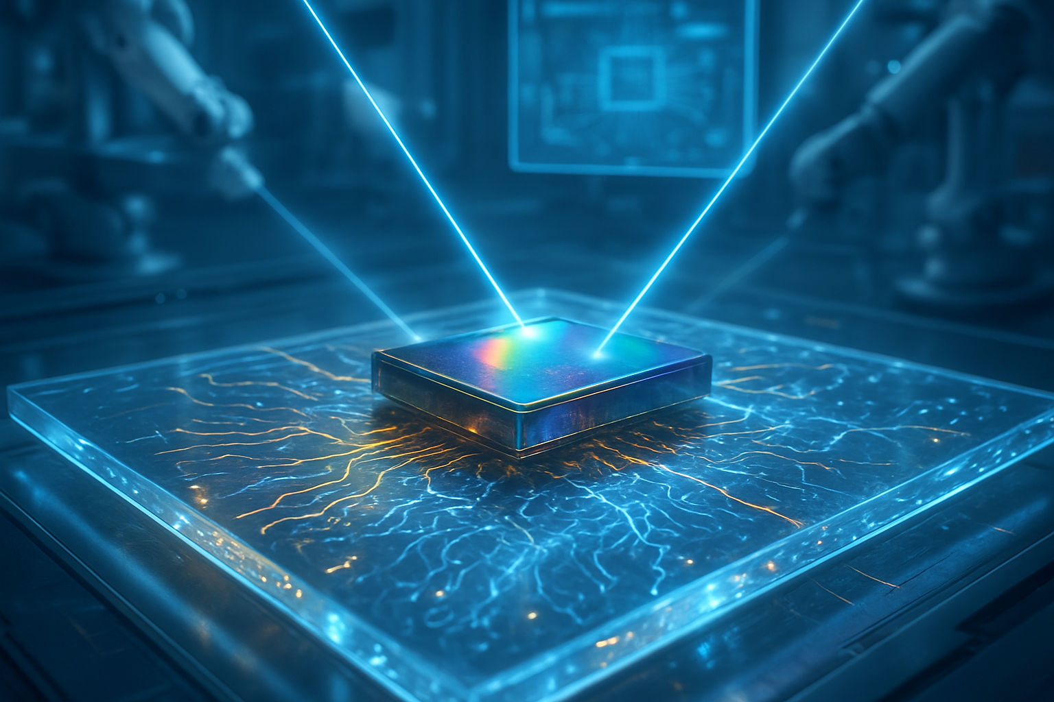
Furthermore, the shift to 3D-native design has moved interconnects from the edges of the chiplet to the entire surface area. Utilizing hybrid bonding—a process that replaces traditional solder bumps with direct copper-to-copper connections—engineers are now achieving bond pitches as small as 6 micrometers. This provides a 15-fold increase in interconnect density compared to the 2D "shoreline" approach. With bandwidth densities reaching up to 4 TB/s per square millimeter, the latency between stacked dies is now negligible, effectively making a stack of four chiplets behave like a single, massive piece of silicon.
Initial reactions from the AI research community have been overwhelming. Dr. Elena Vos, Chief Architect at an AI hardware consortium, noted that "the ability to mix-and-match a 2nm logic die with specialized 5nm analog I/O and HBM4 memory stacks using UCIe 2.0 has essentially decoupled architectural innovation from process node limitations. We are no longer waiting for a single foundry to perfect a whole node; we are building our own nodes in the package."
Strategic Reshuffling: Winners in the Chiplet Marketplace
This "Silicon Lego" approach has fundamentally altered the competitive landscape for tech giants and startups alike. NVIDIA (NASDAQ: NVDA) has leveraged this ecosystem to launch its Rubin R100 platform, which utilizes 3D-native stacking to achieve a 4x performance-per-watt gain over the previous Blackwell generation. By using UCIe 2.0, NVIDIA can integrate proprietary AI accelerators with third-party connectivity dies, allowing them to iterate on compute logic faster than ever before.
Similarly, Advanced Micro Devices (NASDAQ: AMD) has solidified its position with the "Venice" EPYC line, utilizing 2nm compute dies alongside specialized 3D V-Cache iterations. The ability to source different "Lego bricks" from both TSMC and Samsung (KRX: 005930) provides AMD with a diversified supply chain that was impossible under the monolithic model. Meanwhile, Intel has transformed its business by offering its "Foveros Direct 3D" packaging services to external customers, positioning itself not just as a chipmaker, but as the "master assembler" of the AI era.
Startups are also finding new life in this ecosystem. Smaller AI labs that previously could not afford the multi-billion-dollar price tag of a custom 2nm monolithic chip can now design a single specialized chiplet and pair it with "off-the-shelf" I/O and memory chiplets from a catalog. This has lowered the barrier to entry for specialized AI hardware, potentially disrupting the dominance of general-purpose GPUs in niche markets like edge computing and autonomous robotics.
The Global Impact: Beyond Moore’s Law
The wider significance of the chiplet ecosystem lies in its role as the successor to Moore’s Law. As traditional transistor scaling hit physical and economic walls, the industry pivoted to "Packaging Law." The ability to build massive AI processors that exceed the physical size of a single manufacturing reticle has allowed AI capabilities to continue their exponential growth. This is critical as 2026 marks the beginning of truly "agentic" AI systems that require massive on-chip memory bandwidth to function in real-time.
However, this transition is not without concerns. The complexity of the "Silicon Lego" supply chain introduces new geopolitical risks. If a single AI processor relies on a logic die from Taiwan, a memory stack from Korea, and packaging from the United States, a disruption at any point in that chain becomes catastrophic. Additionally, the power density of 3D-stacked chips has reached levels that require advanced liquid and immersion cooling solutions, creating a secondary "cooling race" among data center providers.
Compared to previous milestones like the introduction of FinFET or EUV lithography, the UCIe 2.0 standard is seen as a more horizontal breakthrough. It doesn't just make transistors smaller; it makes the entire semiconductor industry more modular and resilient. Analysts suggest that the "Foundry-in-a-Package" model will be the defining characteristic of the late 2020s, much like the "System-on-Chip" (SoC) defined the 2010s.
The Road Ahead: Optical Chiplets and UCIe 3.0
Looking toward 2027 and 2028, the industry is already eyeing the next frontier: optical chiplets. While UCIe 2.0 has perfected electrical 3D stacking, the next iteration of the standard is expected to incorporate silicon photonics directly into the Lego stack. This would allow chiplets to communicate via light, virtually eliminating heat generation from data transfer and allowing AI clusters to span across entire racks with the same latency as a single board.
Near-term challenges remain, particularly in the realm of standardized software for these heterogeneous systems. Writing compilers that can efficiently distribute workloads across dies from different manufacturers—each with slightly different thermal and electrical profiles—remains a daunting task. However, with the backing of the ARM (NASDAQ: ARM) ecosystem and its new Chiplet System Architecture (CSA), a unified software layer is beginning to take shape.
Experts predict that by the end of 2026, we will see the first "self-healing" chips. Utilizing the UDA management fabric in UCIe 2.0, these processors will be able to detect a failing 3D-stacked die and dynamically reroute workloads to healthy chiplets within the same package, drastically increasing the lifespan of expensive AI hardware.
A New Era of Computing
The emergence of the chiplet ecosystem and the UCIe 2.0 standard marks the end of the "one-size-fits-all" approach to semiconductor manufacturing. In 2026, the industry has embraced a future where heterogenous integration is the norm, and "Silicon Lego" is the primary language of innovation. This shift has allowed for a continued explosion in AI performance, ensuring that the infrastructure for the next generation of artificial intelligence can keep pace with the world's algorithmic ambitions.
As we look forward, the primary metric of success for a semiconductor company is no longer just how small they can make a transistor, but how well they can play in the ecosystem. The 3D-native era has arrived, and with it, a new level of architectural freedom that will define the technology landscape for decades to come. Watch for the first commercial deployments of HBM4 integrated via hybrid bonding in late Q3 2026—this will be the ultimate test of the UCIe 2.0 ecosystem's maturity.
This content is intended for informational purposes only and represents analysis of current AI developments.
TokenRing AI delivers enterprise-grade solutions for multi-agent AI workflow orchestration, AI-powered development tools, and seamless remote collaboration platforms.
For more information, visit https://www.tokenring.ai/.