Tag: Intel

  • The End of the Monolith: How UCIe and the ‘Mix-and-Match’ Revolution are Redefining AI Performance in 2026

    The End of the Monolith: How UCIe and the ‘Mix-and-Match’ Revolution are Redefining AI Performance in 2026

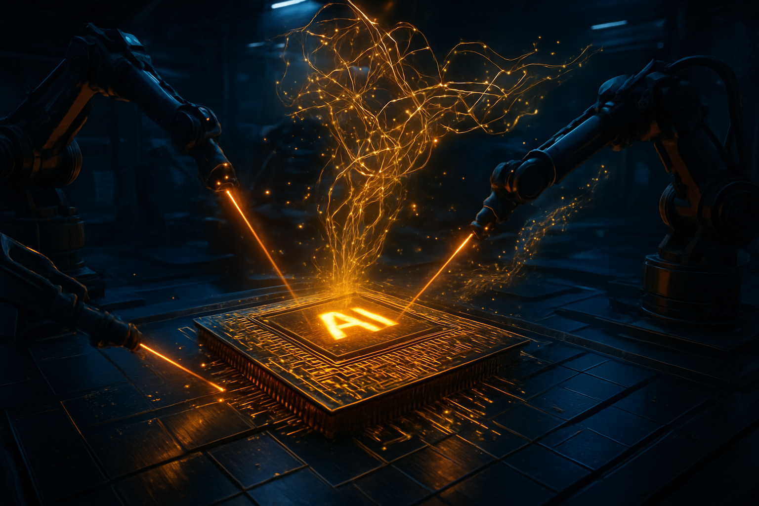
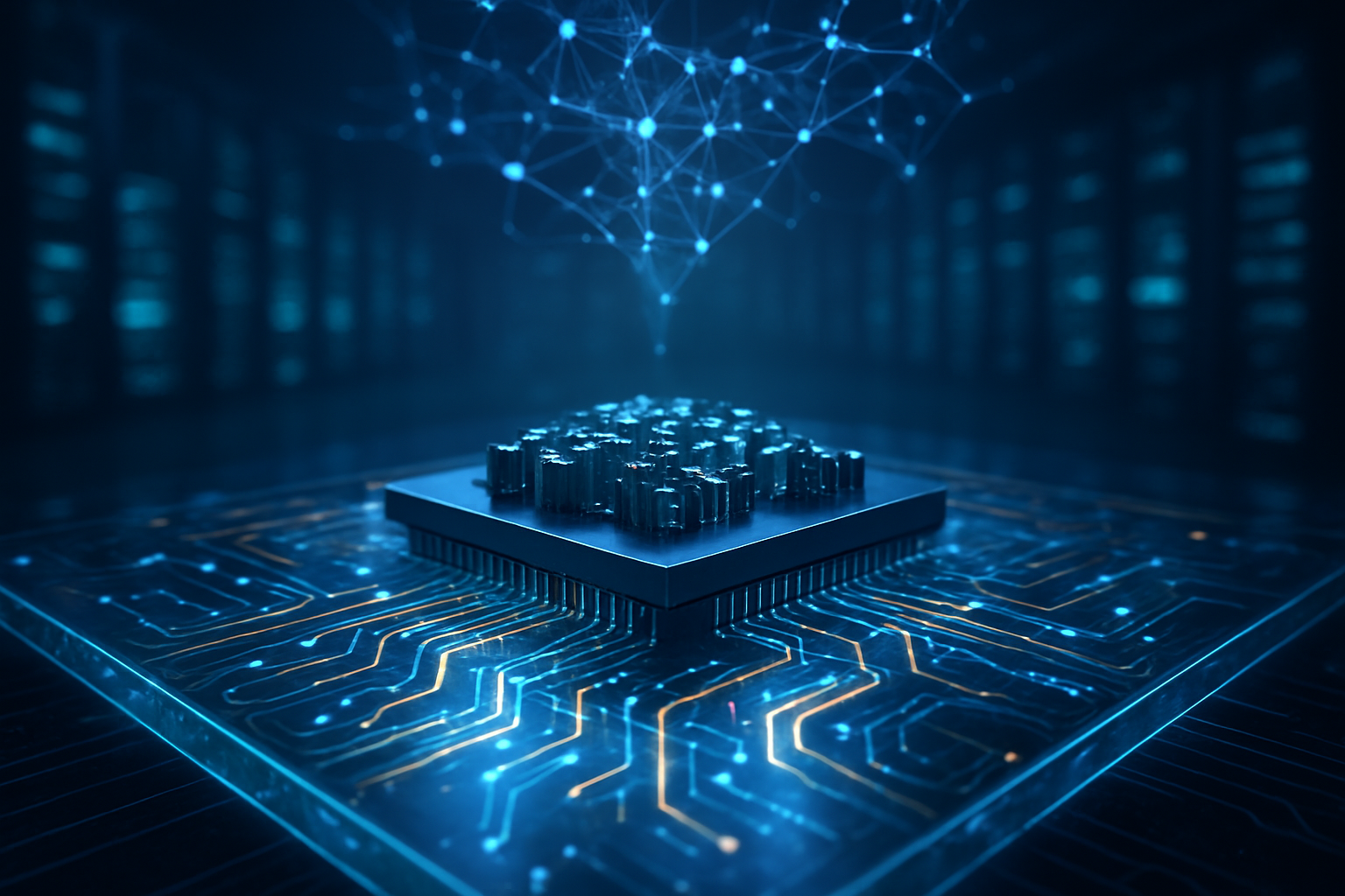
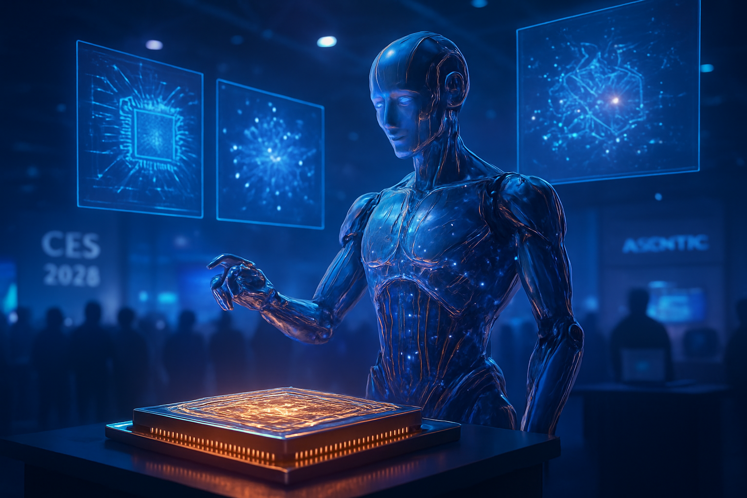
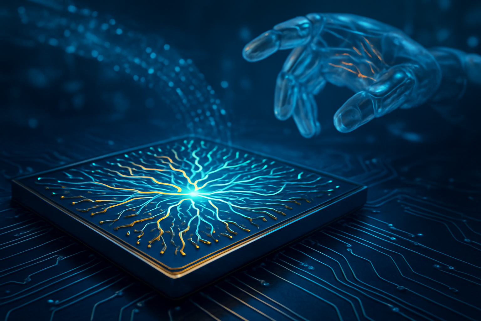
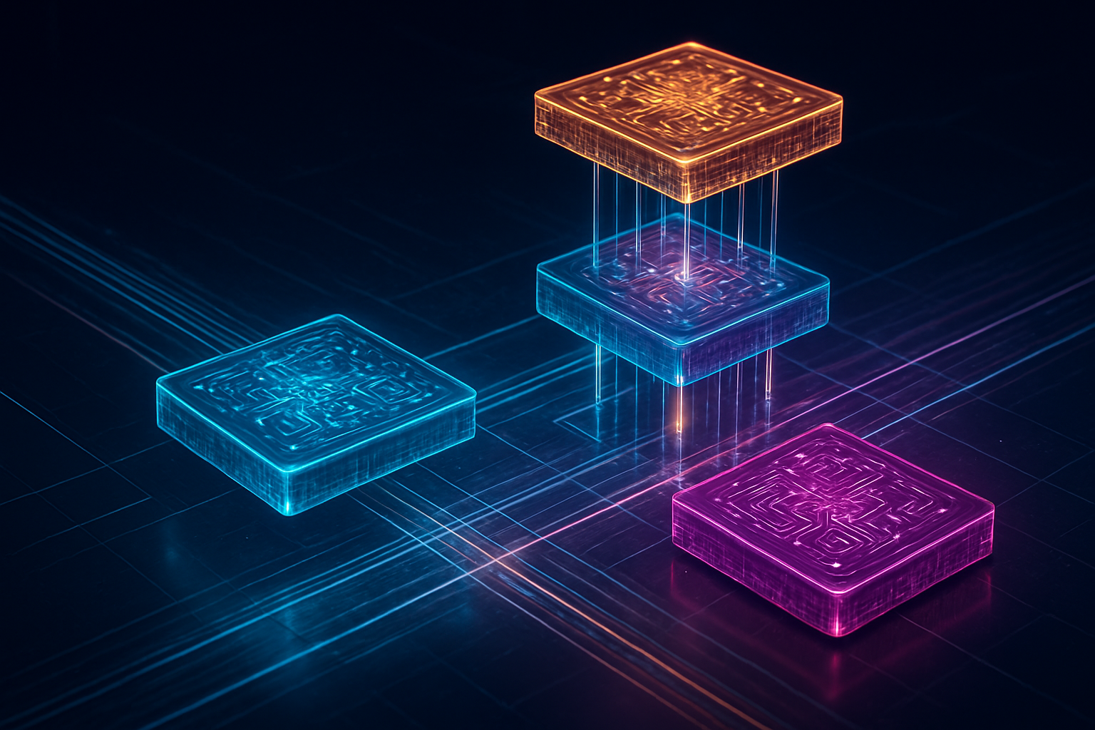
    As of January 22, 2026, the semiconductor industry has reached a definitive turning point: the era of the monolithic processor—a single, massive slab of silicon—is officially coming to a close. In its place, the Universal Chiplet Interconnect Express (UCIe) standard has emerged as the architectural backbone of the next generation of artificial intelligence hardware. By providing a standardized, high-speed "language" for different chips to talk to one another, UCIe is enabling a "Silicon Lego" approach that allows technology giants to mix and match specialized components, drastically accelerating the development of AI accelerators and high-performance computing (HPC) systems.

    This shift is more than a technical upgrade; it represents a fundamental change in how the industry builds the brains of AI. As the demand for larger large language models (LLMs) and complex multi-modal AI continues to outpace the limits of traditional physics, the ability to combine a cutting-edge 2nm compute die from one vendor with a specialized networking tile or high-capacity memory stack from another has become the only viable path forward. However, this modular future is not without its growing pains, as engineers grapple with the physical limitations of "warpage" and the unprecedented complexity of integrating disparate silicon architectures into a single, cohesive package.

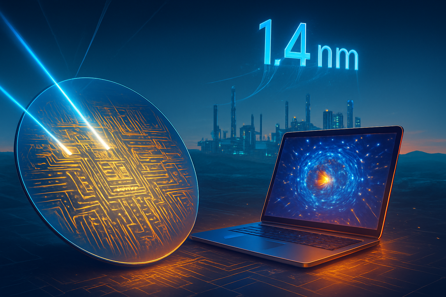
    Breaking the 2nm Barrier: The Technical Foundation of UCIe 2.0 and 3.0

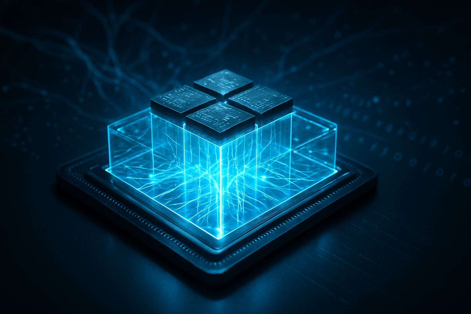
    The technical landscape in early 2026 is dominated by the implementation of the UCIe 2.0 specification, which has successfully moved chiplet communication into the third dimension. While earlier versions focused on 2D and 2.5D integration, UCIe 2.0 was specifically designed to support "3D-native" architectures. This involves hybrid bonding with bump pitches as small as one micron, allowing chiplets to be stacked directly on top of one another with minimal signal loss. This capability is critical for the low-latency requirements of 2026’s AI workloads, which require massive data transfers between logic and memory at speeds previously impossible with traditional interconnects.

    Unlike previous proprietary links—such as early versions of NVLink or Infinity Fabric—UCIe provides a standardized protocol stack that includes a Physical Layer, a Die-to-Die Adapter, and a Protocol Layer that can map directly to CXL or PCIe. The current implementation of UCIe 2.0 facilitates unprecedented power efficiency, delivering data at a fraction of the energy cost of traditional off-chip communication. Furthermore, the industry is already seeing the first pilot designs for UCIe 3.0, which was announced in late 2025. This upcoming iteration promises to double bandwidth again to 64 GT/s per pin, incorporating "runtime recalibration" to adjust power and signal integrity on the fly as thermal conditions change within the package.

    The reaction from the industry has been one of cautious triumph. While experts at major research hubs like IMEC and the IEEE have lauded the standard for finally breaking the "reticle limit"—the physical size limit of a single silicon wafer exposure—they also warn that we are entering an era of "system-in-package" (SiP) complexity. The challenge has shifted from "how do we make a faster transistor?" to "how do we manage the traffic between twenty different transistors made by five different companies?"

    The New Power Players: How Tech Giants are Leveraging the Standard

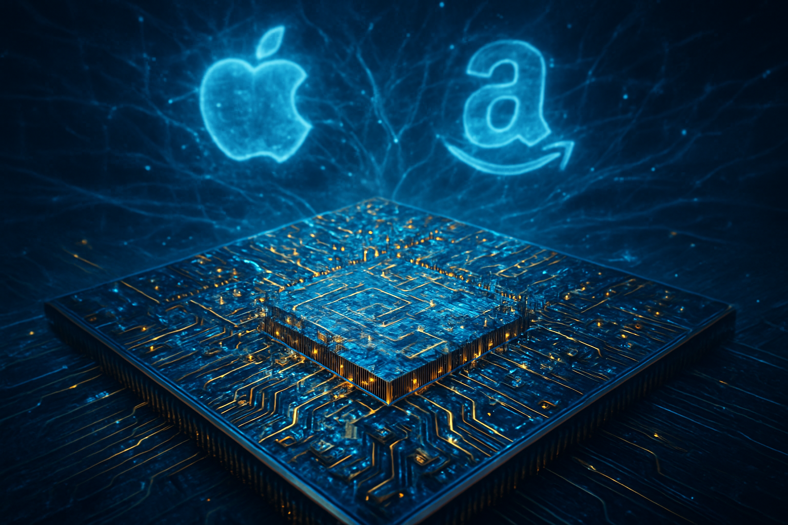
    The adoption of UCIe has sparked a strategic realignment among the world's leading semiconductor firms. Intel Corporation (NASDAQ: INTC) has emerged as a primary beneficiary of this trend through its IDM 2.0 strategy. Intel’s upcoming Xeon 6+ "Clearwater Forest" processors are the flagship example of this new era, utilizing UCIe to connect various compute tiles and I/O dies. By opening its world-class packaging facilities to others, Intel is positioning itself not just as a chipmaker, but as the "foundry of the chiplet era," inviting rivals and partners alike to build their chips on its modular platforms.

    Meanwhile, NVIDIA Corporation (NASDAQ: NVDA) and Advanced Micro Devices, Inc. (NASDAQ: AMD) are locked in a fierce battle for AI supremacy using these modular tools. NVIDIA's newly announced "Rubin" architecture, slated for full rollout throughout 2026, utilizes UCIe 2.0 to integrate HBM4 memory directly atop GPU logic. This 3D stacking, enabled by TSMC’s (NYSE: TSM) advanced SoIC-X platform, allows NVIDIA to pack significantly more performance into a smaller footprint than the previous "Blackwell" generation. AMD, a long-time pioneer of chiplet designs, is using UCIe to allow its hyperscale customers to "drop in" their own custom AI accelerators alongside AMD's EPYC CPU cores, creating a level of hardware customization that was previously reserved for the most expensive boutique designs.

    This development is particularly disruptive for networking-focused firms like Marvell Technology, Inc. (NASDAQ: MRVL) and design-IP leaders like Arm Holdings plc (NASDAQ: ARM). These companies are now licensing "UCIe-ready" chiplet designs that can be slotted into any major cloud provider's custom silicon. This shifts the competitive advantage away from those who can build the largest chip toward those who can design the most efficient, specialized "tile" that fits into the broader UCIe ecosystem.

    The Warpage Wall: Physical Challenges and Global Implications

    Despite the promise of modularity, the industry has hit a significant physical hurdle known as the "Warpage Wall." When multiple chiplets—often manufactured using different processes or materials like Silicon and Gallium Nitride—are bonded together, they react differently to heat. This phenomenon, known as Coefficient of Thermal Expansion (CTE) mismatch, causes the substrate to bow or "warp" during the manufacturing process. As packages grow larger than 55mm to accommodate more AI power, this warpage can lead to "smiling" or "crying" bowing, which snaps the delicate microscopic connections between the chiplets and renders the entire multi-thousand-dollar processor useless.

    This physical reality has significant implications for the broader AI landscape. It has created a new bottleneck in the supply chain: advanced packaging capacity. While many companies can design a chiplet, only a handful—primarily TSMC, Intel, and Samsung Electronics (KRX: 005930)—possess the sophisticated thermal management and bonding technology required to prevent warpage at scale. This concentration of power in packaging facilities has become a geopolitical concern, as nations scramble to secure not just chip manufacturing, but the "advanced assembly" capabilities that allow these chiplets to function.

    Furthermore, the "mix and match" dream faces a legal and business hurdle: the "Known Good Die" (KGD) liability. If a system-in-package containing chiplets from four different vendors fails, the industry is still struggling to determine who is financially responsible. This has led to a market where "modular subsystems" are more common than a truly open marketplace; companies are currently preferring to work in tight-knit groups or "trusted ecosystems" rather than buying random parts off a shelf.

    Future Horizons: Glass Substrates and the Modular AI Frontier

    Looking toward the late 2020s, the next leap in overcoming these integration challenges lies in the transition from organic substrates to glass. Intel and Samsung have already begun demonstrating glass-core substrates that offer exceptional flatness and thermal stability, potentially reducing warpage by 40%. These glass substrates will allow for even larger packages, potentially reaching 100mm x 100mm, which could house entire AI supercomputers on a single interconnected board.

    We also expect to see the rise of "AI-native" chiplets—specialized tiles designed specifically for tasks like sparse matrix multiplication or transformer-specific acceleration—that can be updated independently of the main processor. This would allow a data center to upgrade its "AI engine" chiplet every 12 months without having to replace the more expensive CPU and networking infrastructure, significantly lowering the long-term cost of maintaining cutting-edge AI performance.

    However, experts predict that the biggest challenge will soon shift from hardware to software. As chiplet architectures become more heterogeneous, the industry will need "compiler-aware" hardware that can intelligently route data across the UCIe fabric to minimize latency. The next 18 to 24 months will likely see a surge in software-defined hardware tools that treat the entire SiP as a single, virtualized resource.

    A New Chapter in Silicon History

    The rise of the UCIe standard and the shift toward chiplet-based architectures mark one of the most significant transitions in the history of computing. By moving away from the "one size fits all" monolithic approach, the industry has found a way to continue the spirit of Moore’s Law even as the physical limits of silicon become harder to surmount. The "Silicon Lego" era is no longer a distant vision; it is the current reality of the AI industry as of 2026.

    The significance of this development cannot be overstated. It democratizes high-performance hardware design by allowing smaller players to contribute specialized "tiles" to a global ecosystem, while giving tech giants the tools to build ever-larger AI models. However, the path forward remains littered with physical challenges like multi-chiplet warpage and the logistical hurdles of multi-vendor integration.

    In the coming months, the industry will be watching closely as the first glass-core substrates hit mass production and the "Known Good Die" liability frameworks are tested in the courts and the market. For now, the message is clear: the future of AI is not a single, giant chip—it is a community of specialized chiplets, speaking the same language, working in unison.


    This content is intended for informational purposes only and represents analysis of current AI developments.

    TokenRing AI delivers enterprise-grade solutions for multi-agent AI workflow orchestration, AI-powered development tools, and seamless remote collaboration platforms.
    For more information, visit https://www.tokenring.ai/.

  • The 18A Era Begins: Intel Claims the Transistor Crown at CES 2026 with Panther Lake

    The 18A Era Begins: Intel Claims the Transistor Crown at CES 2026 with Panther Lake

    The Intel Corporation (NASDAQ: INTC) officially inaugurated the "18A Era" this month at CES 2026, launching its highly anticipated Core Ultra Series 3 processors, codenamed "Panther Lake." This launch marks more than just a seasonal hardware refresh; it represents the successful completion of CEO Pat Gelsinger’s audacious "five nodes in four years" (5N4Y) strategy, effectively signaling Intel’s return to the vanguard of semiconductor manufacturing.

    The arrival of Panther Lake is being hailed as the most significant milestone for the Silicon Valley giant in over a decade. By moving into high-volume manufacturing on the Intel 18A node, the company has delivered a product that promises to redefine the "AI PC" through unprecedented power efficiency and a massive leap in local processing capabilities. As of January 22, 2026, the tech industry is witnessing a fundamental shift in the competitive landscape as Intel moves to reclaim the title of the world’s most advanced chipmaker from rivals like TSMC (NYSE: TSM).

    Technical Breakthroughs: RibbonFET, PowerVia, and the 18A Architecture

    The Core Ultra Series 3 is the first consumer platform built on the Intel 18A (1.8nm-class) process, a node that introduces two revolutionary architectural changes: RibbonFET and PowerVia. RibbonFET is Intel’s implementation of Gate-All-Around (GAA) transistors, which replace the aging FinFET structure. This design allows for a multi-channel gate that surrounds the transistor channel on all sides, drastically reducing electrical leakage and allowing for finer control over performance and power consumption.

    Complementing this is PowerVia, Intel’s industry-first backside power delivery system. By moving the power routing to the reverse side of the silicon wafer, Intel has decoupled power delivery from data signaling. This separation solves the "voltage droop" issues that have plagued sub-3nm designs, resulting in a staggering 36% improvement in power efficiency at identical clock speeds compared to previous nodes. The top-tier Panther Lake SKUs feature a hybrid architecture of "Cougar Cove" Performance-cores and "Darkmont" Efficiency-cores, delivering a reported 60% leap in multi-threaded performance over the 2024-era Lunar Lake chips.

    Initial reactions from the AI research community have focused heavily on the integrated NPU 5 (Neural Processing Unit). Panther Lake’s dedicated AI silicon delivers 50 TOPS (Trillions of Operations Per Second) on its own, but when combined with the CPU and the new Xe3 "Celestial" integrated graphics, the total platform AI throughput reaches 180 TOPS. This capacity allows for the local execution of large language models (LLMs) that previously required cloud-based acceleration, a feat that industry experts suggest will fundamentally change how users interact with their operating systems and creative software.

    A Seismic Shift in the Competitive Landscape

    The successful rollout of 18A has immediate and profound implications for the entire semiconductor sector. For years, Advanced Micro Devices (NASDAQ: AMD) and Apple Inc. (NASDAQ: AAPL) enjoyed a manufacturing advantage by leveraging TSMC’s superior nodes. However, with TSMC’s N2 (2nm) process seeing slower-than-expected yields in early 2026, Intel has seized a narrow but critical window of "process leadership." This "leadership" isn't just about Intel’s own chips; it is the cornerstone of the Intel Foundry strategy.

    The market impact is already visible. Industry reports indicate that NVIDIA (NASDAQ: NVDA) has committed nearly $5 billion to reserve capacity on Intel’s 18A lines for its next-generation data center components, seeking to diversify its supply chain away from a total reliance on Taiwan. Meanwhile, AMD's upcoming "Zen 6" architecture is not expected to hit the mobile market in volume until late 2026 or early 2027, giving Intel a significant 9-to-12-month head start in the premium laptop and workstation segments.

    For startups and smaller AI labs, the proliferation of 180-TOPS consumer hardware lowers the barrier to entry for "Edge AI" applications. Developers can now build sophisticated, privacy-centric AI tools that run entirely on a user's laptop, bypassing the high costs and latency of centralized APIs. This shift threatens the dominance of cloud-only AI providers by moving the "intelligence" back to the local device.

    The Geopolitical and Philosophical Significance of 18A

    Beyond benchmarks and market share, the 18A milestone is a victory for the "Silicon Shield" strategy in the West. As the first leading-edge node to be manufactured in significant volumes on U.S. soil, 18A represents a critical step toward rebalancing the global semiconductor supply chain. This development fits into the broader trend of "techno-nationalism," where the ability to manufacture the world's fastest transistors is seen as a matter of national security as much as economic prowess.

    However, the rapid advancement of local AI capabilities also raises concerns. With Panther Lake making high-performance AI accessible to hundreds of millions of consumers, the industry faces renewed questions regarding deepfakes, local data privacy, and the environmental impact of keeping "AI-always-on" hardware in every home. While Intel claims a record 27 hours of battery life for Panther Lake reference designs, the aggregate energy consumption of an AI-saturated PC market remains a topic of debate among sustainability advocates.

    Comparatively, the move to 18A is being likened to the transition from vacuum tubes to integrated circuits. It is a "once-in-a-generation" architectural pivot. While previous nodes focused on incremental shrinks, 18A's combination of backside power and GAA transistors represents a fundamental redesign of how electricity moves through silicon, potentially extending the life of Moore’s Law for another decade.

    The Horizon: From Panther Lake to 14A and Beyond

    Looking ahead, Intel's roadmap does not stop at 18A. The company is already touting the development of the Intel 14A node, which is expected to integrate High-NA EUV (Extreme Ultraviolet) lithography more extensively. Near-term, the focus will shift from consumer laptops to the data center with "Clearwater Forest," a Xeon processor built on 18A that aims to challenge the dominance of ARM-based server chips in the cloud.

    Experts predict that the next two years will see a "Foundry War" as TSMC ramps up its own backside power delivery systems to compete with Intel's early-mover advantage. The primary challenge for Intel now is maintaining these yields as production scales from millions to hundreds of millions of units. Any manufacturing hiccups in the next six months could give rivals an opening to close the gap.

    Furthermore, we expect to see a surge in "Physical AI" applications. With Panther Lake being certified for industrial and robotics use cases at launch, the 18A architecture will likely find its way into autonomous delivery drones, medical imaging devices, and advanced manufacturing bots by the end of 2026.

    A Turnaround Validated: Final Assessment

    The launch of Core Ultra Series 3 at CES 2026 is the ultimate validation of Pat Gelsinger’s "Moonshot" for Intel. By successfully executing five process nodes in four years, the company has transformed itself from a struggling incumbent into a formidable manufacturing powerhouse once again. The 18A node is the physical manifestation of this turnaround—a technological marvel that combines RibbonFET and PowerVia to reclaim the top spot in the semiconductor hierarchy.

    Key takeaways for the industry are clear: Intel is no longer "chasing" the leaders; it is setting the pace. The immediate availability of Panther Lake on January 27, 2026, will be the true test of this new era. Watch for the first wave of third-party benchmarks and the subsequent quarterly earnings from Intel and its foundry customers to see if the "18A Era" translates into the financial resurgence the company has promised.

    For now, the message from CES is undeniable: the race for the next generation of computing has a new frontrunner, and it is powered by 1.8nm silicon.


    This content is intended for informational purposes only and represents analysis of current AI developments.

    TokenRing AI delivers enterprise-grade solutions for multi-agent AI workflow orchestration, AI-powered development tools, and seamless remote collaboration platforms.
    For more information, visit https://www.tokenring.ai/.

  • The Silicon Power Shift: How Intel Secured the ‘Golden Ticket’ in the AI Chip Race

    The Silicon Power Shift: How Intel Secured the ‘Golden Ticket’ in the AI Chip Race

    As the global hunger for generative AI compute continues to outpace supply, the semiconductor landscape has reached a historic inflection point in early 2026. Intel (NASDAQ: INTC) has successfully leveraged its "Golden Ticket" opportunity, transforming from a legacy giant in recovery to a pivotal manufacturing partner for the world’s most advanced AI architects. In a move that has sent shockwaves through the industry, NVIDIA (NASDAQ: NVDA), the undisputed king of AI silicon, has reportedly begun shifting significant manufacturing and packaging orders to Intel Foundry, breaking its near-exclusive reliance on the Taiwan Semiconductor Manufacturing Company (NYSE: TSM).

    The catalyst for this shift is a perfect storm of TSMC production bottlenecks and Intel’s technical resurgence. While TSMC’s advanced nodes remain the gold standard, the company has become a victim of its own success, with its Chip-on-Wafer-on-Substrate (CoWoS) packaging capacity sold out through the end of 2026. This supply-side choke point has left AI titans with a stark choice: wait in a multi-quarter queue for TSMC’s limited output or diversify their supply chains. Intel, having finally achieved high-volume manufacturing with its 18A process node, has stepped into the breach, positioning itself as the necessary alternative to stabilize the global AI economy.

    Technical Superiority and the Power of 18A

    The centerpiece of Intel’s comeback is the 18A (1.8nm-class) process node, which officially entered high-volume manufacturing at Intel’s Fab 52 facility in Arizona this month. Surpassing industry expectations, 18A yields are currently reported in the 65% to 75% range, a level of maturity that signals commercial viability for mission-critical AI hardware. Unlike previous nodes, 18A introduces two foundational innovations: RibbonFET (Gate-All-Around transistor architecture) and PowerVia (backside power delivery). PowerVia, in particular, has emerged as Intel's "secret sauce," reducing voltage droop by up to 30% and significantly improving performance-per-watt—a metric that is now more valuable than raw clock speed in the energy-constrained world of AI data centers.

    Beyond the transistor level, Intel’s advanced packaging capabilities—specifically Foveros and EMIB (Embedded Multi-Die Interconnect Bridge)—have become its most immediate competitive advantage. While TSMC's CoWoS packaging has been the primary bottleneck for NVIDIA’s Blackwell and Rubin architectures, Intel has aggressively expanded its New Mexico packaging facilities, increasing Foveros capacity by 150%. This allows companies like NVIDIA to utilize Intel’s packaging "as a service," even for chips where the silicon wafers were produced elsewhere. Industry experts have noted that Intel’s EMIB-T technology allows for a relatively seamless transition from TSMC’s ecosystem, enabling chip designers to hit 2026 shipment targets that would have been impossible under a TSMC-only strategy.

    The initial reactions from the AI research and hardware communities have been cautiously optimistic. While TSMC still maintains a slight edge in raw transistor density with its N2 node, the consensus is that Intel has closed the "process gap" for the first time in a decade. Technical analysts at several top-tier firms have pointed out that Intel’s lead in glass substrate development—slated for even broader adoption in late 2026—will offer superior thermal stability for the next generation of 3D-stacked superchips, potentially leapfrogging TSMC’s traditional organic material approach.

    A Strategic Realignment for Tech Giants

    The ramifications of Intel’s "Golden Ticket" extend far beyond its own balance sheet, altering the strategic positioning of every major player in the AI space. NVIDIA’s decision to utilize Intel Foundry for its non-flagship networking silicon and specialized H-series variants represents a masterful risk mitigation strategy. By diversifying its foundry partners, NVIDIA can bypass the "TSMC premium"—wafer prices that have climbed by double digits annually—while ensuring a steady flow of hardware to enterprise customers who are less dependent on the absolute cutting-edge performance of the upcoming Rubin R100 flagship.

    NVIDIA is not the only giant making the move; the "Foundry War" of 2026 has seen a flurry of new partnerships. Apple (NASDAQ: AAPL) has reportedly qualified Intel’s 18A node for a subset of its entry-level M-series chips, marking the first time the iPhone maker has moved away from TSMC exclusivity in nearly twenty years. Meanwhile, Microsoft (NASDAQ: MSFT) and Amazon (NASDAQ: AMZN) have solidified their roles as anchor customers, with Microsoft’s Maia AI accelerators and Amazon’s custom AI fabric chips now rolling off Intel’s Arizona production lines. This shift provides these companies with greater bargaining power against TSMC and insulates them from the geopolitical vulnerabilities associated with concentrated production in the Taiwan Strait.

    For startups and specialized AI labs, Intel’s emergence provides a lifeline. During the "Compute Crunch" of 2024 and 2025, smaller players were often crowded out of TSMC’s production schedule by the massive orders from the "Magnificent Seven." Intel’s excess capacity and its eagerness to win market share have created a more democratic landscape, allowing second-tier AI chipmakers and custom ASIC vendors to bring their products to market faster. This disruption is expected to accelerate the development of "Sovereign AI" initiatives, where nations and regional clouds seek to build independent compute stacks on domestic soil.

    The Geopolitical and Economic Landscape

    Intel’s resurgence is inextricably linked to the broader trend of "Silicon Nationalism." In late 2025, the U.S. government effectively nationalized the success of Intel, with the administration taking a 9.9% equity stake in the company as part of a $8.9 billion investment. Combined with the $7.86 billion in direct funding from the CHIPS Act, Intel has gained access to nearly $57 billion in early cash, allowing it to accelerate the construction of massive "Silicon Heartland" hubs in Ohio and Arizona. This unprecedented level of state support has positioned Intel as the sole provider for the "Secure Enclave" program, a $3 billion initiative to ensure that the U.S. military and intelligence agencies have a trusted, domestic source of leading-edge AI silicon.

    This shift marks a departure from the globalization-first era of the early 2000s. The "Golden Ticket" isn't just about manufacturing efficiency; it's about supply chain resilience. As the world moves toward 2027, the semiconductor industry is moving away from a single-choke-point model toward a multi-polar foundry system. While TSMC remains the most profitable entity in the ecosystem, it no longer holds the totalizing influence it once did. The transition mirrors previous industry milestones, such as the rise of fabless design in the 1990s, but with a modern twist: the physical location and political alignment of the fab now matter as much as the nanometer count.

    However, this transition is not without concerns. Critics point out that the heavy government involvement in Intel could lead to market distortions or a "too big to fail" mentality that might stifle long-term innovation. Furthermore, while Intel has captured the "Golden Ticket" for now, the environmental impact of such a massive domestic manufacturing ramp-up—particularly regarding water usage in the American Southwest—remains a point of intense public and regulatory scrutiny.

    The Horizon: 14A and the Road to 2027

    Looking ahead, the next 18 to 24 months will be defined by the race toward the 1.4nm threshold. Intel is already teasing its 14A node, which is expected to enter risk production by early 2027. This next step will lean even more heavily on High-NA EUV (Extreme Ultraviolet) lithography, a technology where Intel has secured an early lead in equipment installation. If Intel can maintain its execution momentum, it could feasibly become the primary manufacturer for the next wave of "Edge AI" devices—smartphones and PCs that require massive on-device inference capabilities with minimal power draw.

    The potential applications for this newfound capacity are vast. We are likely to see an explosion in highly specialized AI ASICs (Application-Specific Integrated Circuits) tailored for robotics, autonomous logistics, and real-time medical diagnostics. These chips require the advanced 3D-packaging that Intel has pioneered but at volumes that TSMC previously could not accommodate. Experts predict that by 2028, the "Intel-Inside" brand will be revitalized, not just as a processor in a laptop, but as the foundational infrastructure for the autonomous economy.

    The immediate challenge for Intel remains scaling. Transitioning from successful "High-Volume Manufacturing" to "Global Dominance" requires a flawless logistical execution that the company has struggled with in the past. To maintain its "Golden Ticket," Intel must prove to customers like Broadcom (NASDAQ: AVGO) and AMD (NASDAQ: AMD) that it can sustain high yields consistently across multiple geographic sites, even as it navigates the complexities of integrated device manufacturing and third-party foundry services.

    A New Era of Semiconductor Resilience

    The events of early 2026 have rewritten the playbook for the AI industry. Intel’s ability to capitalize on TSMC’s bottlenecks has not only saved its own business but has provided a critical safety valve for the entire technology sector. The "Golden Ticket" opportunity has successfully turned the "chip famine" into a competitive market, fostering innovation and reducing the systemic risk of a single-source supply chain.

    In the history of AI, this period will likely be remembered as the "Great Re-Invention" of the American foundry. Intel’s transformation into a viable, leading-edge alternative for companies like NVIDIA and Apple is a testament to the power of strategic technical pivots combined with aggressive industrial policy. As the first 18A-powered AI servers begin to ship to data centers this quarter, the industry's eyes will be fixed on the performance data.

    In the coming weeks and months, watchers should look for the first formal performance benchmarks of NVIDIA-Intel hybrid products and any further shifts in Apple’s long-term silicon roadmap. While the "Foundry War" is far from over, for the first time in decades, the competition is truly global, and the stakes have never been higher.


    This content is intended for informational purposes only and represents analysis of current AI developments.

    TokenRing AI delivers enterprise-grade solutions for multi-agent AI workflow orchestration, AI-powered development tools, and seamless remote collaboration platforms. For more information, visit https://www.tokenring.ai/.

  • Silicon Sovereignty: Apple and Amazon Anchor Intel’s 18A Era

    Silicon Sovereignty: Apple and Amazon Anchor Intel’s 18A Era

    The global semiconductor landscape has reached a historic inflection point as reports emerge that Apple Inc. (NASDAQ: AAPL) and Amazon.com, Inc. (NASDAQ: AMZN) have officially solidified their positions as anchor customers for Intel Corporation’s (NASDAQ: INTC) 18A (1.8nm-class) foundry services. This development marks the most significant validation to date of Intel’s ambitious "IDM 2.0" strategy, positioning the American chipmaker as a formidable rival to the Taiwan Semiconductor Manufacturing Company (NYSE: TSM), commonly known as TSMC.

    For the first time in over a decade, the leading edge of chip manufacturing is no longer the exclusive domain of Asian foundries. Amazon’s commitment involves a multi-billion-dollar expansion to produce custom AI fabric chips, while Apple has reportedly qualified the 18A process for its next generation of entry-level M-series processors. These partnerships represent more than just business contracts; they signify a strategic realignment of the world’s most powerful tech giants toward a more diversified and geographically resilient supply chain.

    The 18A Breakthrough: PowerVia and RibbonFET Redefine Efficiency

    Technically, Intel’s 18A node is not merely an incremental upgrade but a radical shift in transistor architecture. It introduces two industry-first technologies: RibbonFET and PowerVia. RibbonFET is Intel’s implementation of Gate-All-Around (GAA) transistors, which provide better electrostatic control and higher drive current at lower voltages. However, the real "secret sauce" is PowerVia—a backside power delivery system that separates power routing from signal routing. By moving power lines to the back of the wafer, Intel has eliminated the "congestion" that typically plagues advanced nodes, leading to a projected 10-15% improvement in performance-per-watt over existing technologies.

    As of January 2026, Intel’s 18A has entered high-volume manufacturing (HVM) at its Fab 52 facility in Arizona. While TSMC’s N2 node currently maintains a slight lead in raw transistor density, Intel’s 18A has claimed the performance crown for the first half of 2026 due to its early adoption of backside power delivery—a feature TSMC is not expected to integrate until its N2P or A16 nodes later this year. Initial reactions from the AI research community have been overwhelmingly positive, with experts noting that the 18A process is uniquely suited for the high-bandwidth, low-latency requirements of modern AI accelerators.

    A New Global Order: The Strategic Realignment of Big Tech

    The implications for the competitive landscape are profound. Amazon’s decision to fab its "AI fabric chip" on 18A is a direct play to scale its internal AI infrastructure. These chips are designed to optimize NeuronLink technology, the high-speed interconnect used in Amazon’s Trainium and Inferentia AI chips. By bringing this production to Intel’s domestic foundries, Amazon (NASDAQ: AMZN) reduces its reliance on the strained global supply chain while gaining access to Intel’s advanced packaging capabilities.

    Apple’s move is arguably more seismic. Long considered TSMC’s most loyal and important customer, Apple (NASDAQ: AAPL) is reportedly using Intel’s 18AP (a performance-enhanced version of 18A) for its entry-level M-series SoCs found in the MacBook Air and iPad Pro. While Apple’s flagship iPhone chips remain on TSMC’s roadmap for now, the diversification into Intel Foundry suggests a "Taiwan+1" strategy designed to hedge against geopolitical risks in the Taiwan Strait. This move puts immense pressure on TSMC (NYSE: TSM) to maintain its pricing power and technological lead, while offering Intel the "VIP" validation it needs to attract other major fabless firms like Nvidia (NASDAQ: NVDA) and Advanced Micro Devices, Inc. (NASDAQ: AMD).

    De-risking the Digital Frontier: Geopolitics and the AI Hardware Boom

    The broader significance of these agreements lies in the concept of silicon sovereignty. Supported by the U.S. CHIPS and Science Act, Intel has positioned itself as a "National Strategic Asset." The successful ramp-up of 18A in Arizona provides the United States with a domestic 2nm-class manufacturing capability, a milestone that seemed impossible during Intel’s manufacturing stumbles in the late 2010s. This shift is occurring just as the "AI PC" market explodes; by late 2026, half of all PC shipments are expected to feature high-TOPS NPUs capable of running generative AI models locally.

    Furthermore, this development challenges the status of Samsung Electronics (KRX: 005930), which has struggled with yield issues on its own 2nm GAA process. With Intel proving its ability to hit a 60-70% yield threshold on 18A, the market is effectively consolidating into a duopoly at the leading edge. The move toward onshoring and domestic manufacturing is no longer a political talking point but a commercial reality, as tech giants prioritize supply chain certainty over marginal cost savings.

    The Road to 14A: What’s Next for the Silicon Renaissance

    Looking ahead, the industry is already shifting its focus to the next frontier: Intel’s 14A node. Expected to enter production by 2027, 14A will be the world’s first process to utilize High-NA EUV (Extreme Ultraviolet) lithography at scale. Analyst reports suggest that Apple is already eyeing the 14A node for its 2028 iPhone "A22" chips, which could represent a total migration of Apple’s most valuable silicon to American soil.

    Near-term challenges remain, however. Intel must prove it can manage the massive volume requirements of both Apple and Amazon simultaneously without compromising the yields of its internal products, such as the newly launched Panther Lake processors. Additionally, the integration of advanced packaging—specifically Intel’s Foveros technology—will be critical for the multi-die architectures that Amazon’s AI fabric chips require.

    A Turning Point in Semiconductor History

    The reports of Apple and Amazon joining Intel 18A represent the most significant shift in the semiconductor industry in twenty years. It marks the end of the era where leading-edge manufacturing was synonymous with a single geographic region and a single company. Intel has successfully navigated its "Five Nodes in Four Years" roadmap, culminating in a product that has attracted the world’s most demanding silicon customers.

    As we move through 2026, the key metrics to watch will be the final yield rates of the 18A process and the performance benchmarks of the first consumer products powered by these chips. If Intel can deliver on its promises, the 18A era will be remembered as the moment the silicon balance of power shifted back to the West, fueled by the insatiable demand for AI and the strategic necessity of supply chain resilience.


    This content is intended for informational purposes only and represents analysis of current AI developments.

    TokenRing AI delivers enterprise-grade solutions for multi-agent AI workflow orchestration, AI-powered development tools, and seamless remote collaboration platforms.
    For more information, visit https://www.tokenring.ai/.

  • The Dawn of the Glass Age: How Glass Substrates and 3D Transistors Are Shattering the AI Performance Ceiling

    The Dawn of the Glass Age: How Glass Substrates and 3D Transistors Are Shattering the AI Performance Ceiling

    CHANDLER, AZ – In a move that marks the most significant architectural shift in semiconductor manufacturing in over a decade, the industry has officially transitioned into what experts are calling the "Glass Age." As of January 21, 2026, the transition from traditional organic substrates to glass-core technology, coupled with the arrival of the first circuit-ready 3D Complementary Field-Effect Transistors (CFET), has effectively dismantled the physical barriers that threatened to stall the progress of generative AI.

    This development is not merely an incremental upgrade; it is a foundational reset. By replacing the resin-based materials that have housed chips for forty years with ultra-flat, thermally stable glass, manufacturers are now able to build "super-packages" of unprecedented scale. These advancements arrive just in time to power the next generation of trillion-parameter AI models, which have outgrown the electrical and thermal limits of 2024-era hardware.

    Shattering the "Warpage Wall": The Tech Behind the Transition

    The technical shift centers on the transition from Ajinomoto Build-up Film (ABF) organic substrates to glass-core substrates. For years, the industry struggled with the "warpage wall"—a phenomenon where the heat generated by massive AI chips caused traditional organic substrates to expand and contract at different rates than the silicon they supported, leading to microscopic cracks and connection failures. Glass, by contrast, possesses a Coefficient of Thermal Expansion (CTE) that nearly matches silicon. This allows companies like Intel (NASDAQ: INTC) and Samsung (OTC: SSNLF) to manufacture packages exceeding 100mm x 100mm, integrating dozens of chiplets and HBM4 (High Bandwidth Memory) stacks into a single, cohesive unit.

    Beyond the substrate, the industry has reached a milestone in transistor architecture with the successful demonstration of the first fully functional 101-stage monolithic CFET Ring Oscillator by TSMC (NYSE: TSM). While the previous Gate-All-Around (GAA) nanosheets allowed for greater control over current, CFET takes scaling into the third dimension by vertically stacking n-type and p-type transistors directly on top of one another. This 3D stacking effectively halves the footprint of logic gates, allowing for a 10x increase in interconnect density through the use of Through-Glass Vias (TGVs). These TGVs enable microscopic electrical paths with pitches of less than 10μm, reducing signal loss by 40% compared to traditional organic routing.

    The New Hierarchy: Intel, Samsung, and the Race for HVM

    The competitive landscape of the semiconductor industry has been radically reordered by this transition. Intel (NASDAQ: INTC) has seized an early lead, announcing this month that its facility in Chandler, Arizona, has officially moved glass substrate technology into High-Volume Manufacturing (HVM). Its first commercial product utilizing this technology, the Xeon 6+ "Clearwater Forest," is already shipping to major cloud providers. Intel’s early move positions its Foundry Services as a critical partner for US-based AI giants like Amazon (NASDAQ: AMZN) and Google (NASDAQ: GOOGL), who are seeking to insulate their supply chains from geopolitical volatility.

    Samsung (KRX: 005930), meanwhile, has leveraged its "Triple Alliance"—a collaboration between its Foundry, Display, and Electro-Mechanics divisions—to fast-track its "Dream Substrate" program. Samsung is targeting the second half of 2026 for mass production, specifically aiming for the high-end AI ASIC market. Not to be outdone, TSMC (NYSE: TSM) has begun sampling its Chip-on-Panel-on-Substrate (CoPoS) glass solution for Nvidia (NASDAQ: NVDA). Nvidia’s newly announced "Vera Rubin" R100 platform is expected to be the primary beneficiary of this tech, aiming for a 5x boost in AI inference capabilities by utilizing the superior signal integrity of glass to manage its staggering 19.6 TB/s HBM4 bandwidth.

    Geopolitics and Sustainability: The High Stakes of High Tech

    The shift to glass has created a new geopolitical "moat" around the Western-Korean semiconductor axis. As the manufacturing of these advanced substrates requires high-precision equipment and specialized raw materials—such as the low-CTE glass cloth produced almost exclusively by Japan’s Nitto Boseki—a new bottleneck has emerged. US and South Korean firms have secured long-term contracts for these materials, creating a 12-to-18-month lead over Chinese rivals like BOE and Visionox, who are currently struggling with high-volume yields. This technological gap has become a cornerstone of the US strategy to maintain leadership in high-performance computing (HPC).

    From a sustainability perspective, the move is a double-edged sword. The manufacturing of glass substrates is more energy-intensive than organic ones, requiring high-temperature furnaces and complex water-reclamation protocols. However, the operational benefits are transformative. By reducing power loss during data movement by 50%, glass-packaged chips are significantly more energy-efficient once deployed in data centers. In an era where AI power consumption is measured in gigawatts, the "Performance per Watt" advantage of glass is increasingly seen as the only viable path to sustainable AI scaling.

    Future Horizons: From Electrical to Optical

    Looking toward 2027 and beyond, the transition to glass substrates paves the way for the "holy grail" of chip design: integrated co-packaged optics (CPO). Because glass is transparent and ultra-flat, it serves as a perfect medium for routing light instead of electricity. Experts predict that within the next 24 months, we will see the first AI chips that use optical interconnects directly on the glass substrate, virtually eliminating the "power wall" that currently limits how fast data can move between the processor and memory.

    However, challenges remain. The brittleness of glass continues to pose yield risks, with current manufacturing lines reporting breakage rates roughly 5-10% higher than organic counterparts. Additionally, the industry must develop new standardized testing protocols for 3D-stacked CFET architectures, as traditional "probing" methods are difficult to apply to vertically stacked transistors. Industry consortiums are currently working to harmonize these standards to ensure that the "Glass Age" doesn't suffer from a lack of interoperability.

    A Decisive Moment in AI History

    The transition to glass substrates and 3D transistors marks a definitive moment in the history of computing. By moving beyond the physical limitations of 20th-century materials, the semiconductor industry has provided AI developers with the "infinite" canvas required to build the first truly agentic, world-scale AI systems. The ability to stitch together dozens of chiplets into a single, thermally stable package means that the 1,000-watt AI accelerator is no longer a thermal nightmare, but a manageable reality.

    As we move into the spring of 2026, all eyes will be on the yield rates of Intel's Arizona lines and the first performance benchmarks of AMD’s (NASDAQ: AMD) Instinct MI400 series, which is slated to utilize glass substrates from merchant supplier Absolics later this year. The "Silicon Valley" of the future may very well be built on a foundation of glass, and the companies that master this transition first will likely dictate the pace of AI innovation for the remainder of the decade.


    This content is intended for informational purposes only and represents analysis of current AI developments.

    TokenRing AI delivers enterprise-grade solutions for multi-agent AI workflow orchestration, AI-powered development tools, and seamless remote collaboration platforms.
    For more information, visit https://www.tokenring.ai/.

  • The Era of Light: Silicon Photonics Shatters the ‘Memory Wall’ as AI Scaling Hits the Copper Ceiling

    The Era of Light: Silicon Photonics Shatters the ‘Memory Wall’ as AI Scaling Hits the Copper Ceiling

    As of January 2026, the artificial intelligence industry has officially entered what architects are calling the "Era of Light." For years, the rapid advancement of Large Language Models (LLMs) was threatened by two looming physical barriers: the "memory wall"—the bottleneck where data cannot move fast enough between processors and memory—and the "copper wall," where traditional electrical wiring began to fail under the sheer volume of data required for trillion-parameter models. This week, a series of breakthroughs in Silicon Photonics (SiPh) and Optical I/O (Input/Output) have signaled the end of these constraints, effectively decoupling the physical location of hardware from its computational performance.

    The shift is represented most poignantly by the mass commercialization of Co-Packaged Optics (CPO) and optical memory pooling. By replacing copper wires with laser-driven light signals directly on the chip package, industry giants have managed to reduce interconnect power consumption by over 70% while simultaneously increasing bandwidth density by a factor of ten. This transition is not merely an incremental upgrade; it is a fundamental architectural reset that allows data centers to operate as a single, massive "planet-scale" computer rather than a collection of isolated server racks.

    The Technical Breakdown: Moving Beyond Electrons

    The core of this advancement lies in the transition from pluggable optics to integrated optical engines. In the previous era, data was moved via copper traces on a circuit board to an optical transceiver at the edge of the rack. At the current 224 Gbps signaling speeds, copper loses its integrity after less than a meter, and the heat generated by electrical resistance becomes unmanageable. The latest technical specifications for January 2026 show that Optical I/O, pioneered by firms like Ayar Labs and Celestial AI (recently acquired by Marvell (NASDAQ: MRVL)), has achieved energy efficiencies of 2.4 to 5 picojoules per bit (pJ/bit), a staggering improvement over the 12–15 pJ/bit required by 2024-era copper systems.

    Central to this breakthrough is the "Optical Compute Interconnect" (OCI) chiplet. Intel (NASDAQ: INTC) has begun high-volume manufacturing of these chiplets using its new glass substrate technology in Arizona. These glass substrates provide the thermal and physical stability necessary to bond photonic engines directly to high-power AI accelerators. Unlike previous approaches that relied on external lasers, these new systems feature "multi-wavelength" light sources that can carry terabits of data across a single fiber-optic strand with latencies below 10 nanoseconds.

    Initial reactions from the AI research community have been electric. Dr. Arati Prabhakar, leading a consortium of high-performance computing (HPC) experts, noted that the move to optical fabrics has "effectively dissolved the physical boundaries of the server." By achieving sub-300ns latency for cross-rack communication, researchers can now train models with tens of trillions of parameters across "million-GPU" clusters without the catastrophic performance degradation that previously plagued large-scale distributed training.

    The Market Landscape: A New Hierarchy of Power

    This shift has created clear winners and losers in the semiconductor space. NVIDIA (NASDAQ: NVDA) has solidified its dominance with the unveiling of the Vera Rubin platform. The Rubin architecture utilizes NVLink 6 and the Spectrum-6 Ethernet switch, the latter of which is the world’s first to fully integrate Spectrum-X Ethernet Photonics. By moving to an all-optical backplane, NVIDIA has managed to double GPU-to-GPU bandwidth to 3.6 TB/s while significantly lowering the total cost of ownership for cloud providers by slashing cooling requirements.

    Broadcom (NASDAQ: AVGO) remains the titan of the networking layer, now shipping its Tomahawk 6 "Davisson" switch in massive volumes. This 102.4 Tbps switch utilizes TSMC (NYSE: TSM) "COUPE" (Compact Universal Photonic Engine) technology, which heterogeneously integrates optical engines and silicon into a single 3D package. This integration has forced traditional networking companies like Cisco (NASDAQ: CSCO) to pivot aggressively toward silicon-proven optical solutions to avoid being marginalized in the AI-native data center.

    The strategic advantage now belongs to those who control the "Scale-Up" fabric—the interconnects that allow thousands of GPUs to work as one. Marvell’s (NASDAQ: MRVL) acquisition of Celestial AI has positioned them as the primary provider of optical memory appliances. These devices provide up to 33TB of shared HBM4 capacity, allowing any GPU in a data center to access a massive pool of memory as if it were on its own local bus. This "disaggregated" approach is a nightmare for legacy server manufacturers but a boon for hyperscalers like Amazon and Google, who are desperate to maximize the utilization of their expensive silicon.

    Wider Significance: Environmental and Architectural Rebirth

    The rise of Silicon Photonics is about more than just speed; it is the industry’s most viable answer to the environmental crisis of AI energy consumption. Data centers were on a trajectory to consume an unsustainable percentage of global electricity by 2030. However, the 70% reduction in interconnect power offered by optical I/O provides a necessary "reset" for the industry’s carbon footprint. By moving data with light instead of heat-generating electrons, the energy required for data movement—which once accounted for 30% of a cluster’s power—has been drastically curtailed.

    Historically, this milestone is being compared to the transition from vacuum tubes to transistors. Just as the transistor allowed for a scale of complexity that was previously impossible, Silicon Photonics allows for a scale of data movement that finally matches the computational potential of modern neural networks. The "Memory Wall," a term coined in the mid-1990s, has been the single greatest hurdle in computer architecture for thirty years. To see it finally "shattered" by light-based memory pooling is a moment that will likely define the next decade of computing history.

    However, concerns remain regarding the "Yield Wars." The 3D stacking of silicon, lasers, and optical fibers is incredibly complex. As TSMC, Samsung (KOSPI: 005930), and Intel compete for dominance in these advanced packaging techniques, any slip in manufacturing yields could cause massive supply chain disruptions for the world's most critical AI infrastructure.

    The Road Ahead: Planet-Scale Compute and Beyond

    In the near term, we expect to see the "Optical-to-the-XPU" movement accelerate. Within the next 18 to 24 months, we anticipate the release of AI chips that have no electrical I/O whatsoever, relying entirely on fiber optic connections for both power delivery and data. This will enable "cold racks," where high-density compute can be submerged in dielectric fluid or specialized cooling environments without the interference caused by traditional copper cabling.

    Long-term, the implications for AI applications are profound. With the memory wall removed, we are likely to see a surge in "long-context" AI models that can process entire libraries of data in their active memory. Use cases in drug discovery, climate modeling, and real-time global economic simulation—which require massive, shared datasets—will become feasible for the first time. The challenge now shifts from moving the data to managing the sheer scale of information that can be accessed at light speed.

    Experts predict that the next major hurdle will be "Optical Computing" itself—using light not just to move data, but to perform the actual matrix multiplications required for AI. While still in the early research phases, the success of Silicon Photonics in I/O has proven that the industry is ready to embrace photonics as the primary medium of the information age.

    Conclusion: The Light at the End of the Tunnel

    The emergence of Silicon Photonics and Optical I/O represents a landmark achievement in the history of technology. By overcoming the twin barriers of the memory wall and the copper wall, the semiconductor industry has cleared the path for the next generation of artificial intelligence. Key takeaways include the dramatic shift toward energy-efficient, high-bandwidth optical fabrics and the rise of memory pooling as a standard for AI infrastructure.

    As we look toward the coming weeks and months, the focus will shift from these high-level announcements to the grueling reality of manufacturing scale. Investors and engineers alike should watch the quarterly yield reports from major foundries and the deployment rates of the first "Vera Rubin" clusters. The era of the "Copper Data Center" is ending, and in its place, a faster, cooler, and more capable future is being built on a foundation of light.


    This content is intended for informational purposes only and represents analysis of current AI developments.

    TokenRing AI delivers enterprise-grade solutions for multi-agent AI workflow orchestration, AI-powered development tools, and seamless remote collaboration platforms.
    For more information, visit https://www.tokenring.ai/.

  • The Dawn of the Physical AI Era: Silicon Titans Redefine CES 2026

    The Dawn of the Physical AI Era: Silicon Titans Redefine CES 2026

    The recently concluded CES 2026 in Las Vegas will be remembered as the moment the artificial intelligence revolution stepped out of the chat box and into the physical world. Officially heralded as the "Year of Physical AI," the event marked a historic pivot from the generative text and image models of 2024–2025 toward embodied systems that can perceive, reason, and act within our three-dimensional environment. This shift was underscored by a massive coordinated push from the world’s leading semiconductor manufacturers, who unveiled a new generation of "Physical AI" processors designed to power everything from "Agentic PCs" to fully autonomous humanoid robots.

    The significance of this year’s show lies in the maturation of edge computing. For the first time, the industry demonstrated that the massive compute power required for complex reasoning no longer needs to reside exclusively in the cloud. With the launch of ultra-high-performance NPUs (Neural Processing Units) from the industry's "Four Horsemen"—Nvidia, Intel, AMD, and Qualcomm—the promise of low-latency, private, and physically capable AI has finally moved from research prototypes to mass-market production.

    The Silicon War: Specs of the 'Four Horsemen'

    The technological centerpiece of CES 2026 was the "four-way war" in AI silicon. Nvidia (NASDAQ:NVDA) set the pace early by putting its "Rubin" architecture into full production. CEO Jensen Huang declared a "ChatGPT moment for robotics" as he unveiled the Jetson T4000, a Blackwell-powered module delivering a staggering 1,200 FP4 TFLOPS. This processor is specifically designed to be the "brain" of humanoid robots, supported by Project GR00T and Cosmos, an "open world foundation model" that allows machines to learn motor tasks from video data rather than manual programming.

    Not to be outdone, Intel (NASDAQ:INTC) utilized the event to showcase the success of its turnaround strategy with the official launch of Panther Lake (Core Ultra Series 3). Manufactured on the cutting-edge Intel 18A process node, the chip features the new NPU 5, which delivers 50 TOPS locally. Intel’s focus is the "Agentic AI PC"—a machine capable of managing a user’s entire digital life and local file processing autonomously. Meanwhile, Qualcomm (NASDAQ:QCOM) flexed its efficiency muscles with the Snapdragon X2 Elite Extreme, boasting an 18-core Oryon 3 CPU and an 80 TOPS NPU. Qualcomm also introduced the Dragonwing IQ10, a dedicated platform for robotics that emphasizes power-per-watt, enabling longer battery life for mobile humanoids like the Vinmotion Motion 2.

    AMD (NASDAQ:AMD) rounded out the quartet by bridging the gap between the data center and the desktop. Their new Ryzen AI "Gorgon Point" series features an expanded matrix engine and the first native support for "Copilot+ Desktop" high-performance workloads. AMD also teased its Helios platform, a rack-scale solution powered by Zen 6 EPYC "Venice" processors, intended to train the very physical world models that the smaller Ryzen chips execute at the edge. Industry experts have noted that while previous years focused on software breakthroughs, 2026 is defined by the hardware's ability to handle "multimodal reasoning"—the ability for a device to see an object, understand its physical properties, and decide how to interact with it in real-time.

    Market Maneuvers: From Cloud Dominance to Edge Supremacy

    This shift toward Physical AI is fundamentally reshaping the competitive landscape of the tech industry. For years, the AI narrative was dominated by cloud providers and LLM developers. However, CES 2026 proved that the "edge"—the devices we carry and the robots that work alongside us—is the new battleground for strategic advantage. Nvidia is positioning itself as the "Infrastructure King," providing not just the chips but the entire software stack (Omniverse and Isaac) needed to simulate and train physical entities. By owning the simulation environment, Nvidia seeks to make its hardware the indispensable foundation for every robotics startup.

    In contrast, Qualcomm and Intel are targeting the "volume market." Qualcomm is leveraging its heritage in mobile connectivity to dominate "connected robotics," where 5G and 6G integration are vital for warehouse automation and consumer bots. Intel, through its 18A manufacturing breakthrough, is attempting to reclaim the crown of the "PC Brain" by making AI features so deeply integrated into the OS that a cloud connection becomes optional. Startups like Boston Dynamics (backed by Hyundai and Google DeepMind) and Vinmotion are the primary beneficiaries of this rivalry, as the sudden abundance of high-performance, low-power silicon allows them to transition from experimental models to production-ready units capable of "human-level" dexterity.

    The competitive implications extend beyond silicon. Tech giants are now forced to choose between "walled garden" AI ecosystems or open-source Physical AI frameworks. The move toward local processing also threatens the dominance of current subscription-based AI models; if a user’s Intel-powered laptop or Qualcomm-powered robot can perform complex reasoning locally, the strategic advantage of centralized AI labs like OpenAI or Anthropic could begin to erode in favor of hardware-software integrated giants.

    The Wider Significance: When AI Gets a Body

    The transition from "Digital AI" to "Physical AI" represents a profound milestone in human-computer interaction. For the first time, the "hallucinations" that plagued early generative AI have moved from being a nuisance in text to a safety critical engineering challenge. At CES 2026, panels featuring leaders from Siemens and Mercedes-Benz emphasized that "Physical AI" requires "error intolerance." A robot navigating a crowded home or a factory floor cannot afford a single reasoning error, leading to the introduction of "safety-grade" silicon architectures that partition AI logic from critical motor controls.

    This development also brings significant societal concerns to the forefront. As AI becomes embedded in physical infrastructure—from elevators that predict maintenance to autonomous industrial helpers—the question of accountability becomes paramount. Experts at the event raised alarms regarding "invisible AI," where autonomous systems become so pervasive that their decision-making processes are no longer transparent to the humans they serve. The industry is currently racing to establish "document trails" for AI reasoning to ensure that when a physical system fails, the cause can be diagnosed with the same precision as a mechanical failure.

    Comparatively, the 2023 generative AI boom was about "creation," while the 2026 Physical AI breakthrough is about "utility." We are moving away from AI as a toy or a creative partner and toward AI as a functional laborer. This has reignited debates over labor displacement, but with a new twist: the focus is no longer just on white-collar "knowledge work," but on blue-collar tasks in logistics, manufacturing, and elder care.

    Beyond the Horizon: The 2027 Roadmap

    Looking ahead, the momentum generated at CES 2026 shows no signs of slowing. Near-term developments will likely focus on the refinement of "Agentic AI PCs," where the operating system itself becomes a proactive assistant that performs tasks across different applications without user prompting. Long-term, the industry is already looking toward 2027, with Intel teasing its Nova Lake architecture (rumored to feature 52 cores) and AMD preparing its Medusa (Zen 6) chips based on TSMC’s 2nm process. These upcoming iterations aim to bring even more "brain-like" density to consumer hardware.

    The next major challenge for the industry will be the "sim-to-real" gap—the difficulty of taking an AI trained in a virtual simulation and making it function perfectly in the messy, unpredictable real world. Future applications on the horizon include "personalized robotics," where robots are not just general-purpose tools but are fine-tuned to the specific layout and needs of an individual's home. Predictably, experts believe the next 18 months will see a surge in M&A activity as silicon giants move to acquire robotics software startups to complete their "Physical AI" portfolios.

    The Wrap-Up: A Turning Point in Computing History

    CES 2026 has served as a definitive declaration that the "post-chat" era of artificial intelligence has arrived. The key takeaways from the event are clear: the hardware has finally caught up to the software, and the focus of innovation has shifted from virtual outputs to physical actions. The coordinated launches from Nvidia, Intel, AMD, and Qualcomm have provided the foundation for a world where AI is no longer a guest on our screens but a participant in our physical spaces.

    In the history of AI, 2026 will likely be viewed as the year the technology gained its "body." As we look toward the coming months, the industry will be watching closely to see how these new processors perform in real-world deployments and how consumers react to the first wave of truly autonomous "Agentic" devices. The silicon war is far from over, but the battlefield has officially moved into the real world.


    This content is intended for informational purposes only and represents analysis of current AI developments.

    TokenRing AI delivers enterprise-grade solutions for multi-agent AI workflow orchestration, AI-powered development tools, and seamless remote collaboration platforms.
    For more information, visit https://www.tokenring.ai/.

  • Intel Hits 18A Mass Production: Panther Lake Leads the Charge into the 1.4nm Era

    Intel Hits 18A Mass Production: Panther Lake Leads the Charge into the 1.4nm Era

    In a definitive moment for the American semiconductor industry, Intel (NASDAQ: INTC) has officially transitioned its 18A (1.8nm-class) process node into high-volume manufacturing (HVM). The announcement, made early this month, signals the culmination of CEO Pat Gelsinger’s ambitious "five nodes in four years" roadmap, positioning Intel at the absolute bleeding edge of transistor density and power efficiency. This milestone is punctuated by the overwhelming critical success of the newly launched Panther Lake processors, which have set a new high-water mark for integrated AI performance and power-to-performance ratios in the mobile and desktop segments.

    The shift represents more than just a technical achievement; it marks Intel’s full-scale re-entry into the foundry race as a formidable peer to Taiwan Semiconductor Manufacturing Company (NYSE: TSM). With 18A yields now stabilized above the 60% threshold—a key metric for commercial profitability—Intel is aggressively pivoting its strategic focus toward the upcoming 14A node and the massive "Silicon Heartland" project in Ohio. This pivot underscores a new era of silicon sovereignty and high-performance computing that aims to redefine the AI landscape for the remainder of the decade.

    Technical Mastery: RibbonFET, PowerVia, and the Panther Lake Powerhouse

    The move to 18A introduces two foundational architectural shifts that differentiate it from any previous Intel manufacturing process. The first is RibbonFET, Intel’s implementation of Gate-All-Around (GAA) transistor architecture. By surrounding the channel with the gate on all four sides, RibbonFET significantly reduces current leakage and improves electrostatic control, allowing for higher drive currents at lower voltages. This is paired with PowerVia, the industry’s first large-scale implementation of backside power delivery. By moving power routing to the back of the wafer and leaving the front exclusively for signal routing, Intel has achieved a 15% improvement in clock frequency and a roughly 25% reduction in power consumption, solving long-standing congestion issues in advanced chip design.

    The real-world manifestation of these technologies is the Core Ultra Series 3, codenamed Panther Lake. Debuted at CES 2026 and set for global retail availability on January 27, Panther Lake has already stunned reviewers with its Xe3 "Célere" graphics architecture and the NPU 5. Initial benchmarks show the integrated Arc B390 GPU delivering up to 77% faster gaming performance than its predecessor, effectively rendering mid-range discrete GPUs obsolete for most users. More importantly for the AI era, the system’s total AI throughput reaches a staggering 120 TOPS (Tera Operations Per Second). This is achieved through a massive expansion of the Neural Processing Unit (NPU), which handles complex generative AI tasks locally with a fraction of the power required by previous generations.

    A New Order in the Foundry Ecosystem

    The successful ramp of 18A is sending ripples through the broader tech industry, specifically targeting the dominance of traditional foundry leaders. While Intel remains its own best customer, the 18A node has already attracted high-profile "anchor" clients. Microsoft (NASDAQ: MSFT) and Amazon (NASDAQ: AMZN) have reportedly finalized designs for custom AI accelerators and server chips built on 18A, seeking to reduce their reliance on external providers and optimize their data center overhead. Even more telling are reports that Apple (NASDAQ: AAPL) has qualified 18A for select future components, signaling a potential diversification of its supply chain away from its exclusive reliance on TSMC.

    This development places Intel in a strategic position to disrupt the existing AI silicon market. By offering a domestic, leading-edge alternative for high-performance chips, Intel Foundry is capitalizing on the global push for supply chain resilience. For startups and smaller AI labs, the availability of 18A design kits means faster access to hardware that can run massive localized models. Intel's ability to integrate PowerVia ahead of its competitors gives it a temporary but significant "power-efficiency moat," making it an attractive partner for companies building the next generation of power-hungry AI edge devices and autonomous systems.

    The Geopolitical and Industrial Significance of the 18A Era

    Intel’s achievement is being viewed by many as a successful validation of the U.S. CHIPS and Science Act. With the Department of Commerce maintaining a vested interest in Intel’s success, the 18A milestone is a point of national pride and economic security. In the broader AI landscape, this move ensures that the hardware layer of the AI stack—which has been a significant bottleneck over the last three years—now has a secondary, highly advanced production lane. This reduces the risk of global shortages that previously hampered the deployment of large language models and real-world AI applications.

    However, the path has not been without its concerns. Critics point to the immense capital expenditure required to maintain this pace, which has strained Intel's balance sheet and necessitated a highly disciplined "foundry-first" corporate restructuring. When compared to previous milestones, such as the transition to FinFET or the introduction of EUV (Extreme Ultraviolet) lithography, 18A stands out because of the simultaneous introduction of two radically new technologies (RibbonFET and PowerVia). This "double-jump" was considered high-risk, but its success confirms that Intel has regained its engineering mojo, providing a necessary counterbalance to the concentrated production power in East Asia.

    The Horizon: 14A and the Ohio Silicon Heartland

    With 18A in mass production, Intel’s leadership has already turned their sights toward the 14A (1.4nm-class) node. Slated for production readiness in 2027, 14A will be the first node to fully utilize High-NA EUV lithography at scale. Intel has already begun distributing early Process Design Kits (PDKs) for 14A to key partners, signaling that the company does not intend to let its momentum stall. Experts predict that 14A will offer yet another 15-20% leap in performance-per-watt, further solidifying the AI PC as the standard for enterprise and consumer computing.

    Parallel to this technical roadmap is the massive infrastructure push in New Albany, Ohio. The "Ohio One" project, often called the Silicon Heartland, is making steady progress. While initial production was delayed from 2025, the latest reports from the site indicate that the first two modules (Mod 1 and Mod 2) are on track for physical completion by late 2026. This facility is expected to become the primary hub for Intel’s 14A and beyond, with full-scale chip production anticipated to begin in the 2028 window. The project has become a massive employment engine, with thousands of construction and engineering professionals currently working to finalize the state-of-the-art cleanrooms required for sub-2nm manufacturing.

    Summary of a Landmark Achievement

    Intel's successful mass production of 18A and the triumph of Panther Lake represent a historic pivot for the semiconductor giant. The company has moved from a period of self-described "stagnation" to reclaiming a seat at the head of the manufacturing table. The key takeaways for the industry are clear: Intel’s RibbonFET and PowerVia are the new benchmarks for efficiency, and the "AI PC" has moved from a marketing buzzword to a high-performance reality with 120 TOPS of local compute power.

    As we move deeper into 2026, the tech world will be watching the delivery of Panther Lake systems to consumers and the first batch of third-party 18A chips. The significance of this development in AI history cannot be overstated—it provides the physical foundation upon which the next decade of software innovation will be built. For Intel, the challenge now lies in maintaining this relentless execution as they break ground on the 14A era and bring the Ohio foundry online to secure the future of global silicon production.


    This content is intended for informational purposes only and represents analysis of current AI developments.

    TokenRing AI delivers enterprise-grade solutions for multi-agent AI workflow orchestration, AI-powered development tools, and seamless remote collaboration platforms.
    For more information, visit https://www.tokenring.ai/.

  • The Glass Age: Intel Debuts Xeon 6+ ‘Clearwater Forest’ at CES 2026 as First Mass-Produced Chip with Glass Core

    The Glass Age: Intel Debuts Xeon 6+ ‘Clearwater Forest’ at CES 2026 as First Mass-Produced Chip with Glass Core

    The semiconductor industry reached a historic inflection point this month at CES 2026, as Intel (NASDAQ: INTC) officially unveiled the Xeon 6+ 'Clearwater Forest' processor. This launch marks the world’s first successful high-volume implementation of glass core substrates in a commercial CPU, signaling the beginning of what engineers are calling the "Glass Age" of computing. By replacing traditional organic resin substrates with glass, Intel has effectively bypassed the "Warpage Wall" that has threatened to stall chip performance gains as AI-driven packages grow to unprecedented sizes.

    The transition to glass substrates is not merely a material change; it is a fundamental shift in how complex silicon systems are built. As artificial intelligence models demand exponentially more compute density and better thermal management, the industry’s reliance on organic materials like Ajinomoto Build-up Film (ABF) has reached its physical limit. The introduction of Clearwater Forest proves that glass is no longer a laboratory curiosity but a viable, mass-producible solution for the next generation of hyperscale data centers.

    Breaking the Warpage Wall: Technical Specifications of Clearwater Forest

    Intel's Xeon 6+ 'Clearwater Forest' is a marvel of heterogenous integration, utilizing the company’s cutting-edge Intel 18A process node for its compute tiles. The processor features up to 288 "Darkmont" Efficiency-cores (E-cores) per socket, enabling a staggering 576-core configuration in dual-socket systems. While the core count itself is impressive, the true innovation lies in the packaging. By utilizing glass substrates, Intel has achieved a 10x increase in interconnect density through laser-etched Through-Glass Vias (TGVs). These vias allow for significantly tighter routing between tiles, drastically reducing signal loss and improving power delivery efficiency by up to 50% compared to previous generations.

    The technical superiority of glass stems from its physical properties. Unlike organic substrates, which have a high coefficient of thermal expansion (CTE) that causes them to warp under the intense heat of modern AI workloads, glass can be engineered to match the CTE of silicon perfectly. This stability allows Intel to create "reticle-busting" packages that exceed 100mm x 100mm without the risk of the chip cracking or disconnecting from the board. Furthermore, the ultra-flat surface of glass—with sub-1nm roughness—enables superior lithographic focus, allowing for finer circuit patterns that were previously impossible to achieve on uneven organic resins.

    Initial reactions from the research community have been overwhelmingly positive. The Interuniversity Microelectronics Centre (IMEC) described the launch as a "paradigm shift," noting that the industry is moving from a chip-centric design model to a materials-science-centric one. By integrating Foveros Direct 3D stacking with EMIB 2.5D interconnects on a glass core, Intel has effectively built a "System-on-Package" that functions with the low latency of a single piece of silicon but the modularity of a modern disaggregated architecture.

    A New Battlefield: Market Positioning and the 'Triple Alliance'

    The debut of Clearwater Forest places Intel (NASDAQ: INTC) in a unique leadership position within the advanced packaging market, but the competition is heating up rapidly. Samsung Electro-Mechanics (KRX: 009150) has responded by mobilizing a "Triple Alliance"—a vertically integrated consortium including Samsung Display and Samsung Electronics—to fast-track its own glass substrate roadmap. While Intel currently holds the first-mover advantage, Samsung has announced it will begin full-scale validation and targets mass production for the second half of 2026. Samsung’s pilot line in Sejong, South Korea, is already reportedly producing samples for major mobile and AI chip designers.

    The competitive landscape is also seeing a shift in how major AI labs and cloud providers source their hardware. Companies like Amazon (NASDAQ: AMZN) and Google (NASDAQ: GOOGL) are increasingly looking for foundries that can handle the extreme thermal and electrical demands of their custom AI accelerators. Intel’s ability to offer glass-based packaging through its Intel Foundry (IFS) services makes it an attractive alternative to TSMC (NYSE: TSM). While TSMC remains the dominant force in traditional silicon-on-wafer packaging, its "CoPoS" (Chip-on-Panel-on-Substrate) glass technology is not expected to reach mass production until late 2028, potentially giving Intel a multi-year window to capture high-end AI market share.

    Furthermore, SK Hynix (KRX: 000660), through its subsidiary Absolics, is nearing the completion of its $300 million glass substrate facility in Georgia, USA. Absolics is specifically targeting the AI GPU market, with rumors suggesting that AMD (NASDAQ: AMD) is already testing glass-core prototypes for its next-generation Instinct accelerators. This fragmentation suggests that while Intel owns the CPU narrative today, the "Glass Age" will soon be a multi-vendor environment where specialized packaging becomes the primary differentiator between competing AI "superchips."

    Beyond Moore's Law: The Wider Significance for AI

    The transition to glass substrates is widely viewed as a necessary evolution to keep Moore’s Law alive in the era of generative AI. As LLMs (Large Language Models) grow in complexity, the chips required to train them are becoming physically larger, drawing more power and generating more heat. Standard organic packaging has become a bottleneck, often failing at power levels exceeding 1,000 watts. Glass, with its superior thermal stability and electrical insulation properties, allows for chips that can safely operate at higher temperatures and power densities, facilitating the continued scaling of AI compute.

    Moreover, this shift addresses the critical issue of data movement. In modern AI clusters, the "memory wall"—the speed at which data can travel between the processor and memory—is a primary constraint. Glass substrates enable much denser integration of High Bandwidth Memory (HBM), placing it closer to the compute cores than ever before. This proximity reduces the energy required to move data, which is essential for reducing the massive carbon footprint of modern AI data centers.

    Comparisons are already being drawn to the transition from aluminum to copper interconnects in the late 1990s—a move that similarly unlocked a decade of performance gains. The consensus among industry experts is that glass substrates are not just an incremental upgrade but a foundational requirement for the "Systems-on-Package" that will drive the AI breakthroughs of the late 2020s. However, concerns remain regarding the fragility of glass during the manufacturing process and the need for entirely new supply chains, as the industry pivots away from the organic materials it has relied on for thirty years.

    The Horizon: Co-Packaged Optics and Future Applications

    Looking ahead, the potential applications for glass substrates extend far beyond CPUs and GPUs. One of the most anticipated near-term developments is the integration of co-packaged optics (CPO). Because glass is transparent and can be precisely machined, it is the ideal medium for integrating optical interconnects directly onto the chip package. This would allow for data to be moved via light rather than electricity, potentially increasing bandwidth by orders of magnitude while simultaneously slashing power consumption.

    In the long term, experts predict that glass substrates will enable 3D-stacked AI systems where memory, logic, and optical communication are all fused into a single transparent brick of compute. The immediate challenge facing the industry is the ramp-up of yield rates. While Intel has proven mass production is possible with Clearwater Forest, maintaining high yields at the scale required for global demand remains a significant hurdle. Furthermore, the specialized laser-drilling equipment required for TGVs is currently in short supply, creating a race among equipment manufacturers like Applied Materials (NASDAQ: AMAT) to fill the gap.

    A Historic Milestone in Semiconductor History

    The launch of Intel’s Xeon 6+ 'Clearwater Forest' at CES 2026 will likely be remembered as the moment the semiconductor industry successfully navigated a major physical barrier to progress. By proving that glass can be used as a reliable, high-performance core for mass-produced chips, Intel has set a new standard for advanced packaging. This development ensures that the industry can continue to deliver the performance gains necessary for the next generation of AI, even as traditional silicon scaling becomes increasingly difficult and expensive.

    The next few months will be critical as the first Clearwater Forest units reach hyperscale customers and the industry observes their real-world performance. Meanwhile, all eyes will be on Samsung and SK Hynix as they race to meet their H2 2026 production targets. The "Glass Age" has officially begun, and the companies that master this brittle but brilliant material will likely dominate the technology landscape for the next decade.


    This content is intended for informational purposes only and represents analysis of current AI developments.

    TokenRing AI delivers enterprise-grade solutions for multi-agent AI workflow orchestration, AI-powered development tools, and seamless remote collaboration platforms.
    For more information, visit https://www.tokenring.ai/.

  • The Brain-Inspired Revolution: Neuromorphic Computing Goes Mainstream in 2026

    The Brain-Inspired Revolution: Neuromorphic Computing Goes Mainstream in 2026

    As of January 21, 2026, the artificial intelligence industry has reached a historic inflection point. The "brute force" era of AI, characterized by massive data centers and soaring energy bills, is being challenged by a new paradigm: neuromorphic computing. This week, the commercial release of Intel Corporation (INTC:NASDAQ) Loihi 3 and the transition of IBM (IBM:NYSE) NorthPole architecture into full-scale production have signaled the arrival of "brain-inspired" chips in the mainstream market. These processors, which mimic the neural structure and sparse communication of the human brain, are proving to be up to 1,000 times more power-efficient than traditional Graphics Processing Units (GPUs) for real-time robotics and sensory processing.

    The significance of this shift cannot be overstated. For years, neuromorphic computing remained a laboratory curiosity, hampered by complex programming models and limited scale. However, the 2026 generation of silicon has solved the "bottleneck" problem. By moving computation to where the data lives and abandoning the power-hungry synchronous clocking of traditional chips, Intel and IBM have unlocked a new category of "Physical AI." This technology allows drones, robots, and wearable devices to process complex environmental data with the energy equivalent of a dim lightbulb, effectively bringing biological-grade intelligence to the edge.

    Detailed Technical Coverage: The Architecture of Efficiency

    The technical specifications of the new hardware reveal a staggering leap in architectural efficiency. Intel’s Loihi 3, fabricated on a cutting-edge 4nm process, features 8 million digital neurons and 64 billion synapses—an eightfold increase in density over its predecessor. Unlike earlier iterations that relied on binary "on/off" spikes, Loihi 3 introduces 32-bit "graded spikes." This allows the chip to process multi-dimensional, complex information in a single pulse, bridging the gap between traditional Deep Neural Networks (DNNs) and energy-efficient Spiking Neural Networks (SNNs). Operating at a peak load of just 1.2 Watts, Loihi 3 can perform tasks that would require hundreds of watts on a standard GPU-based edge module.

    Simultaneously, IBM has moved its NorthPole architecture into production, targeting vision-heavy enterprise and defense applications. NorthPole fundamentally reimagines the chip layout by co-locating memory and compute units across 256 cores. By eliminating the "von Neumann bottleneck"—the energy-intensive process of moving data between a processor and external RAM—NorthPole achieves 72.7 times higher energy efficiency for Large Language Model (LLM) inference and 25 times better efficiency for image recognition than contemporary high-end GPUs. When tasked with "event-based" sensory data, such as inputs from bio-inspired cameras that only record changes in motion, both chips reach the 1,000x efficiency milestone, effectively "sleeping" until new data is detected.

    Strategic Impact: Challenging the GPU Status Quo

    This development has ignited a fierce competitive struggle at the "Edge AI" frontier. While NVIDIA Corporation (NVDA:NASDAQ) continues to dominate the massive data center market with its Blackwell and Rubin architectures, Intel and IBM are rapidly capturing the high-growth sectors of robotics and automotive sensing. NVIDIA’s response, the Jetson Thor module, offers immense raw processing power but struggles with the 10W to 60W power draw that limits the battery life of untethered robots. In contrast, the 2026 release of the ANYmal D Neuro—a quadruped inspection robot utilizing Intel Loihi 3—has demonstrated 72 hours of continuous operation on a single charge, a ninefold improvement over previous GPU-powered models.

    The strategic implications extend to the automotive sector, where Mercedes-Benz Group AG and BMW are integrating neuromorphic vision systems to handle sub-millisecond reaction times for autonomous braking. For these companies, the advantage isn't just power—it's latency. Neuromorphic chips process information "as it happens" rather than waiting for frames to be captured and buffered. This "zero-latency" perception gives neuromorphic-equipped vehicles a decisive safety advantage. For startups in the drone and prosthetic space, the availability of Loihi 3 and NorthPole means they can finally move away from tethered or heavy-battery designs, potentially disrupting the entire mobile robotics market.

    Wider Significance: AI in the Age of Sustainability

    Beyond individual products, the rise of neuromorphic computing addresses a looming global crisis: the AI energy footprint. By 2026, AI energy consumption is projected to reach 134 TWh annually, roughly equivalent to the total energy usage of Sweden. New sustainability mandates, such as the EU AI Act’s energy disclosure requirements and California’s SB 253, are forcing tech giants to adopt "Green AI" solutions. Neuromorphic computing offers a "get out of jail free" card for companies struggling to meet Environmental, Social, and Governance (ESG) targets while still scaling their AI capabilities.

    This movement represents a fundamental departure from the "bigger is better" trend that has defined the last decade of AI. For the first time, efficiency is being prioritized over raw parameter counts. This shift mirrors biological evolution; the human brain operates on roughly 20 watts of power, yet it remains the gold standard for general intelligence and real-time adaptability. By narrowing the gap between silicon and biology, the 2026 neuromorphic wave is shifting the AI landscape from "centralized oracles" in the cloud to "autonomous agents" that live and learn in the physical world.

    Future Horizons: Toward Human-Brain Scale

    Looking toward the end of the decade, the roadmap for neuromorphic computing is even more ambitious. Experts like Intel's Mike Davies predict that by 2030, we will see the first "human-brain scale" neuromorphic supercomputer, capable of simulating 86 billion neurons. This milestone would require only 20 MW of power, whereas a comparable GPU-based system would likely require over 400 MW. Furthermore, the focus is shifting from simple "inference" to "on-chip learning," where a robot can learn to navigate a new environment or recognize a new object in real-time without needing to send data back to a central server.

    We are also seeing the early stages of hybrid bio-electronic interfaces. Research labs are currently testing "neuro-adaptive" systems that use neuromorphic chips to integrate directly with human neural tissue for advanced prosthetics and brain-computer interfaces. Challenges remain, particularly in the realm of software; developers must learn to "think in spikes" rather than traditional code. However, with major software libraries now supporting Loihi 3 and NorthPole, the barrier to entry is falling. The next three years will likely see these chips move from specialized industrial robots into consumer devices like AR glasses and smartphones.

    Wrap-up: The Efficiency Revolution

    The mainstreaming of neuromorphic computing in 2026 marks the end of the "silicon status quo." The combined force of Intel’s Loihi 3 and IBM’s NorthPole has proven that the 1,000x efficiency gains promised by researchers are not only possible but commercially viable. As the world grapples with the energy costs of the AI revolution, these brain-inspired architectures provide a sustainable path forward, enabling intelligence to be embedded into the very fabric of our physical environment.

    In the coming months, watch for announcements from major smartphone manufacturers and automotive giants regarding "neuromorphic co-processors." The era of "Always-On" AI that doesn't drain your battery or overheat your device has finally arrived. For the AI industry, the lesson of 2026 is clear: the future of intelligence isn't just about being bigger; it's about being smarter—and more efficient—by design.


    This content is intended for informational purposes only and represents analysis of current AI developments.

    TokenRing AI delivers enterprise-grade solutions for multi-agent AI workflow orchestration, AI-powered development tools, and seamless remote collaboration platforms.
    For more information, visit https://www.tokenring.ai/.