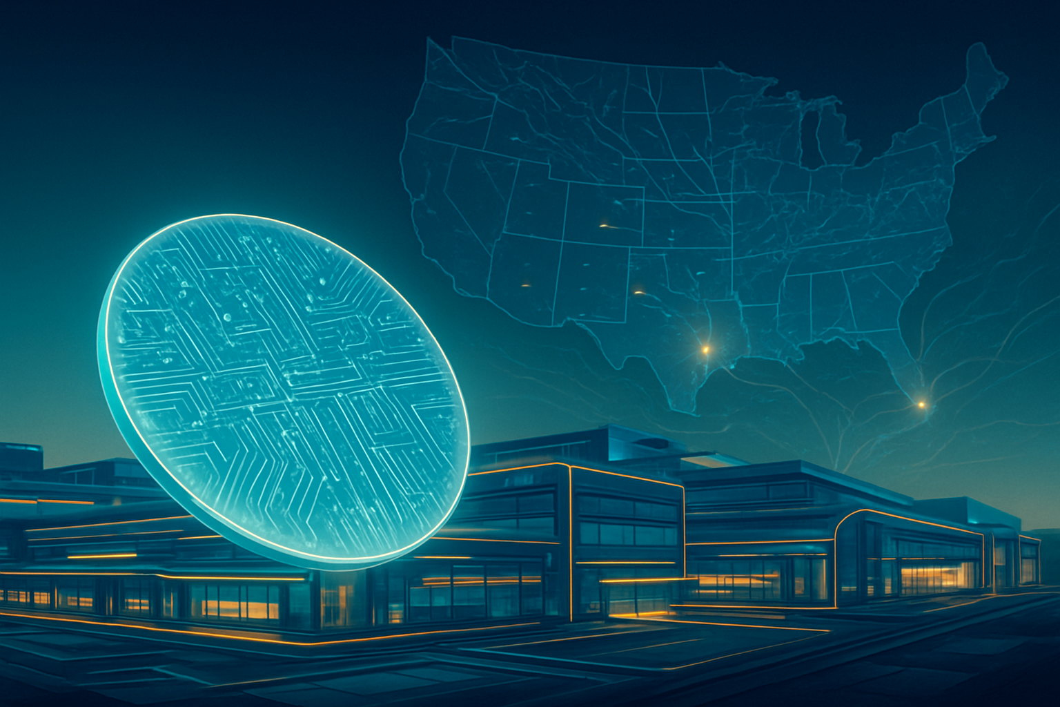
In a move that signals a seismic shift in the global technology landscape, the United States and Taiwan finalized a historic trade and investment agreement on January 15, 2026. The deal, spearheaded by the U.S. Department of Commerce, centers on a massive $250 billion direct investment pledge from Taiwanese industry titans to build advanced semiconductor and artificial intelligence production capacity on American soil. Combined with an additional $250 billion in credit guarantees from the Taiwanese government to support supply-chain migration, the $500 billion package represents the most significant effort in history to reshore the foundations of the digital age.
The agreement aims to fundamentally alter the geographical concentration of high-end computing. Its central strategic pillar is an ambitious goal to relocate 40% of Taiwan’s entire chip supply chain to the United States within the next few years. By creating a domestic "Silicon Shield," the U.S. hopes to secure its leadership in the AI revolution while mitigating the risks of regional instability in the Pacific. For Taiwan, the pact serves as a "force multiplier," ensuring that its "Sacred Mountain" of tech companies remains indispensable to the global economy through a permanent and integrated presence in the American industrial heartland.
The "Carrot and Stick" Framework: Section 232 and the Quota System
The technical core of the agreement revolves around a sophisticated utilization of Section 232 of the Trade Expansion Act, transforming traditional protectionist tariffs into powerful incentives for industrial relocation. To facilitate the massive capital flight required, the U.S. has introduced a "quota-based exemption" model. Under this framework, Taiwanese firms that commit to building new U.S.-based capacity are granted the right to import up to 2.5 times their planned U.S. production volume from their home facilities in Taiwan entirely duty-free during the construction phase. Once these facilities become operational, the companies maintain a 1.5-times duty-free import quota based on their actual U.S. output.
This mechanism is designed to prevent supply chain disruptions while the new American "Gigafabs" are being built. Furthermore, the agreement caps general reciprocal tariffs on a wide range of goods—including auto parts and timber—at 15%, down from previous rates that reached as high as 32% for certain sectors. For the AI research community, the inclusion of 0% tariffs on generic pharmaceuticals and specialized aircraft components is seen as a secondary but vital win for the broader high-tech ecosystem. Initial reactions from industry experts have been largely positive, with many praising the deal's pragmatic approach to bridging the cost gap between manufacturing in East Asia versus the United States.
Corporate Titans Lead the Charge: TSMC, Foxconn, and the 2nm Race
The success of the deal rests on the shoulders of Taiwan’s largest corporations. Taiwan Semiconductor Manufacturing Co., Ltd. (NYSE: TSM) has already confirmed that its 2026 capital expenditure will surge to a record $52 billion to $56 billion. As a direct result of the pact, TSM has acquired hundreds of additional acres in Arizona to create a "Gigafab" cluster. This expansion is not merely about volume; it includes the rapid deployment of 2nm production lines and advanced "CoWoS" packaging facilities, which are essential for the next generation of AI accelerators used by firms like NVIDIA Corp. (NASDAQ: NVDA).
Hon Hai Precision Industry Co., Ltd., better known as Foxconn (OTC: HNHPF), is also pivoting its U.S. strategy toward high-end AI infrastructure. Under the new trade framework, Foxconn is expanding its footprint to assemble the highly complex NVL 72 AI servers for NVIDIA and has entered a strategic partnership with OpenAI to co-design AI hardware components within the U.S. Meanwhile, MediaTek Inc. (TPE: 2454) is shifting its smartphone System-on-Chip (SoC) roadmap to utilize U.S.-based 2nm nodes, a strategic move to avoid potential 100% tariffs on foreign-made chips that could be applied to companies not participating in the reshoring initiative. This positioning grants these firms a massive competitive advantage, securing their access to the American market while stabilizing their supply lines against geopolitical volatility.
A New Era of Economic Security and Geopolitical Friction
This agreement is more than a trade deal; it is a declaration of economic sovereignty. By aiming to bring 40% of the supply chain to the U.S., the Department of Commerce is attempting to reverse a thirty-year decline in American wafer fabrication, which fell from a 37% global share in 1990 to less than 10% in 2024. The deal seeks to replicate Taiwan’s successful "Science Park" model in states like Arizona, Ohio, and Texas, creating self-sustaining industrial clusters where R&D and manufacturing exist side-by-side. This move is seen as the ultimate insurance policy for the AI era, ensuring that the hardware required for LLMs and autonomous systems is produced within a secure domestic perimeter.
However, the pact has not been without its detractors. Beijing has officially denounced the agreement as "economic plunder," accusing the U.S. of hollowing out Taiwan’s industrial base for its own gain. Within Taiwan, a heated debate persists regarding the "brain drain" of top engineering talent to the U.S. and the potential loss of the island's "Silicon Shield"—the theory that its dominance in chipmaking protects it from invasion. In response, Taiwanese Vice Premier Cheng Li-chiun has argued that the deal represents a "multiplication" of Taiwan's strength, moving from a single island fortress to a global distributed network that is even harder to disrupt.
The Road Ahead: 2026 and Beyond
Looking toward the near-term, the focus will shift from diplomatic signatures to industrial execution. Over the next 18 to 24 months, the tech industry will watch for the first "breaking of ground" on the new Gigafab sites. The primary challenge remains the development of a skilled workforce; the agreement includes provisions for "educational exchange corridors," but the sheer scale of the 40% reshoring goal will require tens of thousands of specialized engineers that the U.S. does not currently have in reserve.
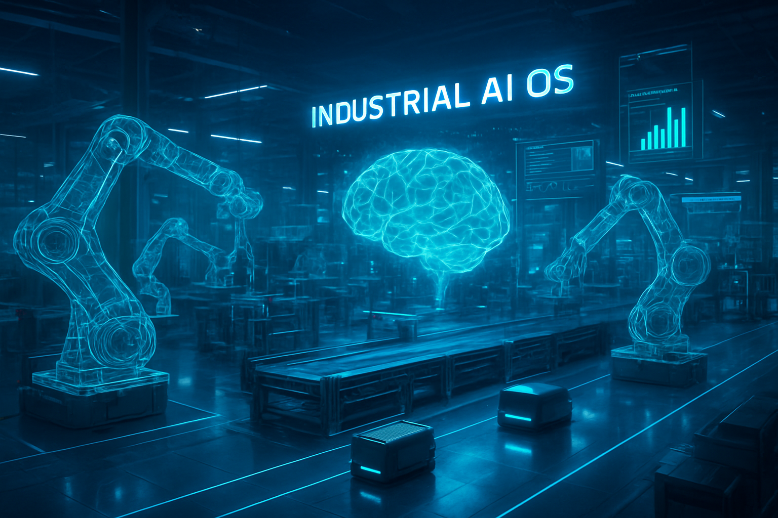
Experts predict that if the "2.5x/1.5x" quota system proves successful, it could serve as a blueprint for similar trade agreements with other key allies, such as Japan and South Korea. We may also see the emergence of "sovereign AI clouds"—compute clusters owned and operated within the U.S. using exclusively domestic-made chips—which would have profound implications for government and military AI applications. The long-term vision is a world where the hardware for artificial intelligence is no longer a bottleneck or a geopolitical flashpoint, but a commodity produced with American energy and labor.
Final Reflections on a Landmark Moment
The US-Taiwan Agreement of January 2026 marks a definitive turning point in the history of the information age. By successfully incentivizing a $250 billion private sector investment and securing a $500 billion total support package, the U.S. has effectively hit the "reset" button on global manufacturing. This is not merely an act of protectionism, but a massive strategic bet on the future of AI and the necessity of a resilient, domestic supply chain for the technologies that will define the rest of the century.
As we move forward, the key metrics of success will be the speed of fab construction and the ability of the U.S. to integrate these Taiwanese giants into its domestic economy without stifling innovation. For now, the message to the world is clear: the era of hyper-globalized, high-risk supply chains is ending, and the era of the "domesticated" AI stack has begun. Investors and industry watchers should keep a close eye on the quarterly Capex reports of TSMC and Foxconn throughout 2026, as these will be the first true indicators of how quickly this historic transition is taking hold.
This content is intended for informational purposes only and represents analysis of current AI developments.
TokenRing AI delivers enterprise-grade solutions for multi-agent AI workflow orchestration, AI-powered development tools, and seamless remote collaboration platforms.
For more information, visit https://www.tokenring.ai/.