Tag: Manufacturing

  • The Silicon Renaissance: How AI-Driven ‘Green Fabs’ are Solving the Semiconductor Industry’s Climate Crisis

    The Silicon Renaissance: How AI-Driven ‘Green Fabs’ are Solving the Semiconductor Industry’s Climate Crisis

    The global semiconductor industry, long criticized for its massive environmental footprint, has reached a pivotal turning point as of early 2026. Facing a "Green Paradox"—where the exponential demand for power-hungry AI chips threatens to derail global climate goals—industry titans are pivoting toward a new era of sustainable "Green Fabs." By integrating advanced artificial intelligence and circular manufacturing principles, these massive fabrication plants are transforming from resource-draining monoliths into highly efficient, self-optimizing ecosystems that dramatically reduce water consumption, electricity use, and carbon emissions.

    This shift is not merely a corporate social responsibility initiative but a fundamental necessity for the industry's survival. As manufacturing moves toward 2nm and below, the energy and water intensity of chip production has skyrocketed. However, the same AI technologies that drive this demand are now being deployed to solve the problem. Through the use of autonomous digital twins and AI-managed resource streams, companies like Intel (NASDAQ: INTC) and TSMC (NYSE: TSM) are proving that the future of high-performance computing can, and must, be green.

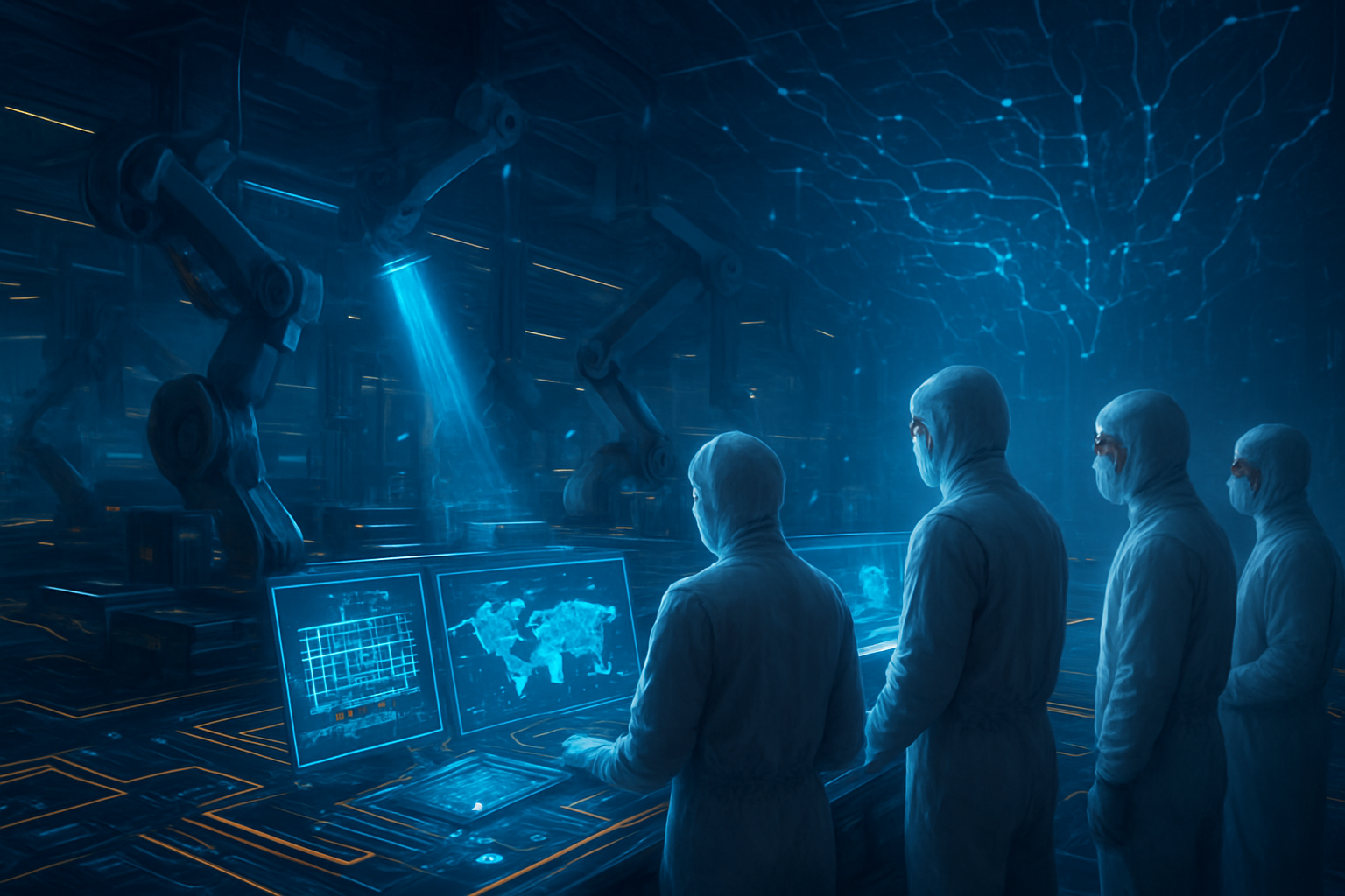
    The Rise of the Autonomous Digital Twin

    The technical backbone of the Green Fab movement is the "Autonomous Digital Twin." In January 2026, Samsung (KRX: 005930) and NVIDIA (NASDAQ: NVDA) announced the full-scale deployment of a digital twin model across Samsung’s Hwaseong and Pyeongtaek campuses. This system uses over 50,000 GPUs to create a high-fidelity virtual replica of the entire fabrication process. Unlike previous simulation models, these AI-driven twins analyze operational data from millions of sensors in real-time, simulating airflow, chemical distribution, and power loads with unprecedented accuracy. Samsung reports that this "AI Brain" has improved energy efficiency by nearly 20 times compared to legacy manual systems, allowing for real-time adjustments that prevent waste before it occurs.

    Furthering this technical leap, Siemens (OTC: SIEGY) and NVIDIA recently unveiled an "Industrial AI Operating System" that provides a repeatable blueprint for next-generation factories. This system utilizes a "Digital Twin Composer" to allow fabs to test energy-saving changes virtually before implementing them on the physical shop floor. Meanwhile, Synopsys (NASDAQ: SNPS) has introduced AI-driven "Electronics Digital Twins" that enable "Shift Left" verification. This technology allows engineers to predict the carbon footprint and energy performance of a chip's manufacturing process during the design phase, ensuring sustainability is "baked in" before a single wafer is etched.

    These advancements differ from previous approaches by moving away from reactive monitoring toward proactive, predictive management. In the past, water and energy use were managed through static benchmarks; today, AI agents monitor over 20 segregated chemical waste streams and adjust filtration pressures and chemical dosing dynamically. This level of precision is essential for managing the extreme complexity of modern sub-2nm nodes, where even microscopic contamination can ruin entire batches and lead to massive resource waste.

    Strategic Advantages in the Green Silicon Race

    The transition to Green Fabs is creating a new competitive landscape where environmental efficiency is a primary market differentiator. Companies like Applied Materials (NASDAQ: AMAT) and ASML (NASDAQ: ASML) stand to benefit significantly as they provide the specialized tools required for this transition. Applied Materials has launched its "3×30" initiative, aiming for a 30% reduction in energy, chemicals, and floorspace per wafer by 2030. Their SuCCESS2030 program also mandates that 80% of supplier packaging be made from recycled content, pushing circularity throughout the entire supply chain.

    For major chipmakers, "Green Silicon" has become a strategic advantage when bidding for contracts from tech giants like Apple (NASDAQ: AAPL) and Alphabet (NASDAQ: GOOGL), both of which have aggressive net-zero goals for their entire value chains. TSMC has responded by accelerating its RE100 goal (100% renewable energy) to 2040, a full decade earlier than its original target. By securing massive amounts of renewable energy and implementing 90% water recycling rates at its new Arizona facilities, TSMC is positioning itself as the preferred partner for environmentally conscious tech leaders.

    This shift also disrupts the traditional "growth at any cost" model. Smaller startups and legacy fabs that cannot afford the high capital expenditure required for AI-driven sustainability may find themselves at a disadvantage, as regulatory pressures—particularly in the EU and the United States—begin to favor "Net Zero" manufacturing. The ability to reclaim 95% of parts, a feat recently achieved by ASML’s "House of Re-use" program, is becoming the gold standard for operational efficiency and cost reduction in a world of fluctuating raw material prices.

    Geopolitics, Water, and the Broader AI Landscape

    The significance of the Green Fab movement extends far beyond the balance sheets of semiconductor companies. It fits into a broader global trend where the physical limits of our planet are beginning to dictate the pace of technological advancement. Fabs are now evolving into "Zero-Liquid Discharge" (ZLD) ecosystems, which is critical in water-stressed regions like Arizona and Taiwan. Intel, for instance, has achieved "Net Positive Water" status at its Arizona Fab 52, restoring approximately 107% of the water it uses back to local watersheds.

    However, this transition is not without its concerns. The sheer amount of compute power required to run these AI-driven "Green Brains" creates its own energy demand. Critics point to the irony of using thousands of GPUs to save energy, though proponents argue that the 20x efficiency gains far outweigh the power consumed by the AI itself. This development also highlights the geopolitical importance of resource security; as fabs become more circular, they become less dependent on global supply chains for rare gases like neon and specialized chemicals, making them more resilient to international conflicts and trade disputes.

    Comparatively, this milestone is as significant as the shift from 200mm to 300mm wafers. It represents a fundamental change in how the industry views its relationship with the environment. In the same way that Moore’s Law drove the miniaturization of transistors, the new "Green Law" is driving the optimization of the manufacturing environment itself, ensuring that the digital revolution does not come at the expense of a habitable planet.

    The Road to 2040: What Lies Ahead

    In the near term, we can expect to see the widespread adoption of "Industrial AI Agents" that operate with increasing autonomy. These agents will eventually move beyond simple optimization to "lights-out" manufacturing, where AI manages the entire fab environment with minimal human intervention. This will further reduce energy use by eliminating the need for human-centric lighting and climate control in many parts of the plant.

    Longer-term developments include the integration of new, more efficient materials like Gallium Nitride (GaN) and Silicon Carbide (SiC) into the fab infrastructure itself. Experts predict that by 2030, the "Zero-Liquid Discharge" model will become the industry standard for all new construction. The challenge remains in retrofitting older, legacy fabs with these advanced AI systems, a process that is both costly and technically difficult. However, as AI-driven digital twins become more accessible, even older plants may see a "green second life" through software-based optimizations.

    Predicting the next five years, industry analysts suggest that the focus will shift from Scope 1 and 2 emissions (direct operations and purchased energy) to the much more difficult Scope 3 emissions (the entire value chain). This will require an unprecedented level of data sharing between suppliers, manufacturers, and end-users, all facilitated by secure, AI-powered transparency platforms.

    A Sustainable Blueprint for the Future

    The move toward sustainable Green Fabs represents a landmark achievement in the history of industrial manufacturing. By leveraging AI to manage the staggering complexity of chip production, the semiconductor industry is proving that it is possible to decouple technological growth from environmental degradation. The key takeaways are clear: AI is no longer just the product being made; it is the essential tool that makes the production process viable in a climate-constrained world.

    As we look toward the coming months, watch for more partnerships between industrial giants and AI leaders, as well as new regulatory frameworks that may mandate "Green Silicon" certifications. The success of these initiatives will determine whether the AI revolution can truly be a force for global progress or if it will be hindered by its own resource requirements. For now, the "Green Fab" stands as a beacon of hope—a high-tech solution to a high-tech problem, ensuring that the chips of tomorrow are built on a foundation of sustainability.


    This content is intended for informational purposes only and represents analysis of current AI developments.

    TokenRing AI delivers enterprise-grade solutions for multi-agent AI workflow orchestration, AI-powered development tools, and seamless remote collaboration platforms.
    For more information, visit https://www.tokenring.ai/.

  • Powering the Future: Onsemi and GlobalFoundries Forge “Made in America” GaN Alliance for AI and EVs

    Powering the Future: Onsemi and GlobalFoundries Forge “Made in America” GaN Alliance for AI and EVs

    In a move set to redefine the power semiconductor landscape, onsemi (NASDAQ: ON) and GlobalFoundries (NASDAQ: GFS) have announced a strategic collaboration to develop and manufacture 650V Gallium Nitride (GaN) power devices. This partnership, finalized in late December 2025, marks a critical pivot in the industry as it transitions from traditional 150mm wafers to high-volume 200mm GaN-on-silicon manufacturing. By combining onsemi’s leadership in power systems with GlobalFoundries’ large-scale U.S. fabrication capabilities, the alliance aims to address the skyrocketing energy demands of AI data centers and the efficiency requirements of next-generation electric vehicles (EVs).

    The immediate significance of this announcement lies in its creation of a robust, domestic "Made in America" supply chain for wide-bandgap semiconductors. As the global tech industry faces increasing geopolitical pressures and supply chain volatility, the onsemi-GlobalFoundries partnership offers a secure, high-capacity source for the critical components that power the modern digital and green economy. With customer sampling scheduled to begin in the first half of 2026, the collaboration is poised to dismantle the "power wall" that has long constrained the performance of high-density server racks and the range of electric transport.

    Scaling the Power Wall: The Shift to 200mm GaN-on-Silicon

    The technical cornerstone of this collaboration is the development of 650V enhancement-mode (eMode) lateral GaN-on-silicon power devices. Unlike traditional silicon-based MOSFETs, GaN offers significantly higher electron mobility and breakdown strength, allowing for faster switching speeds and reduced thermal losses. The move to 200mm (8-inch) wafers is a game-changer; it provides a substantial increase in die count per wafer compared to the previous 150mm industry standard, effectively lowering the unit cost and enabling the economies of scale necessary for mass-market adoption.

    Technically, the 650V rating is the "sweet spot" for high-efficiency power conversion. Onsemi is integrating its proprietary silicon drivers, advanced controllers, and thermally enhanced packaging with GlobalFoundries’ specialized GaN process. This "system-in-package" approach allows for bidirectional power flow and integrated protection, which is vital for the high-frequency switching environments of AI power supplies. By operating at higher frequencies, these GaN devices allow for the use of smaller passive components, such as inductors and capacitors, leading to a dramatic increase in power density—essentially packing more power into a smaller physical footprint.

    Initial reactions from the industry have been overwhelmingly positive. Power electronics experts note that the transition to 200mm manufacturing is the "tipping point" for GaN technology to move from niche applications to mainstream infrastructure. While previous GaN efforts were often hampered by yield issues and high costs, the combined expertise of these two giants—utilizing GlobalFoundries’ mature CMOS-compatible fabrication processes—suggests a level of reliability and volume that has previously eluded domestic GaN production.

    Strategic Dominance: Reshaping the Semiconductor Supply Chain

    The collaboration places onsemi (NASDAQ: ON) and GlobalFoundries (NASDAQ: GFS) in a formidable market position. For onsemi, the partnership accelerates its roadmap to a complete GaN portfolio, covering low, medium, and high voltage applications. For GlobalFoundries, it solidifies its role as the premier U.S. foundry for specialized power technologies. This is particularly timely following Taiwan Semiconductor Manufacturing Company’s (NYSE: TSM) announcement that it would exit the GaN foundry service market by 2027. By licensing TSMC’s 650V GaN technology in late 2025, GlobalFoundries has effectively stepped in to fill a massive vacuum in the global foundry landscape.

    Major tech giants building out AI infrastructure, such as Microsoft (NASDAQ: MSFT) and Google (NASDAQ: GOOGL), stand to benefit significantly. As AI server racks now demand upwards of 100kW per rack, the efficiency gains provided by 650V GaN are no longer optional—they are a prerequisite for managing operational costs and cooling requirements. Furthermore, domestic automotive manufacturers like Ford (NYSE: F) and General Motors (NYSE: GM) gain a strategic advantage by securing a U.S.-based source for onboard chargers (OBCs) and DC-DC converters, helping them meet local-content requirements and insulate their production lines from overseas disruptions.

    The competitive implications are stark. This alliance creates a "moat" around the U.S. power semiconductor industry, leveraging CHIPS Act funding—including the $1.5 billion previously awarded to GlobalFoundries—to build a manufacturing powerhouse. Existing players who rely on Asian foundries for GaN production may find themselves at a disadvantage as "Made in America" mandates become more prevalent in government and defense-linked aerospace projects, where thermal efficiency and supply chain security are paramount.

    The AI and Electrification Nexus: Broadening the Horizon

    This development fits into a broader global trend where the energy transition and the AI revolution are converging. The massive energy footprint of generative AI has forced a reckoning in data center design. GaN technology is a key pillar of this transformation, enabling the high-efficiency power delivery units (PDUs) required to keep pace with the power-hungry GPUs and TPUs driving the AI boom. By reducing energy waste at the conversion stage, these 650V devices directly contribute to the decarbonization goals of the world’s largest technology firms.

    The "Made in America" aspect cannot be overstated. By centering production in Malta, New York, and Burlington, Vermont, the partnership revitalizes U.S. manufacturing in a sector that was once dominated by offshore facilities. This shift mirrors the earlier transition from silicon to Silicon Carbide (SiC) in the EV industry, but with GaN offering even greater potential for high-frequency applications and consumer electronics. The move signals a broader strategic intent to maintain technological sovereignty in the foundational components of the 21st-century economy.

    However, the transition is not without its hurdles. While the performance benefits of GaN are clear, the industry must still navigate the complexities of integrating these new materials into existing system architectures. There are also concerns regarding the long-term reliability of GaN-on-silicon under the extreme thermal cycling found in automotive environments. Nevertheless, the collaboration between onsemi and GlobalFoundries represents a major milestone, comparable to the initial commercialization of the IGBT in the 1980s, which revolutionized industrial motor drives.

    From Sampling to Scale: What Lies Ahead for GaN

    In the near term, the focus will be on the successful rollout of customer samples in the first half of 2026. This period will be critical for validating the performance and reliability of the 200mm GaN-on-silicon process in real-world conditions. Beyond AI data centers and EVs, the horizon for these 650V devices includes applications in solar microinverters and energy storage systems (ESS), where high-efficiency DC-to-AC conversion is essential for maximizing the output of renewable energy sources.

    Experts predict that as manufacturing yields stabilize on the 200mm platform, we will see a rapid decline in the cost-per-watt of GaN devices, potentially reaching parity with high-end silicon MOSFETs by late 2027. This would trigger a second wave of adoption in consumer electronics, such as ultra-fast chargers for laptops and smartphones. The next technical frontier will likely involve the development of 800V and 1200V GaN devices to support the 800V battery architectures becoming common in high-performance electric vehicles.

    The primary challenge remaining is the talent gap in wide-bandgap semiconductor engineering. As manufacturing returns to U.S. soil, the demand for specialized engineers who understand the nuances of GaN design and fabrication is expected to surge. Both onsemi and GlobalFoundries are likely to increase their investments in university partnerships and domestic training programs to ensure the long-term viability of this new manufacturing ecosystem.

    A New Era of Domestic Power Innovation

    The collaboration between onsemi and GlobalFoundries is more than just a business deal; it is a strategic realignment of the power semiconductor industry. By focusing on 650V GaN-on-silicon at the 200mm scale, the two companies are positioning themselves at the heart of the AI and EV revolutions. The key takeaways are clear: domestic manufacturing is back, GaN is ready for the mainstream, and the "power wall" is finally being breached.

    In the context of semiconductor history, this partnership may be viewed as the moment when the United States reclaimed its lead in power electronics manufacturing. The long-term impact will be felt in more efficient data centers, faster-charging EVs, and a more resilient global supply chain. In the coming weeks and months, the industry will be watching closely for the first performance data from the 200mm pilot lines and for further announcements regarding the expansion of this GaN platform into even higher voltage ranges.


    This content is intended for informational purposes only and represents analysis of current AI developments.

    TokenRing AI delivers enterprise-grade solutions for multi-agent AI workflow orchestration, AI-powered development tools, and seamless remote collaboration platforms.
    For more information, visit https://www.tokenring.ai/.

  • The Human Wall: Global Talent Shortage Threatens the $1 Trillion Semiconductor Milestone

    The Human Wall: Global Talent Shortage Threatens the $1 Trillion Semiconductor Milestone

    As of January 2026, the global semiconductor industry finds itself at a paradoxical crossroads. While the demand for high-performance silicon—fueled by an insatiable appetite for generative AI and autonomous systems—has the industry on a clear trajectory to reach $1 trillion in annual revenue by 2030, a critical resource is running dry: human expertise. The sector is currently facing a projected deficit of more than 1 million skilled workers by the end of the decade, a "human wall" that threatens to stall the most ambitious manufacturing expansion in history.

    This talent crisis is no longer a peripheral concern for HR departments; it has become a primary bottleneck for national security and economic sovereignty. From the sun-scorched "Silicon Desert" of Arizona to the stalled "Silicon Junction" in Europe, the inability to find, train, and retain specialized engineers is forcing multi-billion dollar projects to be delayed, downscaled, or abandoned entirely. As the industry races toward the 2nm node and beyond, the gap between technical ambition and labor availability has reached a breaking point.

    The Technical Deficit: Precision Engineering Meets a Shrinking Workforce

    The technical specifications of modern semiconductor manufacturing have evolved faster than the educational pipelines supporting them. Today’s leading-edge facilities, such as Intel Corporation (NASDAQ: INTC) Fab 52 in Arizona, are now utilizing High-NA EUV (Extreme Ultraviolet) lithography to produce 18A (1.8nm) process chips. These machines, costing upwards of $350 million each, require a level of operational expertise that did not exist five years ago. According to data from SEMI, global front-end capacity is growing at a 7% CAGR, but the demand for advanced node specialists (7nm and below) is surging at double that rate.

    The complexity of these new nodes means that the "learning curve" for a new engineer has lengthened significantly. A process engineer at Taiwan Semiconductor Manufacturing Co. (NYSE: TSM) now requires years of highly specialized training to manage the chemical vapor deposition and plasma etching processes required for gate-all-around (GAA) transistor architectures. This differs fundamentally from previous decades, where mature nodes were more forgiving and the workforce was more abundant. Initial reactions from the research community suggest that without a radical shift in how we automate the "art" of chipmaking, the physical limits of human scaling will be reached before the physical limits of silicon.

    Industry experts at Deloitte and McKinsey have highlighted that the crisis is not just about PhD-level researchers. There is a desperate shortage of "cleanroom-ready" technicians and maintenance staff. In the United States alone, the industry needs to hire roughly 100,000 new workers annually to meet 2030 targets, yet the current graduation rate for relevant engineering degrees is less than half of that. This mismatch has turned every new fab announcement into a high-stakes gamble on local labor markets.

    A Zero-Sum Game: Corporate Poaching and the "Sexiness" Gap

    The talent war has created a cutthroat environment where established giants and cash-flush software titans are cannibalizing the same limited pool of experts. In Arizona, a localized arms race has broken out between TSMC and Intel. While TSMC’s first Phoenix fab has finally achieved mass production of 4nm chips with yields exceeding 92%, it has done so by rotating over 500 Taiwanese engineers through the site to compensate for local shortages. Meanwhile, Intel has aggressively poached senior staff from its rivals to bolster its nascent Foundry services, turning the Phoenix metro area into a zero-sum game for talent.

    The competitive landscape is further complicated by the entry of "hyperscalers" into the custom silicon space. Alphabet Inc. (NASDAQ: GOOGL), Meta Platforms Inc. (NASDAQ: META), and Amazon.com Inc. (NASDAQ: AMZN) are no longer just customers; they are designers. By developing their own AI-specific chips, such as Google’s TPU, these software giants are successfully luring "backend" designers away from traditional firms like Broadcom Inc. (NASDAQ: AVGO) and Marvell Technology Inc. (NASDAQ: MRVL). These software firms offer compensation packages—often including lucrative stock options—and a "sexiness" work culture that traditional manufacturing firms struggle to match.

    Nvidia Corporation (NASDAQ: NVDA) currently stands as the ultimate victor in this recruitment battle. With its market cap and R&D budget dwarfing many of its peers, Nvidia has become the "employer of choice," reportedly offering signing bonuses for top-tier AI and chip architecture talent that exceed $100 million in total compensation over several years. This leaves traditional manufacturers like STMicroelectronics NV (NYSE: STM) and GlobalFoundries Inc. (NASDAQ: GFS) in a difficult position, struggling to staff their mature-node facilities which remain essential for the automotive and industrial sectors.

    The "Silver Tsunami" and the Geopolitics of Labor

    Beyond the corporate competition, the semiconductor industry is facing a demographic crisis often referred to as the "Silver Tsunami." Data from Lightcast in early 2026 indicates that nearly 80% of the workers who have exited the manufacturing workforce since 2021 were over the age of 55. This isn't just a loss of headcount; it is a catastrophic drain of institutional knowledge. The "founding generation" of engineers who understood the nuances of yield management and equipment maintenance is retiring, and McKinsey reports that only 57% of this expertise has been successfully transferred to younger hires.

    This demographic shift has severe implications for regional ambitions. The European Union’s goal to reach 20% of global market share by 2030 is currently in jeopardy. In mid-2025, Intel officially withdrew from its €30 billion mega-fab project in Magdeburg, Germany, citing a lack of committed customers and, more critically, a severe shortage of specialized labor. SEMI Europe estimates the region still needs 400,000 additional professionals by 2030, a target that seems increasingly unreachable as younger generations in Europe gravitate toward software and service sectors rather than hardware manufacturing.

    This crisis also intersects with national security. The U.S. CHIPS Act was designed to reshore manufacturing, but without a corresponding "Talent Act," the infrastructure may sit idle. The reliance on H-1B visas and international talent remains a flashpoint; while the industry pleads for more flexible immigration policies to bring in experts from Taiwan and South Korea, political headwinds often favor domestic-only hiring, further constricting the talent pipeline.

    The Path Forward: AI-Driven Design and Educational Reform

    To address the 1 million worker gap, the industry is looking toward two primary solutions: automation and radical educational reform. Near-term developments are focused on "AI for Silicon," where generative AI tools are used to automate the physical layout and verification of chips. Companies like Synopsys Inc. (NASDAQ: SNPS) and Cadence Design Systems Inc. (NASDAQ: CDNS) are pioneering AI-driven EDA (Electronic Design Automation) tools that can perform tasks in weeks that previously took teams of engineers months. This "talent multiplier" effect may be the only way to meet the 2030 goals without a 1:1 increase in headcount.

    In the long term, we expect to see a massive shift in how semiconductor education is delivered. "Micro-credentials" and specialized vocational programs are being developed in partnership with community colleges in Arizona and Ohio to create a "technician class" that doesn't require a four-year degree. Furthermore, experts predict that the industry will increasingly turn to "remote fab management," using digital twins and augmented reality to allow senior engineers in Taiwan or Oregon to troubleshoot equipment in Germany or Japan, effectively "stretching" the existing talent pool across time zones.

    However, challenges remain. The "yield risk" associated with a less experienced workforce is real, and the cost of training is soaring. If the industry cannot solve the "sexiness" problem and convince Gen Z that building the hardware of the future is as prestigious as writing the software that runs on it, the $1 trillion goal may remain a pipe dream.

    Summary: A Crisis of Success

    The semiconductor talent war is the defining challenge of the mid-2020s. The industry has succeeded in making itself the most important sector in the global economy, but it has failed to build a sustainable human infrastructure to support its own growth. The key takeaways are clear: the 1 million worker gap is a systemic threat, the "Silver Tsunami" is eroding the industry's knowledge base, and the competition from software giants is making recruitment harder than ever.

    As we move through 2026, the industry's significance in AI history will be determined not just by how many transistors can fit on a chip, but by how many engineers can be trained to put them there. Watch for significant policy shifts regarding "talent visas" and a surge in M&A activity as larger firms acquire smaller ones simply for their "acqui-hire" value. The talent war is no longer a skirmish; it is a full-scale battle for the future of technology.


    This content is intended for informational purposes only and represents analysis of current AI developments.

    TokenRing AI delivers enterprise-grade solutions for multi-agent AI workflow orchestration, AI-powered development tools, and seamless remote collaboration platforms.
    For more information, visit https://www.tokenring.ai/.

  • Silicon Sovereignty: Texas Instruments’ SM1 Fab Marks a New Era for American Chipmaking

    Silicon Sovereignty: Texas Instruments’ SM1 Fab Marks a New Era for American Chipmaking

    The landscape of American industrial power shifted decisively this week as Texas Instruments (NASDAQ: TXN) officially commenced high-volume production at its landmark SM1 fabrication plant in Sherman, Texas. The opening of the $30 billion facility represents the first major "foundational" chip plant to go online under the auspices of the CHIPS and Science Act, signaling a robust return of domestic semiconductor manufacturing. While much of the global conversation has focused on the race for sub-2nm logic, the SM1 fab addresses a critical vulnerability in the global supply chain: the analog and embedded chips that serve as the nervous system for everything from electric vehicles to AI data center power management.

    This milestone is more than just a corporate expansion; it is a centerpiece of a broader national strategy to insulate the U.S. economy from geopolitical shocks. As of January 2026, the "Silicon Resurgence" is no longer a legislative ambition but a physical reality. The SM1 fab is the first of four planned facilities on the Sherman campus, part of a staggering $60 billion investment by Texas Instruments to ensure that the foundational silicon required for the next decade of technological growth is "Made in America."

    The Architecture of Resilience: Inside the SM1 Fab

    The SM1 facility is a technological marvel designed for efficiency and scale, utilizing 300mm wafer technology to drive down costs and increase output. Unlike the leading-edge logic fabs being built by competitors, TI’s Sherman site focuses on specialty process nodes ranging from 28nm to 130nm. While these may seem "mature" compared to the latest 1.8nm breakthroughs, they are technically optimized for analog and embedded processing. These chips are essential for high-voltage power delivery, signal conditioning, and real-time control—functions that cannot be performed by high-end GPUs alone. The fab's integration of advanced automation and sustainable manufacturing practices allows it to achieve yields that rival the most efficient plants in Southeast Asia.

    The technical significance of SM1 lies in its role as a "foundational" supplier. During the semiconductor shortages of 2021-2022, it was often these $1 analog chips, rather than $1,000 CPUs, that halted automotive production lines. By securing domestic production of these components, the U.S. is effectively building a floor under its industrial stability. This differs from previous decades of "fab-lite" strategies where U.S. firms outsourced manufacturing to focus solely on design. Today, TI is vertically integrating its supply chain, a move that industry experts at the Semiconductor Industry Association (SIA) suggest will provide a significant competitive advantage in terms of lead times and quality control for the automotive and industrial sectors.

    A New Competitive Landscape for AI and Big Tech

    The resurgence of domestic manufacturing is creating a ripple effect across the technology sector. While Texas Instruments (NASDAQ: TXN) secures the foundational layer, Intel (NASDAQ: INTC) has simultaneously entered high-volume manufacturing with its Intel 18A (1.8nm) process at Fab 52 in Arizona. This dual-track progress—foundational chips in Texas and leading-edge logic in Arizona—benefits a wide array of tech giants. Nvidia (NASDAQ: NVDA) and Apple (NASDAQ: AAPL) are already reaping the benefits of diversified geographic footprints, as TSMC (NYSE: TSM) has stabilized its Phoenix operations, producing 4nm and 5nm chips with yields comparable to its Taiwan facilities.

    For AI startups and enterprise hardware firms, the proximity of these fabs reduces the logistical risks associated with the "Taiwan Strait bottleneck." The strategic advantage is clear: companies can now design, manufacture, and package high-performance AI silicon entirely within the North American corridor. Samsung (KRX: 005930) is also playing a pivotal role, with its Taylor, Texas facility currently installing equipment for 2nm Gate-All-Around (GAA) technology. This creates a highly competitive environment where U.S.-based customers can choose between three of the world’s leading foundries—Intel, TSMC, and Samsung—all operating on U.S. soil.

    The "Silicon Shield" and the Global AI Race

    The opening of SM1 and the broader domestic manufacturing boom represent a fundamental shift in the global AI landscape. For years, the concentration of chip manufacturing in East Asia was viewed as a single point of failure for the global digital economy. The CHIPS Act has acted as a catalyst, providing TI with $1.6 billion in direct funding and an estimated $6 billion to $8 billion in investment tax credits. This government-backed de-risking has turned the U.S. into a "Silicon Shield," protecting the infrastructure required for the AI revolution from external disruptions.

    However, this transition is not without its concerns. The rapid expansion of these "megafabs" has strained local power grids and water supplies, particularly in the arid regions of Texas and Arizona. Furthermore, the industry faces a looming talent gap; experts estimate the U.S. will need an additional 67,000 semiconductor workers by 2030. Comparisons are frequently drawn to the 1980s, when the U.S. nearly lost its chipmaking edge to Japan. The current resurgence is viewed as a successful "second act" for American manufacturing, but one that requires sustained long-term investment rather than a one-time legislative infusion.

    The Road to 2030: What Lies Ahead

    Looking forward, the Sherman campus is just beginning its journey. Construction on SM2 is already well underway, with plans for SM3 and SM4 to follow as market demand for AI-driven power management grows. In the near term, we expect to see the first "all-American" AI servers—featuring Intel 18A processors, Micron (NASDAQ: MU) HBM3E memory, and TI power management chips—hitting the market by late 2026. This vertical domestic supply chain will be a game-changer for government and defense applications where security and provenance are paramount.

    The next major hurdle will be the integration of advanced packaging. While the U.S. has made strides in wafer fabrication, much of the "back-end" assembly and testing still occurs overseas. Experts predict that the next wave of CHIPS Act funding and private investment will focus heavily on domesticating these advanced packaging technologies, which are essential for stacking chips in the 3D configurations required for next-generation AI accelerators.

    A Milestone in the History of Computing

    The operational start of the SM1 fab is a watershed moment for the American semiconductor industry. It marks the transition from planning to execution, proving that the U.S. can still build world-class industrial infrastructure at scale. By 2030, the Department of Commerce expects the U.S. to produce 20% of the world’s leading-edge logic chips, up from 0% just four years ago. This resurgence ensures that the "intelligence" of the 21st century—the silicon that powers our AI, our vehicles, and our infrastructure—is built on a foundation of domestic resilience.

    As we move into the second half of the decade, the focus will shift from "can we build it?" to "can we sustain it?" The success of the Sherman campus and its counterparts in Arizona and Ohio will be measured not just by wafer starts, but by their ability to foster a self-sustaining ecosystem of innovation. For now, the lights are on in Sherman, and the first wafers are moving through the line, signaling that the heart of the digital world is beating stronger than ever in the American heartland.


    This content is intended for informational purposes only and represents analysis of current AI and semiconductor developments.

    TokenRing AI delivers enterprise-grade solutions for multi-agent AI workflow orchestration, AI-powered development tools, and seamless remote collaboration platforms.
    For more information, visit https://www.tokenring.ai/.

  • Silicon Sovereignty: Texas Instruments’ SM1 Fab Leads the Charge in America’s Semiconductor Renaissance

    Silicon Sovereignty: Texas Instruments’ SM1 Fab Leads the Charge in America’s Semiconductor Renaissance

    The landscape of American technology has reached a historic milestone as Texas Instruments (NASDAQ: TXN) officially enters its "Harvest Year," marked by the successful production launch of its landmark SM1 fab in Sherman, Texas. This facility, which began high-volume operations on December 17, 2025, represents the first major wave of domestic semiconductor capacity coming online under the strategic umbrella of the CHIPS and Science Act. As of January 2026, the SM1 fab is actively ramping up to produce tens of millions of analog and embedded processing chips daily, signaling a decisive shift in the global supply chain.

    The activation of SM1 is more than a corporate achievement; it is a centerpiece of the United States' broader effort to secure the foundational silicon required for the AI revolution. While high-profile logic chips often dominate the headlines, the analog and power management components produced at the Sherman site are the indispensable "nervous system" of modern technology. Backed by a final award of $1.6 billion in direct federal funding and up to $8 billion in investment tax credits, Texas Instruments is now positioned to provide the stable, domestic hardware foundation necessary for everything from AI-driven data centers to the next generation of autonomous electric vehicles.

    The SM1 facility is a marvel of modern industrial engineering, specifically optimized for the production of 300mm (12-inch) wafers. By utilizing 300mm technology rather than the older 200mm industry standard, Texas Instruments achieves a 2.3-fold increase in surface area per wafer, which translates to a staggering 40% reduction in chip-level fabrication costs. This efficiency is critical for the "mature" nodes the facility targets, ranging from 28nm to 130nm. While these are not the sub-5nm nodes used for high-end CPUs, they are the gold standard for high-precision analog and power management applications where reliability and voltage tolerance are paramount.

    Technically, the SM1 fab is designed to be the most automated and environmentally sustainable facility in the company’s history. It features advanced cleanroom robotics and real-time AI-driven yield management systems that minimize waste and maximize throughput. This differs significantly from previous generations of manufacturing, which relied on more fragmented, manual oversight. The integration of these technologies allows TI to maintain a "fab-lite" level of flexibility while reaping the benefits of total internal manufacturing control—a strategy the company expects will lead to over 95% internal wafer production by 2030.

    Initial reactions from the industry and the research community have been overwhelmingly positive. Analysts at major firms note that the sheer scale of the Sherman site—which has the footprint to eventually house four massive fabs—provides a level of supply chain predictability that has been missing since the 2021 shortages. Experts highlight that TI's focus on foundational silicon addresses a critical bottleneck: you cannot run a $40,000 AI GPU without the $2 power management integrated circuits (PMICs) that regulate its energy intake. By securing this "bottom-up" capacity, the U.S. is effectively de-risking the entire hardware stack.

    The implications for the broader tech industry are profound, particularly for companies reliant on stable hardware pipelines. Texas Instruments stands as the primary beneficiary, leveraging its domestic footprint to gain a competitive edge over international rivals like STMicroelectronics or Infineon. By producing chips in the U.S., TI offers its customers—ranging from industrial giants to automotive leaders—a hedge against geopolitical instability and shipping disruptions. This strategic positioning is already paying dividends, as TI recently debuted its TDA5 SoC family at CES 2026, targeting Level 3 vehicle autonomy with chips manufactured right in North Texas.

    Major AI players, including NVIDIA (NASDAQ: NVDA) and Advanced Micro Devices (NASDAQ: AMD), also stand to benefit indirectly. The energy demands of AI data centers have skyrocketed, requiring sophisticated power modules and Gallium Nitride (GaN) semiconductors to maintain efficiency. TI’s new capacity is specifically geared toward these high-voltage applications. As domestic capacity grows, these tech giants can source essential peripheral components from a local partner, reducing lead times and ensuring that the massive infrastructure build-out for generative AI continues without the "missing link" component shortages of years past.

    Furthermore, the domestic boom is forcing a strategic pivot among startups and mid-sized tech firms. With guaranteed access to U.S.-made silicon, developers in the robotics and IoT sectors can design products with a "Made in USA" assurance, which is increasingly becoming a requirement for government and defense contracts. This could potentially disrupt the market positioning of offshore foundries that have traditionally dominated the mature-node space. As Texas Instruments ramps up SM1 and prepares its sister facilities, the competitive landscape is shifting from a focus on "cheapest possible" to "most resilient and reliable."

    Looking at the wider significance, the SM1 launch is a tangible validation of the CHIPS and Science Act’s long-term vision. It marks a transition from legislative intent to industrial reality. In the broader AI landscape, this development signifies the "hardware hardening" phase of the AI era. While 2023 and 2024 were defined by software breakthroughs and LLM scaling, 2025 and 2026 are being defined by the physical infrastructure required to sustain those gains. The U.S. is effectively building a "silicon shield" that protects its technological lead from external supply shocks.

    However, this expansion is not without its concerns. The rapid scaling of domestic fabs has led to an intense "war for talent" in the semiconductor sector. Texas Instruments and its peers, such as Intel (NASDAQ: INTC) and Samsung (KRX: 005930), are competing for a limited pool of specialized engineers and technicians. Additionally, the environmental impact of such massive industrial sites remains a point of scrutiny, though TI’s commitment to LEED Gold standards at its newer facilities aims to mitigate these risks. These challenges are the growing pains of a nation attempting to re-industrialize its most complex sector in record time.

    Compared to previous milestones, such as the initial offshoring of chip manufacturing in the 1990s, the current boom represents a complete 180-degree turn in economic philosophy. It is a recognition that economic security and national security are inextricably linked to the semiconductor. The SM1 fab is the first major proof of concept that the U.S. can successfully repatriate high-volume manufacturing without losing the cost-efficiencies that globalized trade once provided.

    The future of the Sherman mega-site is already unfolding. While SM1 is the current focus, the exterior shell of SM2 is already complete, with cleanroom installation and tool positioning slated to begin later in 2026. Texas Instruments has designed the site to be demand-driven, meaning SM3 and SM4 can be brought online rapidly as the market for AI and electric vehicles continues to expand. On the horizon, we can expect to see TI integrate even more advanced packaging technologies and a wider array of Wide Bandgap (WBG) materials like GaN and Silicon Carbide (SiC) into their domestic production lines.

    In the near term, the industry is watching the upcoming launch of LFAB2 in Lehi, Utah, which is scheduled for production in mid-to-late 2026. This facility will work in tandem with the Texas fabs to create a diversified, multi-state manufacturing network. Experts predict that as these facilities reach full capacity, the U.S. will see a stabilization of prices for essential electronic components, potentially leading to a new wave of innovation in consumer electronics and industrial automation that was previously stifled by supply uncertainty.

    The launch of Texas Instruments’ SM1 fab marks the beginning of a new era in American manufacturing. By combining federal support through the CHIPS Act with a disciplined, 300mm-focused technical strategy, TI has created a blueprint for domestic industrial success. The key takeaways are clear: the U.S. is no longer just a designer of chips, but a formidable manufacturer once again. This development provides the essential "foundational silicon" that will power the AI data centers, autonomous vehicles, and smart factories of the next decade.

    As we move through 2026, the significance of this moment will only grow. The "Harvest Year" has begun, and the chips rolling off the line in Sherman are the seeds of a more resilient, technologically sovereign future. For investors, policymakers, and consumers, the progress at the Sherman mega-site and the upcoming LFAB2 launch are the primary metrics to watch. The U.S. semiconductor boom is no longer a plan—it is a reality, and it is happening one 300mm wafer at a time.


    This content is intended for informational purposes only and represents analysis of current AI developments.

    TokenRing AI delivers enterprise-grade solutions for multi-agent AI workflow orchestration, AI-powered development tools, and seamless remote collaboration platforms.
    For more information, visit https://www.tokenring.ai/.

  • The Silicon Renaissance: Intel Reclaims the Throne as 18A Enters High-Volume Production

    The Silicon Renaissance: Intel Reclaims the Throne as 18A Enters High-Volume Production

    As of January 5, 2026, the global semiconductor landscape has shifted on its axis. Intel (NASDAQ: INTC) has officially announced that its 18A (1.8nm-class) process node has reached high-volume manufacturing (HVM) at the newly inaugurated Fab 52 in Chandler, Arizona. This milestone marks the completion of CEO Pat Gelsinger’s ambitious "five nodes in four years" roadmap, a feat many industry skeptics deemed impossible when it was first unveiled. The transition to 18A is not merely a technical upgrade; it represents the dawn of the "Silicon Renaissance," a period defined by the return of leading-edge semiconductor manufacturing to American soil and the reclamation of the process leadership crown by the Santa Clara giant.

    The immediate significance of this development cannot be overstated. By successfully ramping 18A, Intel has effectively leapfrogged its primary competitors in the "Angstrom Era," delivering a level of transistor density and power efficiency that was previously the sole domain of theoretical physics. With Fab 52 now churning out thousands of wafers per week, Intel is providing the foundational hardware necessary to power the next generation of generative AI, autonomous systems, and hyperscale cloud computing. This moment serves as a definitive validation of the U.S. CHIPS Act, proving that with strategic investment and engineering discipline, the domestic semiconductor industry can once again lead the world.

    The Architecture of Leadership: RibbonFET and PowerVia

    The 18A node is built upon two revolutionary architectural pillars that distinguish it from any previous semiconductor technology: RibbonFET and PowerVia. RibbonFET is Intel’s implementation of Gate-All-Around (GAA) transistor architecture, which replaces the industry-standard FinFET design that has dominated the last decade. By surrounding the conducting channel on all four sides with the gate, RibbonFET allows for precise control over electrical current, drastically reducing power leakage—a critical hurdle as transistors shrink toward the atomic scale. This breakthrough enables higher performance at lower voltages, providing a massive boost to the energy-conscious AI sector.

    Complementing RibbonFET is PowerVia, a pioneering "backside power delivery" system that separates power distribution from signal routing. In traditional chip designs, power and data lines are intricately woven together on the top side of the wafer, leading to "routing congestion" and electrical interference. PowerVia moves the power delivery network to the back of the silicon, a move that early manufacturing data suggests reduces voltage droop by 10% and yields frequency gains of up to 10% at the same power levels. The combination of these technologies, facilitated by the latest High-NA EUV lithography systems from ASML (NASDAQ: ASML), places Intel’s 18A at the absolute cutting edge of material science.

    The first major products to emerge from this process are already making waves. Unveiled today at CES 2026, the Panther Lake processor (marketed as Core Ultra Series 3) is designed to redefine the AI PC. Featuring the new Xe3 "Celestial" integrated graphics and a 5th-generation NPU, Panther Lake promises a staggering 180 TOPS of AI performance and a 50% improvement in performance-per-watt over its predecessors. Simultaneously, for the data center, Intel has begun shipping Clearwater Forest (Xeon 6+). This E-core-only beast features up to 288 "Darkmont" cores, offering cloud providers unprecedented density and a 17% gain in instructions per cycle (IPC) for scale-out workloads.

    Initial reactions from the semiconductor research community have been overwhelmingly positive. Analysts note that while initial yields at Fab 52 are currently hovering in the 55% to 65% range—typical for a brand-new node—the improvement curve is aggressive. Intel expects to reach "golden yields" of over 75% by early 2027. Experts from the IEEE and various industry think tanks have highlighted that Intel’s successful integration of backside power delivery ahead of its rivals gives the company a unique competitive advantage in the race for high-performance, low-power AI silicon.

    Reshaping the Competitive Landscape: Intel Foundry 2.0

    The successful ramp of 18A is the cornerstone of the "Intel Foundry 2.0" strategy. Under this pivot, Intel Foundry has been legally and financially decoupled from the company’s product divisions, operating as a distinct entity to build trust with external customers. This separation has already begun to pay dividends. Major tech giants like Microsoft (NASDAQ: MSFT) and Amazon (NASDAQ: AMZN) have reportedly secured capacity on the 18A node for their custom AI accelerators, seeking to diversify their supply chains away from a total reliance on TSMC (NYSE: TSM).

    The competitive implications are profound. For years, TSMC held an undisputed lead, but as Intel hits HVM on 18A, the gap has closed—and in some metrics, Intel has pulled ahead. This development forces a strategic re-evaluation for companies like NVIDIA (NASDAQ: NVDA), which has traditionally relied on TSMC but recently signaled a $5 billion commitment to explore Intel’s manufacturing capabilities. For AI startups, the availability of a second world-class foundry option in the United States reduces geopolitical risk and provides more leverage in price negotiations, potentially lowering the barrier to entry for custom silicon development.

    Furthermore, the involvement of SoftBank (TYO: 9984) through a $2 billion stake in Intel Foundry operations suggests that the investment community sees Intel as the primary beneficiary of the ongoing AI hardware boom. By positioning itself as the "Silicon Shield" for Western interests, Intel is capturing a market segment that values domestic security as much as raw performance. This strategic positioning, backed by billions in CHIPS Act subsidies, creates a formidable moat against competitors who remain concentrated in geographically sensitive regions.

    Market positioning for Intel has shifted from a struggling incumbent to a resurgent leader. The ability to offer both leading-edge manufacturing and a robust portfolio of AI-optimized CPUs and GPUs allows Intel to capture a larger share of the total addressable market (TAM). As 18A enters the market, the company is not just selling chips; it is selling the infrastructure of the future, positioning itself as the indispensable partner for any company serious about the AI-driven economy.

    The Global Significance: A New Era of Manufacturing

    Beyond the corporate balance sheets, the success of 18A at Fab 52 represents a pivot point in the broader AI landscape. We are moving from the era of "AI experimentation" to "AI industrialization," where the sheer volume of compute required necessitates radical improvements in manufacturing efficiency. The 18A node is the first to be designed from the ground up for this high-density, high-efficiency requirement. It fits into a trend where hardware is no longer a commodity but a strategic asset that determines the speed and scale of AI model training and deployment.

    The impacts of this "Silicon Renaissance" extend to national security and global economics. For the first time in over a decade, the most advanced logic chips in the world are being mass-produced in the United States. This reduces the fragility of the global tech supply chain, which was severely tested during the early 2020s. However, this transition also brings concerns, particularly regarding the environmental impact of such massive industrial operations and the intense water requirements of semiconductor fabrication in the Arizona desert—challenges that Intel has pledged to mitigate through advanced recycling and "net-positive" water initiatives.

    Comparisons to previous milestones, such as the introduction of the first 64-bit processors or the shift to multi-core architectures, feel almost inadequate. The 18A transition is more akin to the invention of the integrated circuit itself—a fundamental shift in how we build the tools of human progress. By mastering the angstrom scale, Intel has unlocked a new dimension of Moore’s Law, ensuring that the exponential growth of computing power can continue well into the 2030s.

    The Road Ahead: 14A and the Sub-Angstrom Frontier

    Looking toward the future, the HVM status of 18A is just the beginning. Intel’s roadmap already points toward the 14A node, which is expected to enter risk production by 2027. This next step will further refine High-NA EUV techniques and introduce even more exotic materials into the transistor stack. In the near term, we can expect the 18A node to be the workhorse for a variety of "AI-first" devices, from sophisticated edge sensors to the world’s most powerful supercomputers.

    The potential applications on the horizon are staggering. With the power efficiency gains of 18A, we may see the first truly viable "all-day" AR glasses and autonomous drones with the onboard intelligence to navigate complex environments without cloud connectivity. However, challenges remain. As transistors shrink toward the sub-angstrom level, quantum tunneling and thermal management become increasingly difficult to control. Addressing these will require continued breakthroughs in 2.5D and 3D packaging technologies, such as Foveros and EMIB, which Intel is also scaling at its Arizona facilities.

    Experts predict that the next two years will see a "land grab" for 18A capacity. As more companies realize the performance benefits of backside power delivery and GAA transistors, the demand for Fab 52’s output is likely to far exceed supply. This will drive further investment in Intel’s Ohio and European "mega-fabs," creating a global network of advanced manufacturing that could sustain the AI revolution for decades to face.

    Conclusion: A Historic Pivot Confirmed

    The successful high-volume manufacturing of the 18A node at Fab 52 is a watershed moment for Intel and the tech industry at large. It marks the successful execution of one of the most difficult corporate turnarounds in history, transforming Intel from a lagging manufacturer into a vanguard of the "Silicon Renaissance." The key takeaways are clear: Intel has reclaimed the lead in process technology, secured a vital domestic supply chain for the U.S., and provided the hardware foundation for the next decade of AI innovation.

    In the history of AI, the launch of 18A will likely be remembered as the moment when the physical limits of hardware caught up with the limitless ambitions of software. The long-term impact will be felt in every sector of the economy, as more efficient and powerful chips drive down the cost of intelligence. As we look ahead, the industry will be watching the yield rates and the first third-party chips coming off the 18A line with intense interest. For now, the message from Chandler, Arizona, is unmistakable: the leader is back, and the angstrom era has officially begun.


    This content is intended for informational purposes only and represents analysis of current AI developments.

    TokenRing AI delivers enterprise-grade solutions for multi-agent AI workflow orchestration, AI-powered development tools, and seamless remote collaboration platforms.
    For more information, visit https://www.tokenring.ai/.

  • From Voice to Matter: MIT’s ‘Speech-to-Reality’ Breakthrough Bridges the Gap Between AI and Physical Manufacturing

    From Voice to Matter: MIT’s ‘Speech-to-Reality’ Breakthrough Bridges the Gap Between AI and Physical Manufacturing

    In a development that feels like it was plucked directly from the bridge of the Starship Enterprise, researchers at the MIT Center for Bits and Atoms (CBA) have unveiled a "Speech-to-Reality" system that allows users to verbally describe an object and watch as a robot builds it in real-time. Unveiled in late 2025 and gaining massive industry traction as we enter 2026, the system represents a fundamental shift in how humans interact with the physical world, moving the "generative AI" revolution from the screen into the physical workshop.

    The breakthrough, led by graduate student Alexander Htet Kyaw and Professor Neil Gershenfeld, combines the reasoning capabilities of Large Language Models (LLMs) with 3D generative AI and discrete robotic assembly. By simply stating, "I need a three-legged stool with a circular seat," the system interprets the request, generates a structurally sound 3D model, and directs a robotic arm to assemble the piece from modular components—all in under five minutes. This "bits-to-atoms" pipeline effectively eliminates the need for complex Computer-Aided Design (CAD) software, democratizing manufacturing for anyone with a voice.

    The Technical Architecture of Conversational Fabrication

    The technical brilliance of the Speech-to-Reality system lies in its multi-stage computational pipeline, which translates abstract human intent into precise physical coordinates. The process begins with a natural language interface—powered by a custom implementation of OpenAI’s GPT-4 architecture—that parses the user's speech to extract design parameters and constraints. Unlike standard chatbots, this model acts as a "physics-aware" gatekeeper, validating whether a requested object is buildable or structurally stable before proceeding.

    Once the intent is verified, the system utilizes a 3D generative model, such as Point-E or Shap-E, to create a digital mesh of the object. However, because raw 3D AI models often produce "hallucinated" geometries that are impossible to fabricate, the MIT team developed a proprietary voxelization algorithm. This software breaks the digital mesh into discrete, modular building blocks (voxels). Crucially, the system accounts for real-world constraints, such as the robot's available inventory of magnetic or interlocking cubes, and the physics of cantilevers to ensure the structure doesn't collapse during the build.

    This approach differs significantly from traditional additive manufacturing, such as that championed by companies like Stratasys (NASDAQ: SSYS). While 3D printing creates monolithic objects over hours of slow deposition, MIT’s discrete assembly is nearly instantaneous. Initial reactions from the AI research community have been overwhelmingly positive, with experts at the ACM Symposium on Computational Fabrication (SCF '25) noting that the system’s ability to "think in blocks" allows for a level of speed and structural predictability that end-to-end neural networks have yet to achieve.

    Industry Disruption: The Battle of Discrete vs. End-to-End AI

    The emergence of Speech-to-Reality has set the stage for a strategic clash among tech giants and robotics startups. On one side are the "discrete assembly" proponents like MIT, who argue that building with modular parts is the fastest way to scale. On the other are companies like NVIDIA (NASDAQ: NVDA) and Figure AI, which are betting on "end-to-end" Vision-Language-Action (VLA) models. NVIDIA’s Project GR00T, for instance, focuses on teaching robots to handle any arbitrary object through massive simulation, a more flexible but computationally expensive approach.

    For companies like Autodesk (NASDAQ: ADSK), the Speech-to-Reality breakthrough poses a fascinating challenge to the traditional CAD market. If a user can "speak" a design into existence, the barrier to entry for professional-grade engineering drops to near zero. Meanwhile, Tesla (NASDAQ: TSLA) is watching these developments closely as it iterates on its Optimus humanoid. Integrating a Speech-to-Reality workflow could allow Optimus units in "Giga-factories" to receive verbal instructions for custom jig assembly or emergency repairs, drastically reducing downtime.

    The market positioning of this technology is clear: it is the "LLM for the physical world." Startups are already emerging to license the MIT voxelization algorithms, aiming to create "automated micro-factories" that can be deployed in remote areas or disaster zones. The competitive advantage here is not just speed, but the ability to bypass the specialized labor typically required to operate robotic manufacturing lines.

    Wider Significance: Sustainability and the Circular Economy

    Beyond the technical "cool factor," the Speech-to-Reality breakthrough has profound implications for the global sustainability movement. Because the system uses modular, interlocking voxels rather than solid plastic or metal, the objects it creates are inherently "circular." A stool built for a temporary event can be disassembled by the same robot five minutes later, and the blocks can be reused to build a shelf or a desk. This "reversible manufacturing" stands in stark contrast to the waste-heavy models of current consumerism.

    This development also marks a milestone in the broader AI landscape, representing the successful integration of "World Models"—AI that understands the physical laws of gravity, friction, and stability. While previous AI milestones like AlphaGo or DALL-E 3 conquered the domains of logic and art, Speech-to-Reality is one of the first systems to master the "physics of making." It addresses the "Moravec’s Paradox" of AI: the realization that high-level reasoning is easy for computers, but low-level physical interaction is incredibly difficult.

    However, the technology is not without its concerns. Critics have pointed out potential safety risks if the system is used to create unverified structural components for critical use. There are also questions regarding the intellectual property of "spoken" designs—if a user describes a chair that looks remarkably like a patented Herman Miller design, the legal framework for "voice-to-object" infringement remains entirely unwritten.

    The Horizon: Mobile Robots and Room-Scale Construction

    Looking forward, the MIT team and industry experts predict that the next logical step is the transition from stationary robotic arms to swarms of mobile robots. In the near term, we can expect to see "collaborative assembly" demonstrations where multiple small robots work together to build room-scale furniture or temporary architectural structures based on a single verbal prompt.

    One of the most anticipated applications lies in space exploration. NASA and private space firms are reportedly interested in discrete assembly for lunar bases. Transporting raw materials is prohibitively expensive, but a "Speech-to-Reality" system equipped with a large supply of universal modular blocks could allow astronauts to "speak" their base infrastructure into existence, reconfiguring their environment as mission needs change. The primary challenge remaining is the miniaturization of the connectors and the expansion of the "voxel library" to include functional blocks like sensors, batteries, and light sources.

    A New Chapter in Human-Machine Collaboration

    The MIT Speech-to-Reality system is more than just a faster way to build a chair; it is a foundational shift in human agency. It marks the moment when the "digital-to-physical" barrier became porous, allowing the speed of human thought to be matched by the speed of robotic execution. In the history of AI, this will likely be remembered as the point where generative models finally "grew hands."

    As we look toward the coming months, the focus will shift from the laboratory to the field. Watch for the first pilot programs in "on-demand retail," where customers might walk into a store, describe a product, and walk out with a physically assembled version of their imagination. The era of "Conversational Fabrication" has arrived, and the physical world may never be the same.


    This content is intended for informational purposes only and represents analysis of current AI developments.

    TokenRing AI delivers enterprise-grade solutions for multi-agent AI workflow orchestration, AI-powered development tools, and seamless remote collaboration platforms.
    For more information, visit https://www.tokenring.ai/.

  • The Silicon Renaissance: Intel Arizona Hits High-Volume Production in CHIPS Act Victory

    The Silicon Renaissance: Intel Arizona Hits High-Volume Production in CHIPS Act Victory

    In a landmark moment for the American semiconductor industry, Intel Corporation (NASDAQ:INTC) has officially commenced high-volume manufacturing (HVM) of its cutting-edge 18A (1.8nm-class) process technology at its Fab 52 facility in Ocotillo, Arizona. This achievement marks the first time a United States-based fabrication plant has successfully surpassed the 2nm threshold, effectively reclaiming a technological lead that had shifted toward East Asia over the last decade. The milestone is being hailed as the "Silicon Renaissance," signaling that the aggressive "five nodes in four years" roadmap championed by Intel leadership has reached its most critical objective.

    The start of production at Fab 52 serves as a definitive victory for the U.S. CHIPS and Science Act, providing tangible evidence that multi-billion dollar federal investments are translating into domestic manufacturing capacity for the world’s most advanced logic chips. While the broader domestic expansion has faced hurdles—most notably the "Silicon Heartland" project in New Albany, Ohio, which saw its first fab delayed until 2030—the Arizona breakthrough provides a vital anchor for the domestic supply chain. By securing high-volume production of 1.8nm chips on American soil, the move significantly bolsters national security and reduces the industry's reliance on sensitive geopolitical regions for high-end AI and defense silicon.

    The Intel 18A process is not merely a refinement of existing technology; it represents a fundamental architectural shift in how semiconductors are built. At the heart of this transition are two revolutionary technologies: RibbonFET and PowerVia. RibbonFET is Intel’s implementation of a Gate-All-Around (GAA) transistor architecture, which replaces the FinFET design that has dominated the industry for over a decade. By surrounding the conducting channel on all four sides with the gate, RibbonFET allows for superior electrostatic control, drastically reducing power leakage and enabling faster switching speeds at lower voltages. This is paired with PowerVia, a pioneering "backside power delivery" system that separates power routing from signal lines by moving it to the reverse side of the wafer.

    Technical specifications for the 18A node are formidable. Compared to previous generations, 18A offers a 30% improvement in logic density and can deliver up to 38% lower power consumption at equivalent performance levels. Initial data from Fab 52 indicates that the implementation of PowerVia has reduced "IR droop" (voltage drop) by approximately 10%, leading to a 6% to 10% frequency gain in early production units. This technical leap puts Intel ahead of its primary rival, Taiwan Semiconductor Manufacturing Company (NYSE:TSM), in the specific implementation of backside power delivery, a feature TSMC is not expected to deploy in high volume until its N2P or A16 nodes later this year or in 2027.

    The AI research community and industry experts have reacted with cautious optimism. While the technical achievement of 18A is undeniable, the focus has shifted toward yield rates. Internal reports suggest that Fab 52 is currently seeing yields in the 55–65% range—a respectable start for a sub-2nm node but still below the 75-80% "industry standard" typically required for high-margin external foundry services. Nevertheless, the successful integration of these technologies into high-volume manufacturing confirms that Intel’s engineering teams have solved the primary physics challenges associated with Angstrom-era lithography.

    The implications for the broader tech ecosystem are profound, particularly for the burgeoning AI sector. Intel Foundry Services (IFS) is now positioned as a viable alternative for tech giants looking to diversify their manufacturing partners. Microsoft Corporation (NASDAQ:MSFT) and Amazon.com, Inc. (NASDAQ:AMZN) have already begun sampling 18A for their next-generation AI accelerators, such as the Maia 3 and Trainium 3 chips. For these companies, the ability to manufacture cutting-edge AI silicon within the U.S. provides a strategic advantage in terms of supply chain logistics and regulatory compliance, especially as export controls and "Buy American" provisions become more stringent.

    However, the competitive landscape remains fierce. NVIDIA Corporation (NASDAQ:NVDA), the current king of AI hardware, continues to maintain a deep partnership with TSMC, whose N2 (2nm) node is also ramping up with reportedly higher initial yields. Intel’s challenge will be to convince high-volume customers like Apple Inc. (NASDAQ:AAPL) to migrate portions of their production to Arizona. To facilitate this, the U.S. government took an unprecedented 10% equity stake in Intel in 2025, a move designed to stabilize the company’s finances and ensure the "Silicon Shield" remains intact. This public-private partnership has allowed Intel to offer more competitive pricing to early 18A adopters, potentially disrupting the existing foundry market share.

    For startups and smaller AI labs, the emergence of a high-volume 1.8nm facility in Arizona could lead to shorter lead times and more localized support for custom silicon projects. As Intel scales 18A, it is expected to offer "shuttle" services that allow smaller firms to test designs on the world’s most advanced node without the prohibitive costs of a full production run. This democratization of high-end manufacturing could spark a new wave of innovation in specialized AI hardware, moving beyond general-purpose GPUs toward more efficient, application-specific integrated circuits (ASICs).

    The Arizona production start fits into a broader global trend of "technological sovereignty." As nations increasingly view semiconductors as a foundational resource akin to oil or electricity, the successful ramp of 18A at Fab 52 serves as a proof of concept for the CHIPS Act's industrial policy. It marks a shift from a decade of "fabless" dominance back toward integrated device manufacturing (IDM) on American soil. This development is often compared to the 1970s "Silicon Valley" boom, but with a modern emphasis on resilience and security rather than just cost-efficiency.

    Despite the success in Arizona, the delay of the Ohio "Silicon Heartland" project to 2030 highlights the ongoing challenges of domestic manufacturing. Labor shortages in the Midwest construction sector and the immense capital requirements of modern fabs have forced Intel to prioritize its Arizona and Oregon facilities. This "two-speed" expansion suggests that while the U.S. can lead in technology, scaling that leadership across the entire continent remains a logistical and economic hurdle. The contrast between the Arizona victory and the Ohio delay serves as a reminder that rebuilding a domestic ecosystem is a marathon, not a sprint.

    Environmental and social concerns also remain a point of discussion. The high-volume production of sub-2nm chips requires massive amounts of water and energy. Intel has committed to "net-positive" water use in Arizona, utilizing advanced reclamation facilities to offset the impact on the local desert environment. As the Ocotillo campus expands, the company's ability to balance industrial output with environmental stewardship will be a key metric for the success of the CHIPS Act's long-term goals.

    Looking ahead, the roadmap for Intel does not stop at 18A. The company is already preparing for the transition to 14A (1.4nm) and 10A (1nm) nodes, which will utilize High-Numerical Aperture (High-NA) Extreme Ultraviolet (EUV) lithography. The machines required for these future nodes are already being installed in research centers, with the expectation that the lessons learned from the 18A ramp in Arizona will accelerate the deployment of 14A by late 2027. These future nodes are expected to enable even more complex AI models, featuring trillions of parameters running on single-chip solutions with unprecedented energy efficiency.

    In the near term, the industry will be watching the retail launch of Intel’s "Panther Lake" and "Clearwater Forest" processors, the first major products to be built on the 18A node. Their performance in real-world benchmarks will be the ultimate test of whether the technical gains of RibbonFET and PowerVia translate into market leadership. Experts predict that if Intel can successfully increase yields to above 70% by the end of 2026, it may trigger a significant shift in the foundry landscape, with more "fabless" companies moving their flagship designs to U.S. soil.

    Challenges remain, particularly in the realm of advanced packaging. As chips become more complex, the ability to stack and connect multiple "chiplets" becomes as important as the transistor size itself. Intel’s Foveros and EMIB packaging technologies will need to scale alongside 18A to ensure that the performance gains of the 1.8nm node aren't bottlenecked by interconnect speeds. The next 18 months will be a period of intense optimization as Intel moves from proving the technology to perfecting the manufacturing process at scale.

    The commencement of high-volume manufacturing at Intel’s Fab 52 is more than just a corporate milestone; it is a pivotal moment in the history of American technology. By successfully deploying 18A, Intel has validated its "five nodes in four years" strategy and provided the U.S. government with a significant return on its CHIPS Act investment. The integration of RibbonFET and PowerVia marks a new era of semiconductor architecture, one that promises to fuel the next decade of AI advancement and high-performance computing.

    The key takeaways from this development are clear: the U.S. has regained a seat at the table for leading-edge manufacturing, and the "Silicon Shield" is no longer just a theoretical concept but a physical reality in the Arizona desert. While the delays in Ohio and the ongoing yield race with TSMC provide a sobering reminder of the difficulties ahead, the "Silicon Renaissance" is officially underway. The long-term impact will likely be measured by the resilience of the global supply chain and the continued acceleration of AI capabilities.

    In the coming weeks and months, the industry will closely monitor the first shipments of 18A-based silicon to data centers and consumers. Watch for announcements regarding new foundry customers and updates on yield improvements, as these will be the primary indicators of Intel’s ability to sustain this momentum. For now, the lights are on at Fab 52, and the 1.8nm era has officially arrived in America.


    This content is intended for informational purposes only and represents analysis of current AI developments.

    TokenRing AI delivers enterprise-grade solutions for multi-agent AI workflow orchestration, AI-powered development tools, and seamless remote collaboration platforms.
    For more information, visit https://www.tokenring.ai/.

  • Intel Reclaims the Silicon Throne: 18A Hits High-Volume Production as 14A PDKs Reach Global Customers

    Intel Reclaims the Silicon Throne: 18A Hits High-Volume Production as 14A PDKs Reach Global Customers

    In a landmark moment for the semiconductor industry, Intel Corporation (NASDAQ:INTC) has officially announced that its cutting-edge 18A (1.8nm-class) manufacturing node has entered high-volume manufacturing (HVM). This achievement marks the successful completion of CEO Pat Gelsinger’s ambitious "five nodes in four years" (5N4Y) strategy, positioning the company at the forefront of the global race for transistor density and energy efficiency. As of January 1, 2026, the first consumer and enterprise chips built on this process—codenamed Panther Lake and Clearwater Forest—are beginning to reach the market, signaling a new era for AI-driven computing.

    The announcement is further bolstered by the release of Process Design Kits (PDKs) for Intel’s next-generation 14A node to external foundry customers. By sharing these 1.4nm-class tools, Intel is effectively inviting the world’s most advanced chip designers to begin building the future of US-based manufacturing. This progress is not merely a corporate milestone; it represents a fundamental shift in the technological landscape, as Intel leverages its first-mover advantage in backside power delivery and gate-all-around (GAA) transistor architectures to challenge the dominance of rivals like TSMC (NYSE:TSM) and Samsung (KRX:005930).

    The Architecture of Leadership: RibbonFET, PowerVia, and the 18A-PT Breakthrough

    At the heart of Intel’s 18A node are two revolutionary technologies: RibbonFET and PowerVia. RibbonFET is Intel’s implementation of GAA transistors, which replace the long-standing FinFET design to provide better control over the electrical current, reducing leakage and increasing performance. While Samsung was the first to introduce GAA at the 3nm level, Intel’s 18A is the first to pair it with PowerVia—the industry's first functional backside power delivery system. By moving the power delivery circuitry to the back of the silicon wafer, Intel has eliminated the "wiring congestion" that has plagued chip design for decades. This allows for a 5% to 10% increase in logic density and significantly improved power efficiency, a critical factor for the massive power requirements of modern AI data centers.

    Intel has also introduced a specialized variant known as 18A-PT (Performance-Tuned). This node is specifically optimized for 3D-integrated circuits (3D IC) and features Foveros Direct 3D hybrid bonding. By reducing the vertical interconnect pitch to less than 5 microns, 18A-PT allows for the seamless stacking of compute dies, such as a 14A processor sitting directly atop an 18A-PT base die. This modular approach to chip design is expected to become the industry standard for high-performance AI accelerators, where memory and compute must be physically closer than ever before to minimize latency.

    The technical community has responded with cautious optimism. While early yields for 18A were reported in the 55%–65% range throughout late 2025, the trajectory suggests that Intel will reach commercial-grade maturity by mid-2026. Industry experts note that Intel’s lead in backside power delivery gives them a roughly 18-month headstart over TSMC’s N2P node, which is not expected to integrate similar technology until later this year. This "technological leapfrogging" has placed Intel in a unique position where it is no longer just catching up, but actively setting the pace for the 2nm transition.

    The Foundry War: Microsoft, AWS, and the Battle for AI Supremacy

    The success of 18A and the early rollout of 14A PDKs have profound implications for the competitive landscape of the tech industry. Microsoft (NASDAQ:MSFT) has emerged as a primary "anchor customer" for Intel Foundry, utilizing the 18A node for its Maia AI accelerators. Similarly, Amazon (NASDAQ:AMZN) has signed a multi-billion dollar agreement to produce custom AWS silicon on Intel's advanced nodes. For these tech giants, the ability to source high-end chips from US-based facilities provides a critical hedge against geopolitical instability in the Taiwan Strait, where the majority of the world's advanced logic chips are currently produced.

    For startups and smaller AI labs, the availability of 14A PDKs opens the door to "next-gen" performance that was previously the exclusive domain of companies with deep ties to TSMC. Intel’s aggressive push into the foundry business is disrupting the status quo, forcing TSMC and Samsung to accelerate their own roadmaps. As Intel begins to offer its 14A node—the first in the industry to utilize High-NA (Numerical Aperture) EUV lithography—it is positioning itself as the premier destination for companies building the next generation of Large Language Models (LLMs) and autonomous systems that require unprecedented compute density.

    The strategic advantage for Intel lies in its "systems foundry" approach. Unlike traditional foundries that only manufacture wafers, Intel is offering a full stack of services including advanced packaging (Foveros), standardized chiplet interfaces, and software optimizations. This allows customers like Broadcom (NASDAQ:AVGO) and Ericsson to design complex, multi-die systems that are more efficient than traditional monolithic chips. By securing these high-profile partners, Intel is validating its business model and proving that it can compete on both technology and service.

    A Geopolitical and Technological Pivot: The 2nm Milestone

    The transition to the 2nm class (18A) and beyond (14A) is more than just a shrinking of transistors; it is a critical component of the global AI arms race. As AI models grow in complexity, the demand for "sovereign AI" and domestic manufacturing capabilities has skyrocketed. Intel’s progress is a major win for the US Department of Defense and the RAMP-C program, which seeks to ensure that the most advanced chips for national security are built on American soil. This shift reduces the "single point of failure" risk inherent in the global semiconductor supply chain.

    Comparing this to previous milestones, the 18A launch is being viewed as Intel's "Pentium moment" or its return to the "Tick-Tock" cadence that defined its dominance in the 2000s. However, the stakes are higher now. The integration of High-NA EUV in the 14A node represents the most significant change in lithography in over a decade. While there are concerns regarding the astronomical costs of these machines—each costing upwards of $350 million—Intel’s early adoption gives it a learning curve advantage that rivals may struggle to close.

    The broader AI landscape will feel the effects of this progress through more efficient edge devices. With 18A-powered laptops and smartphones hitting the market in 2026, "Local AI" will become a reality, allowing complex generative AI tasks to be performed on-device without relying on the cloud. This has the potential to address privacy concerns and reduce the carbon footprint of AI, though it also raises new challenges regarding hardware obsolescence and the rapid pace of technological turnover.

    Looking Ahead: The Road to 14A and the High-NA Era

    As we look toward the remainder of 2026 and into 2027, the focus will shift from 18A's ramp-up to the risk production of 14A. This node will introduce "PowerDirect," Intel’s second-generation backside power delivery system, which promises even lower resistance and higher performance-per-watt. The industry is closely watching Intel's Oregon and Arizona fabs to see if they can maintain the yield improvements necessary to make 14A a commercial success.

    The near-term roadmap also includes the release of 18A-P, a performance-enhanced version of the current flagship node, slated for late 2026. This will likely serve as the foundation for the next generation of high-end gaming GPUs and AI workstations. Challenges remain, particularly in the realm of thermal management as power density continues to rise, and the industry will need to innovate new cooling solutions to keep up with these 1.4nm-class chips.

    Experts predict that by 2028, the "foundry landscape" will look entirely different, with Intel potentially holding a significant share of the external manufacturing market. The success of 14A will be the ultimate litmus test for whether Intel can truly sustain its lead. If the company can deliver on its promise of High-NA EUV production, it may well secure its position as the world's most advanced semiconductor manufacturer for the next decade.

    Conclusion: The New Silicon Standard

    Intel’s successful execution of its 18A and 14A roadmap is a defining chapter in the history of the semiconductor industry. By delivering on the "5 Nodes in 4 Years" promise, the company has silenced many of its skeptics and demonstrated a level of technical agility that few thought possible just a few years ago. The combination of RibbonFET, PowerVia, and the early adoption of High-NA EUV has created a formidable technological moat that positions Intel as a leader in the AI era.

    The significance of this development cannot be overstated; it marks the return of leading-edge manufacturing to the United States and provides the hardware foundation necessary for the next leap in artificial intelligence. As 18A chips begin to power the world’s data centers and personal devices, the industry will be watching closely for the first 14A test chips. For now, Intel has proven that it is back in the game, and the race for the sub-1nm frontier has officially begun.


    This content is intended for informational purposes only and represents analysis of current AI developments.

    TokenRing AI delivers enterprise-grade solutions for multi-agent AI workflow orchestration, AI-powered development tools, and seamless remote collaboration platforms.
    For more information, visit https://www.tokenring.ai/.

  • The Silicon Renaissance: US CHIPS Act Enters Production Era as Intel, TSMC, and Samsung Hit Critical Milestones

    The Silicon Renaissance: US CHIPS Act Enters Production Era as Intel, TSMC, and Samsung Hit Critical Milestones

    As of January 1, 2026, the ambitious vision of the US CHIPS and Science Act has transitioned from a legislative blueprint into a tangible industrial reality. What was once a series of high-stakes announcements and multi-billion-dollar grant proposals has materialized into a "production era" for American-made semiconductors. The landscape of global technology has shifted significantly, with the first "Angstrom-era" chips now rolling off assembly lines in the American Southwest, signaling a major victory for domestic supply chain resilience and national security.

    The immediate significance of this development cannot be overstated. For the first time in decades, the United States is home to the world’s most advanced lithography processes, breaking the geographic monopoly held by East Asia. As leading-edge fabs in Arizona and Texas begin high-volume manufacturing, the reliance on fragile trans-Pacific logistics has begun to ease, providing a stable foundation for the next decade of AI, aerospace, and automotive innovation.

    The State of the "Big Three": Technical Progress and Strategic Pivots

    The implementation of the CHIPS Act has reached a fever pitch in early 2026, though the progress has been uneven across the major players. Intel (NASDAQ: INTC) has emerged as the clear frontrunner in domestic manufacturing. Its Ocotillo campus in Arizona recently celebrated a historic milestone: Fab 52 has officially entered high-volume manufacturing (HVM) using the Intel 18A (1.8nm-class) process. This achievement marks the first time a US-based facility has surpassed the 2nm threshold, utilizing ASML (NASDAQ: ASML)’s advanced High-NA EUV lithography systems. However, Intel’s "Silicon Heartland" project in New Albany, Ohio, has faced significant headwinds, with the completion of the first fab now delayed until 2030 due to strategic capital management and labor constraints.

    Meanwhile, Taiwan Semiconductor Manufacturing Company (NYSE: TSM) has silenced early critics who doubted its ability to replicate its "mother fab" yields on American soil. TSMC’s Arizona Fab 1 is currently operating at full capacity, producing 4nm and 5nm chips with yield rates exceeding 92%—a figure that matches its best facilities in Taiwan. Construction on Fab 2 is complete, with engineers currently installing equipment for 3nm and 2nm production slated for 2027. Further north, Samsung (KRX: 005930) has executed a bold strategic pivot at its Taylor, Texas facility. After skipping the originally planned 4nm lines, Samsung has focused exclusively on 2nm Gate-All-Around (GAA) technology. While mass production in Taylor has been pushed to late 2026, the company has already secured "anchor" AI customers, positioning the site as a specialized hub for next-generation silicon.

    Reshaping the Competitive Landscape for Tech Giants

    The operational status of these "mega-fabs" is already altering the strategic positioning of the world’s largest technology companies. Nvidia (NASDAQ: NVDA) and Apple (NASDAQ: AAPL) are the primary beneficiaries of the TSMC Arizona expansion, gaining a critical "on-shore" buffer for their flagship AI and mobile processors. For Nvidia, having a domestic source for its H-series and Blackwell successors mitigates the geopolitical risks associated with the Taiwan Strait, a factor that has bolstered its market valuation as a "de-risked" AI powerhouse.

    The emergence of Intel Foundry as a legitimate competitor to TSMC’s dominance is perhaps the most disruptive shift. By hitting the 18A milestone in Arizona, Intel has attracted interest from Microsoft (NASDAQ: MSFT) and Amazon (NASDAQ: AMZN), both of which are seeking to diversify their custom silicon manufacturing away from a single-source dependency. Tesla (NASDAQ: TSLA) and Alphabet (NASDAQ: GOOGL) have similarly pivoted toward Samsung’s Taylor facility, signing multi-year agreements for AI5/AI6 Full Self-Driving chips and future Tensor Processing Units (TPUs). This diversification of the foundry market is driving down costs for custom AI hardware and accelerating the development of specialized "edge" AI devices.

    A Geopolitical Milestone in the Global AI Race

    The wider significance of the CHIPS Act’s 2026 status lies in its role as a stabilizer for the global AI landscape. For years, the concentration of advanced chipmaking in Taiwan was viewed as a "single point of failure" for the global economy. The successful ramp-up of the Arizona and Texas clusters provides a strategic "silicon shield" for the United States, ensuring that even in the event of regional instability in Asia, the flow of high-performance computing power remains uninterrupted.

    However, this transition has not been without concerns. The multi-year delay of Intel’s Ohio project has drawn criticism from policymakers who envisioned a more rapid geographical distribution of the semiconductor industry beyond the Southwest. Furthermore, the massive subsidies—finalized at $7.86 billion for Intel, $6.6 billion for TSMC, and $4.75 billion for Samsung—have sparked ongoing debates about the long-term sustainability of government-led industrial policy. Despite these critiques, the technical breakthroughs of 2025 and early 2026 represent a milestone comparable to the early days of the Space Race, proving that the US can still execute large-scale, high-tech industrial projects.

    The Road to 2030: 1.6nm and Beyond

    Looking ahead, the next phase of the CHIPS Act will focus on reaching the "Angstrom Era" at scale. While 2nm production is the current gold standard, the industry is already looking toward 1.6nm (A16) nodes. TSMC has already broken ground on its third Arizona fab, which is designed to manufacture A16 chips by the end of the decade. The integration of "Backside Power Delivery" and advanced 3D packaging technologies like CoWoS (Chip on Wafer on Substrate) will be the next major technical hurdles as fabs attempt to squeeze even more performance out of AI-centric silicon.

    The primary challenges remaining are labor and infrastructure. The semiconductor industry faces a projected shortage of nearly 70,000 technicians and engineers by 2030. To address this, the next two years will see a massive influx of investment into university partnerships and vocational training programs funded by the "Science" portion of the CHIPS Act. Experts predict that if these labor challenges are met, the US could account for nearly 20% of the world’s leading-edge logic chip production by 2030, up from 0% in 2022.

    Conclusion: A New Chapter for American Innovation

    The start of 2026 marks a definitive turning point in the history of the semiconductor industry. The US CHIPS Act has successfully moved past the "announcement phase" and into the "delivery phase." With Intel’s 18A process online in Arizona, TSMC’s high yields in Phoenix, and Samsung’s 2nm pivot in Texas, the United States has re-established itself as a premier destination for advanced manufacturing.

    While delays in the Midwest and the high cost of subsidies remain points of contention, the overarching success of the program is clear: the global AI revolution now has a secure, domestic heartbeat. In the coming months, the industry will watch closely as Samsung begins its equipment move-in for the Taylor facility and as the first 18A-powered consumer devices hit the market. The "Silicon Renaissance" is no longer a goal—it is a reality.


    This content is intended for informational purposes only and represents analysis of current AI developments.

    TokenRing AI delivers enterprise-grade solutions for multi-agent AI workflow orchestration, AI-powered development tools, and seamless remote collaboration platforms.
    For more information, visit https://www.tokenring.ai/.