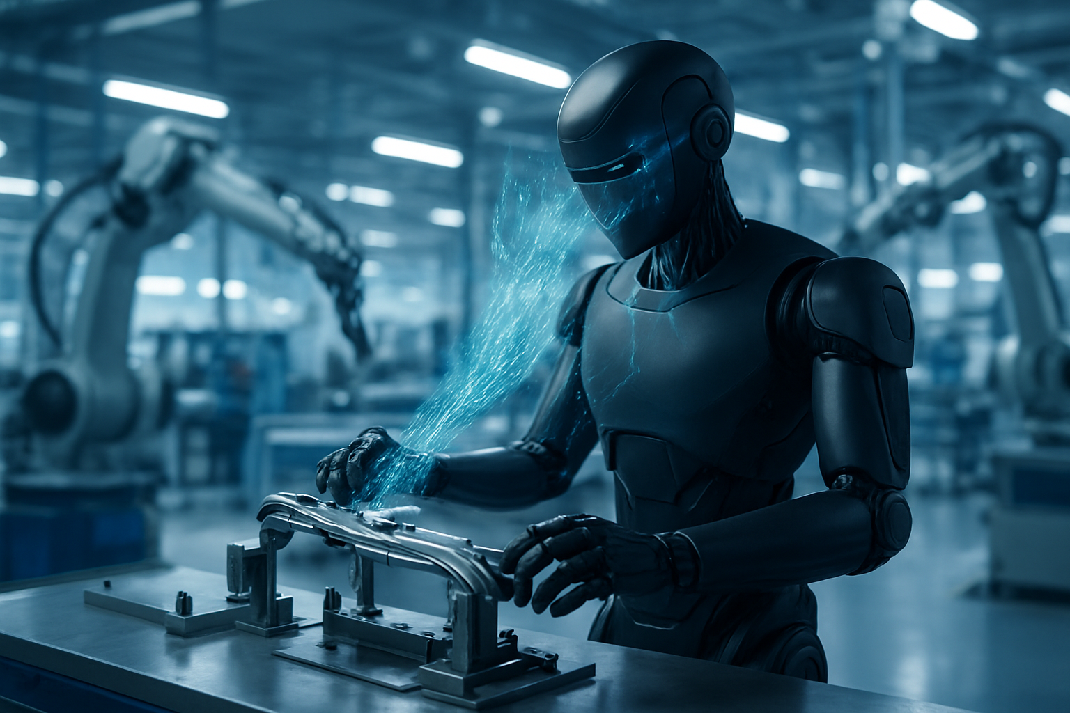
In a landmark shift for the robotics industry, Figure AI has successfully transitioned its humanoid platforms from experimental prototypes to functional industrial workers. By leveraging a groundbreaking end-to-end neural network architecture known as "Helix," the company’s latest robots—including the production-ready Figure 02 and the recently unveiled Figure 03—are now capable of mastering complex physical tasks simply by observing human demonstrations. This "watch-and-learn" capability has moved beyond simple laboratory tricks, such as making coffee, to high-stakes integration within global manufacturing hubs.
The significance of this development cannot be overstated. For decades, industrial robotics relied on rigid, pre-programmed movements that struggled with variability. Figure’s approach mirrors human cognition, allowing robots to interpret visual data and translate it into precise motor torques in real-time. As of late 2025, this technology is no longer a "future" prospect; it is currently being stress-tested on live production lines at the BMW Group (OTC: BMWYY) Spartanburg plant, marking the first time a general-purpose humanoid has maintained a multi-month operational streak in a heavy industrial setting.
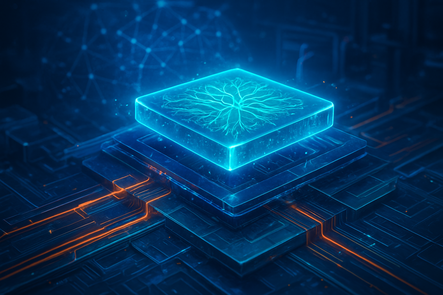
The Helix Architecture: A New Paradigm in Robotic Intelligence
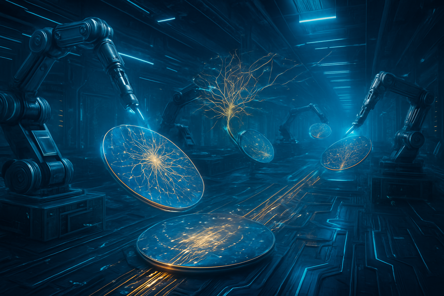
The technical backbone of Figure’s recent progress is the "Helix" Vision-Language-Action (VLA) model. Unlike previous iterations that relied on collaborative AI from partners like OpenAI, Figure moved its AI development entirely in-house in early 2025 to achieve tighter hardware-software integration. Helix utilizes a dual-system approach to mimic human thought: "System 2" provides high-level reasoning through a 7-billion parameter Vision-Language Model, while "System 1" operates as a high-frequency (200 Hz) visuomotor policy. This allows the robot to understand a command like "place the sheet metal on the fixture" while simultaneously making micro-adjustments to its grip to account for a slightly misaligned part.
This shift to end-to-end neural networks represents a departure from the modular "perception-planning-control" stacks of the past. In those older systems, an error in the vision module would cascade through the entire chain, often leading to total task failure. With Helix, the robot maps pixels directly to motor torque. This enables "imitation learning," where the robot watches video data of humans performing a task and builds a probabilistic model of how to replicate it. By mid-2025, Figure had scaled its training library to over 600 hours of high-quality human demonstration data, allowing its robots to generalize across tasks ranging from grocery sorting to complex industrial assembly without a single line of task-specific code.
The hardware has evolved in tandem with the intelligence. The Figure 02, which became the workhorse of the 2024-2025 period, features six onboard RGB cameras providing a 360-degree field of view and dual NVIDIA (NASDAQ: NVDA) RTX GPU modules for localized inference. Its hands, boasting 16 degrees of freedom and human-scale strength, allow it to handle delicate components and heavy tools with equal proficiency. The more recent Figure 03, introduced in October 2025, further refines this with integrated palm cameras and a lighter, more agile frame designed for the high-cadence environments of "BotQ," Figure's new mass-production facility.
Strategic Shifts and the Battle for the Factory Floor
The move to bring AI development in-house and terminate the OpenAI partnership was a strategic masterstroke that has repositioned Figure as a sovereign leader in the humanoid race. While competitors like Tesla (NASDAQ: TSLA) continue to refine the Optimus platform through internal vertical integration, Figure’s success with BMW has provided a "proof of utility" that few others can match. The partnership at the Spartanburg plant saw Figure robots operating for five consecutive months on the X3 body shop production line, achieving a 95% success rate in "bin-to-fixture" tasks. This real-world data is invaluable, creating a feedback loop that has already led to a 13% improvement in task speed through fleet-wide learning.
This development places significant pressure on other tech giants and AI labs. Microsoft (NASDAQ: MSFT) and Amazon (NASDAQ: AMZN), both major investors in Figure, stand to benefit immensely as they look to integrate these autonomous agents into their own logistics and cloud ecosystems. Conversely, traditional industrial robotics firms are finding their "single-purpose" arms increasingly threatened by the flexibility of Figure’s general-purpose humanoids. The ability to retrain a robot for a new task in a matter of hours via video demonstration—rather than weeks of manual programming—offers a competitive advantage that could disrupt the multi-billion dollar logistics and warehousing sectors.
Furthermore, the launch of "BotQ," Figure’s high-volume manufacturing facility in San Jose, signals the transition from R&D to commercial scale. Designed to produce 12,000 robots per year, BotQ is a "closed-loop" environment where existing Figure robots assist in the assembly of their successors. This self-sustaining manufacturing model is intended to drive down the cost per unit, making humanoid labor a viable alternative to traditional automation in a wider array of industries, including electronics assembly and even small-scale retail logistics.
The Broader Significance: General-Purpose AI Meets the Physical World
Figure’s progress marks a pivotal moment in the broader AI landscape, signaling the arrival of "Physical AI." While Large Language Models (LLMs) have mastered text and image generation, the "Moravec’s Paradox"—the idea that high-level reasoning is easy for AI but low-level sensorimotor skills are hard—has finally been challenged. By successfully mapping visual input to physical action, Figure has bridged the gap between digital intelligence and physical labor. This aligns with a broader trend in 2025 where AI is moving out of the browser and into the "real world" to address labor shortages in aging societies.
However, this rapid advancement brings a host of ethical and societal concerns. The ability for a robot to learn any task by watching a video suggests a future where human manual labor could be rapidly displaced across multiple sectors simultaneously. While Figure emphasizes that its robots are designed to handle "dull, dirty, and dangerous" jobs, the versatility of the Helix architecture means that even more nuanced roles could eventually be automated. Industry experts are already calling for updated safety standards and labor regulations to manage the influx of autonomous humanoids into public and private workspaces.
Comparatively, this milestone is being viewed by the research community as the "GPT-3 moment" for robotics. Just as GPT-3 demonstrated that scaling data and compute could lead to emergent linguistic capabilities, Figure’s work with imitation learning suggests that scaling visual demonstration data can lead to emergent physical dexterity. This shift from "programming" to "training" is the definitive breakthrough that will likely define the next decade of robotics, moving the industry away from specialized machines toward truly general-purpose assistants.
Looking Ahead: The Road to 100,000 Humanoids
In the near term, Figure is focused on scaling its deployment within the automotive sector. Following the success at BMW, several other major manufacturers are reportedly in talks to begin pilot programs in early 2026. The goal is to move beyond simple part-moving tasks into more complex assembly roles, such as wire harness installation and quality inspection using the Figure 03’s advanced palm cameras. Figure’s leadership has set an ambitious target of shipping 100,000 robots over the next four years, a goal that hinges on the continued success of the BotQ facility.
Long-term, the applications for Figure’s technology extend far beyond the factory. With the introduction of "soft-goods" coverings and enhanced safety protocols in the Figure 03 model, the company is clearly eyeing the domestic market. Experts predict that by 2027, we may see the first iterations of these robots entering home environments to assist with laundry, cleaning, and elder care. The primary challenge remains "edge-case" handling—ensuring the robot can react safely to unpredictable human behavior in unstructured environments—but the rapid iteration seen in 2025 suggests these hurdles are being cleared faster than anticipated.
A New Chapter in Human-Robot Collaboration
Figure AI’s achievements over the past year have fundamentally altered the trajectory of the robotics industry. By proving that a humanoid robot can learn complex tasks through visual observation and maintain a persistent presence in a high-intensity factory environment, the company has moved the conversation from "if" humanoids will be useful to "how quickly" they can be deployed. The integration of the Helix architecture and the success of the BMW partnership serve as a powerful validation of the end-to-end neural network approach.
As we look toward 2026, the key metrics to watch will be the production ramp-up at BotQ and the expansion of Figure’s fleet into new industrial verticals. The era of the general-purpose humanoid has officially arrived, and its impact on global manufacturing, logistics, and eventually daily life, is set to be profound. Figure has not just built a better robot; it has built a system that allows robots to learn, adapt, and work alongside humanity in ways that were once the sole province of science fiction.
This content is intended for informational purposes only and represents analysis of current AI developments.
TokenRing AI delivers enterprise-grade solutions for multi-agent AI workflow orchestration, AI-powered development tools, and seamless remote collaboration platforms.
For more information, visit https://www.tokenring.ai/.