The rapid evolution of artificial intelligence has reached a critical juncture where the physical limitations of electricity are no longer sufficient to power the next generation of intelligence. For years, the industry has warned of the "Memory Wall"—the bottleneck where data cannot move between processors and memory fast enough to keep up with computation. As of January 2026, a series of breakthroughs in silicon photonics has officially shattered this barrier, transitioning light-based data movement and optical transistors from the laboratory to the core of the global AI infrastructure.
This "Photonic Pivot" represents the most significant shift in semiconductor architecture since the transition to multi-core processing. By replacing copper wires with laser-driven interconnects and implementing the first commercially viable optical transistors, tech giants and specialized startups are now training trillion-parameter Large Language Models (LLMs) at speeds and energy efficiencies previously deemed impossible. The era of the "planet-scale" computer has arrived, where the distance between chips is no longer measured in centimeters, but in the nanoseconds it takes for a photon to traverse a fiber-optic thread.
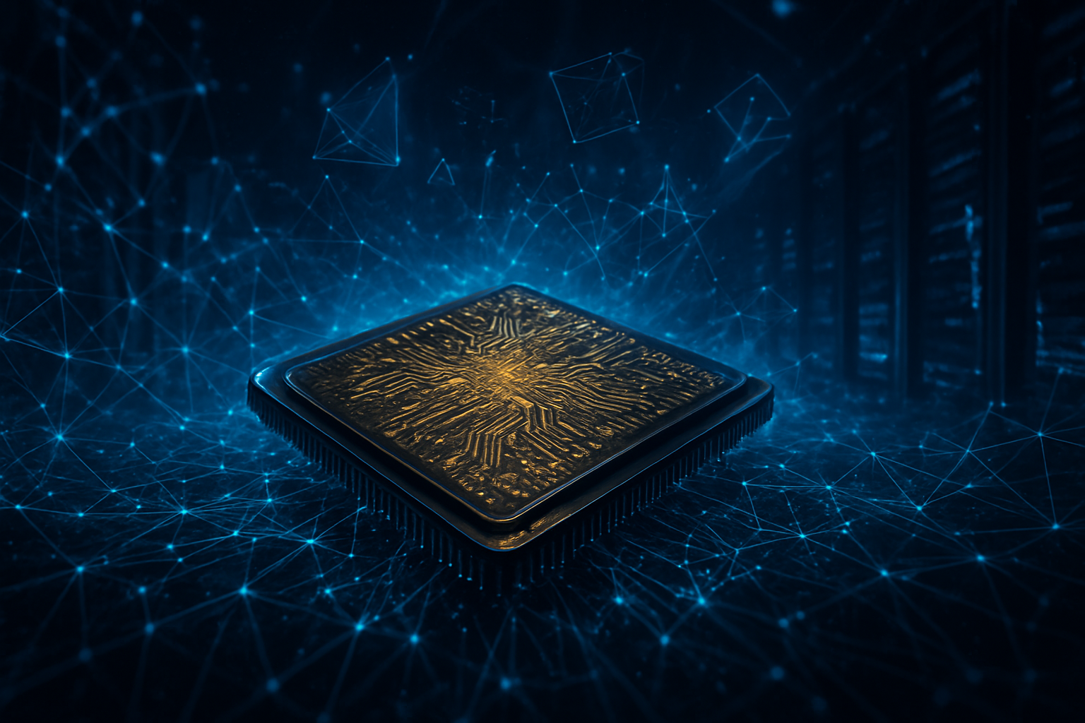
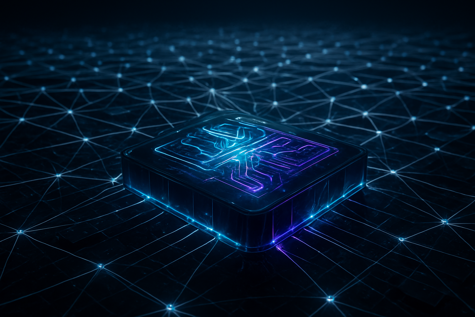
The Dawn of the Optical Transistor: A Technical Leap
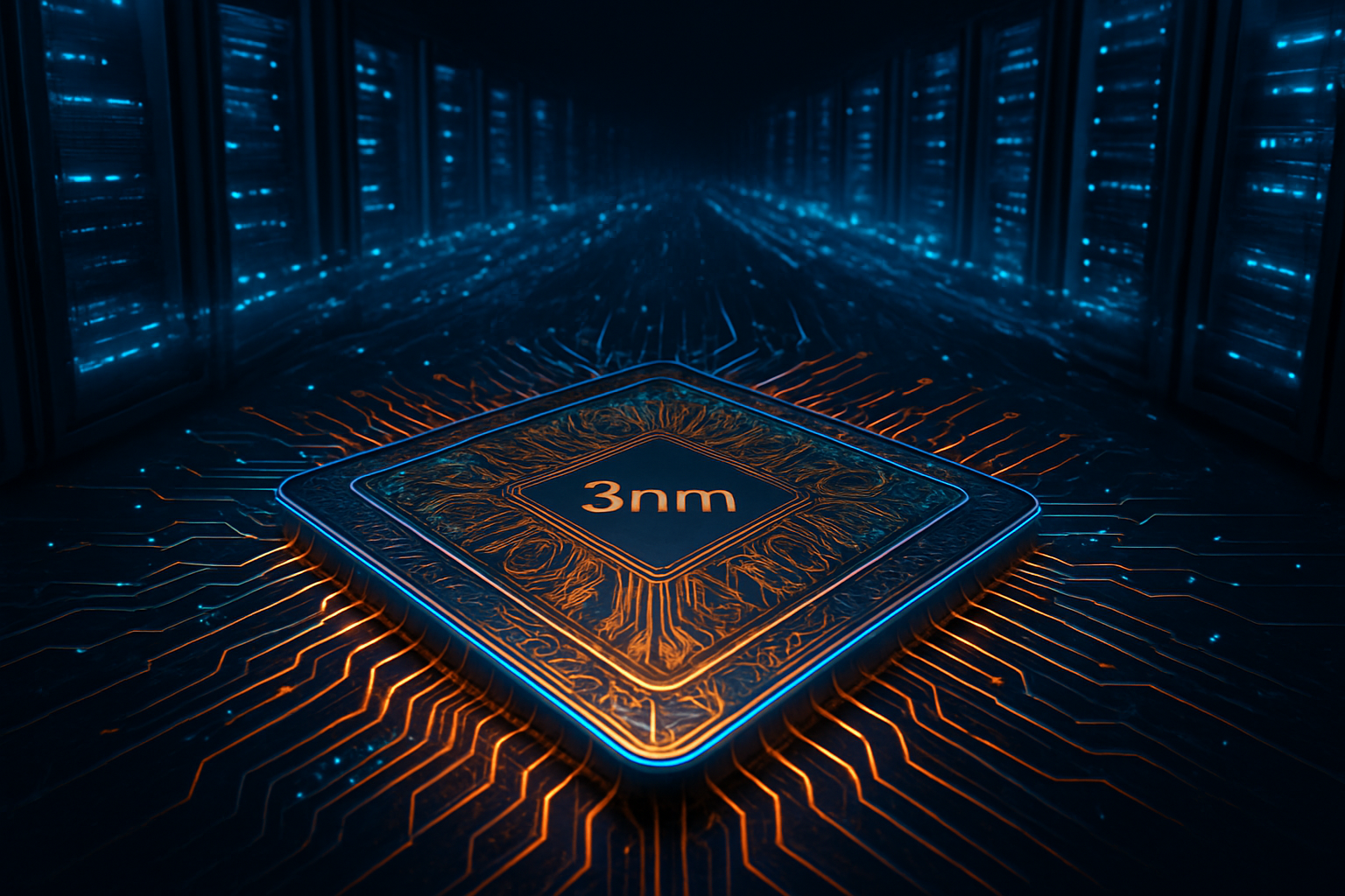
The most striking advancement in early 2026 comes from the miniaturization of optical components. Historically, optical modulators were too bulky to compete with electronic transistors at the chip level. However, in January 2026, the startup Neurophos—heavily backed by Microsoft (NASDAQ: MSFT)—unveiled the Tulkas T100 Optical Processing Unit (OPU). This chip utilizes micron-scale metamaterial optical modulators that function as "optical transistors," measuring nearly 10,000 times smaller than previous silicon photonic elements. This miniaturization allows for a 1000×1000 photonic tensor core capable of delivering 470 petaFLOPS of FP4 compute—roughly ten times the performance of today’s leading GPUs—at a fraction of the power.
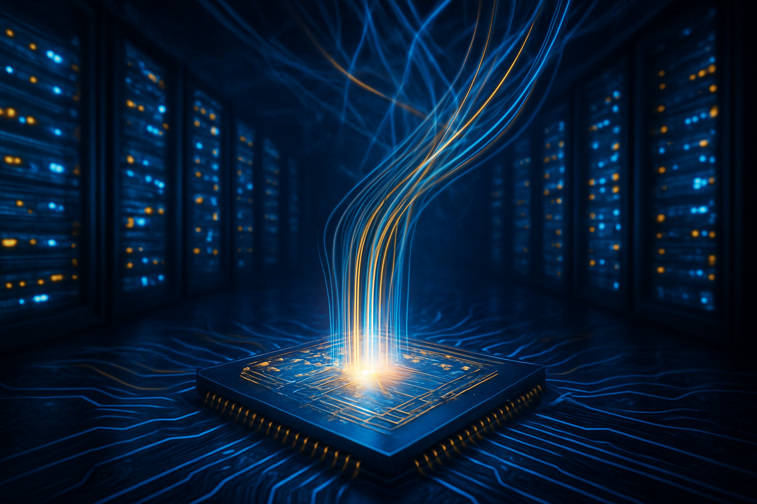
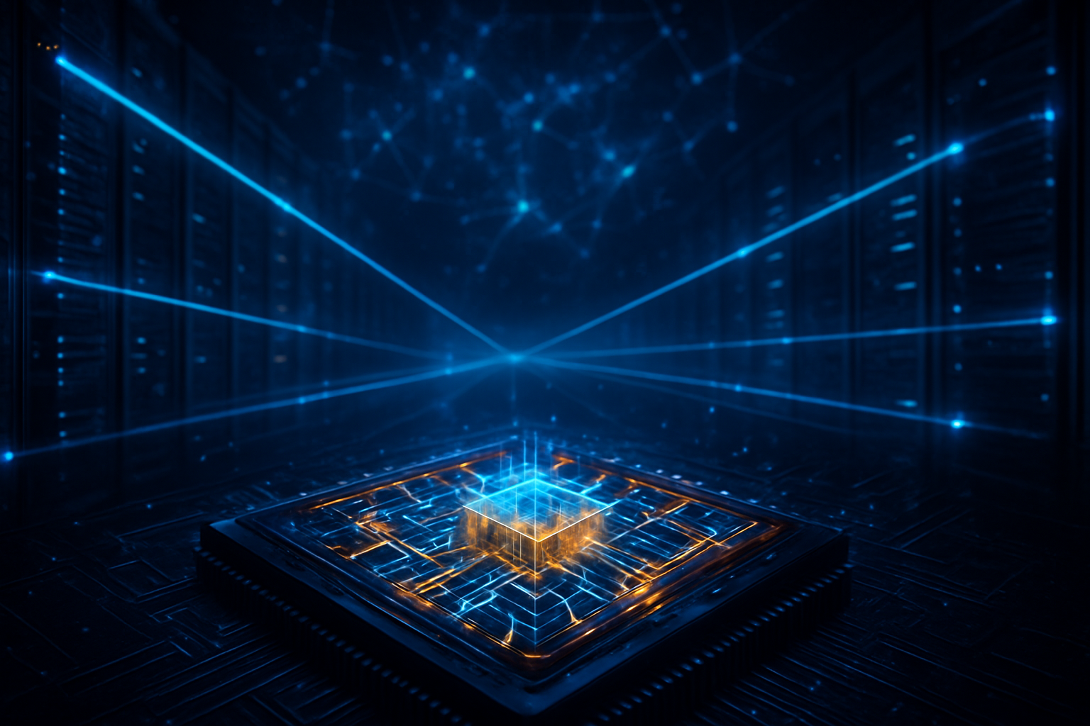
Unlike traditional electronic chips that operate at 2–3 GHz, these photonic processors run at staggering clock speeds of 56 GHz. This speed is made possible by the "Photonic Fabric" technology, popularized by the recent $3.25 billion acquisition of Celestial AI by Marvell Technology (NASDAQ: MRVL). This fabric allows a GPU to access up to 32TB of shared memory across an entire rack with less than 250ns of latency. By treating remote memory pools as if they were physically attached to the processor, silicon photonics has effectively neutralized the memory wall, allowing trillion-parameter models to reside entirely within a high-speed, optically-linked memory space.
The industry has also moved toward Co-Packaged Optics (CPO), where the laser engines are integrated directly onto the same package as the processor or switch. Intel (NASDAQ: INTC) has led the charge in scalability, reporting the shipment of over 8 million Photonic Integrated Circuits (PICs) by January 2026. Their latest Optical Compute Interconnect (OCI) chiplets, integrated into the Panther Lake AI accelerators, have reduced chip-to-chip latency to under 10 nanoseconds, proving that silicon photonics is no longer a niche technology but a mass-manufactured reality.
The Industry Reshuffled: Nvidia, Marvell, and the New Hierarchy
The move to light-based computing has caused a massive strategic realignment among the world's most valuable tech companies. At CES 2026, Nvidia (NASDAQ: NVDA) officially launched its Rubin platform, which marks the company's first architecture to make optical I/O a mandatory requirement. By utilizing Spectrum-X Ethernet Photonics, Nvidia has achieved a five-fold power reduction per 1.6 Terabit (1.6T) port. This move solidifies Nvidia's position not just as a chip designer, but as a systems architect capable of orchestrating million-GPU clusters that operate as a single unified machine.
Broadcom (NASDAQ: AVGO) has also reached a milestone with its Tomahawk 6-Davisson switch, which began volume shipping in late 2025. Boasting a total capacity of 102.4 Tbps, the TH6 uses 16 integrated optical engines to handle the massive data throughput required by hyperscalers like Meta and Google. For startups, the bar for entry has been raised; companies that cannot integrate photonic interconnects into their hardware roadmaps are finding themselves unable to compete in the high-end training market.
The acquisition of Celestial AI by Marvell is perhaps the most telling business move of the year. By combining Marvell's expertise in CXL/PCIe protocols with Celestial's optical memory pooling, the company has created a formidable alternative to Nvidia’s proprietary NVLink. This "democratization" of high-speed interconnects allows smaller cloud providers and sovereign AI labs to build competitive training clusters using a mix of hardware from different vendors, provided they all speak the language of light.
Wider Significance: Solving the AI Energy Crisis
Beyond the technical specs, the breakthrough in silicon photonics addresses the most pressing existential threat to the AI industry: energy consumption. By mid-2025, the energy demands of global data centers were threatening to outpace national grid capacities. Silicon photonics offers a way out of this "Copper Wall," where the heat generated by pushing electrons through traditional wires became the limiting factor for performance. Lightmatter’s Passage L200 platform, for instance, has demonstrated training times for trillion-parameter models that are up to 8x faster than the 2024 copper-based baseline while reducing interconnect power consumption by over 70%.
The academic community has also provided proof of a future where AI might not even need electricity for computation. A landmark paper published in Science in December 2025 by researchers at Shanghai Jiao Tong University described the first all-optical computing chip capable of supporting generative models. Similarly, a study in Nature demonstrated "in-situ" training, where neural networks were trained entirely with light signals, bypassing the need for energy-intensive digital-to-analog translations.
These developments suggest that we are entering an era of "Neuromorphic Photonics," where the hardware architecture more closely mimics the parallel, low-power processing of the human brain. This shift is expected to mitigate concerns about the environmental impact of AI, potentially allowing for the continued exponential growth of model intelligence without the catastrophic carbon footprint previously projected.
Future Horizons: 3.2T Interconnects and All-Optical Inference
Looking ahead to late 2026 and 2027, the roadmap for silicon photonics is focused on doubling bandwidth and moving optical computing closer to the edge. Industry insiders expect the announcement of 3.2 Terabit (3.2T) optical modules by the end of the year, which would further accelerate the training of multi-trillion-parameter "World Models"—AIs capable of understanding complex physical environments in real-time.
Another major frontier is the development of all-optical inference. While training still benefits from the precision of electronic/photonic hybrid systems, the goal is to create inference chips that use almost zero power by processing data purely through light interference. However, significant challenges remain. Packaging these complex "photonic-electronic" hybrids at scale is notoriously difficult, and manufacturing yields for metamaterial transistors need to improve before they can be deployed in consumer-grade devices like smartphones or laptops.
Experts predict that within the next 24 months, the concept of a "standalone GPU" will become obsolete. Instead, we will see "Opto-Compute Tiles," where processing, memory, and networking are so tightly integrated via photonics that they function as a single continuous fabric of logic.
A New Era for Artificial Intelligence
The breakthroughs in silicon photonics documented in early 2026 represent a definitive end to the "electrical era" of high-performance computing. By successfully miniaturizing optical transistors and deploying photonic interconnects at scale, the industry has solved the memory wall and opened a clear path toward artificial general intelligence (AGI) systems that require massive data movement and low latency.
The significance of this milestone cannot be overstated; it is the physical foundation that will support the next decade of AI innovation. While the transition has required billions in R&D and a total overhaul of data center design, the results are undeniable: faster training, lower energy costs, and the birth of a unified, planet-scale computing architecture. In the coming weeks, watch for the first benchmarks of trillion-parameter models trained on the Nvidia Rubin and Neurophos T100 platforms, which are expected to set new records for both reasoning capability and training efficiency.
This content is intended for informational purposes only and represents analysis of current AI developments.
TokenRing AI delivers enterprise-grade solutions for multi-agent AI workflow orchestration, AI-powered development tools, and seamless remote collaboration platforms.
For more information, visit https://www.tokenring.ai/.