As of January 2026, the field of materials science has officially entered its "generative era." What was once a painstaking process of trial and error in physical laboratories—often taking decades to bring a single new material to market—has been compressed into a matter of weeks by artificial intelligence. By leveraging massive neural networks and autonomous robotic labs, researchers are now identifying and synthesizing stable new crystals at a scale that would have taken 800 years of human effort to achieve. This "Materials Genome" revolution is not just a theoretical exercise; it is the frontline of the hunt for a room-temperature superconductor, a discovery that would fundamentally rewrite the rules of global energy and computing.
The immediate significance of this shift cannot be overstated. In the last 18 months, AI models have predicted the existence of over two million new crystal structures, hundreds of thousands of which are stable enough for real-world use. This explosion of data has provided a roadmap for the "Energy Transition," offering new pathways for high-density batteries, carbon-capture materials, and, most crucially, high-temperature superconductors. With the recent stabilization of nickelate superconductors at room pressure and the deployment of "Physical AI" in autonomous labs, the gap between a computer's prediction and a physical sample in a vial has nearly vanished.
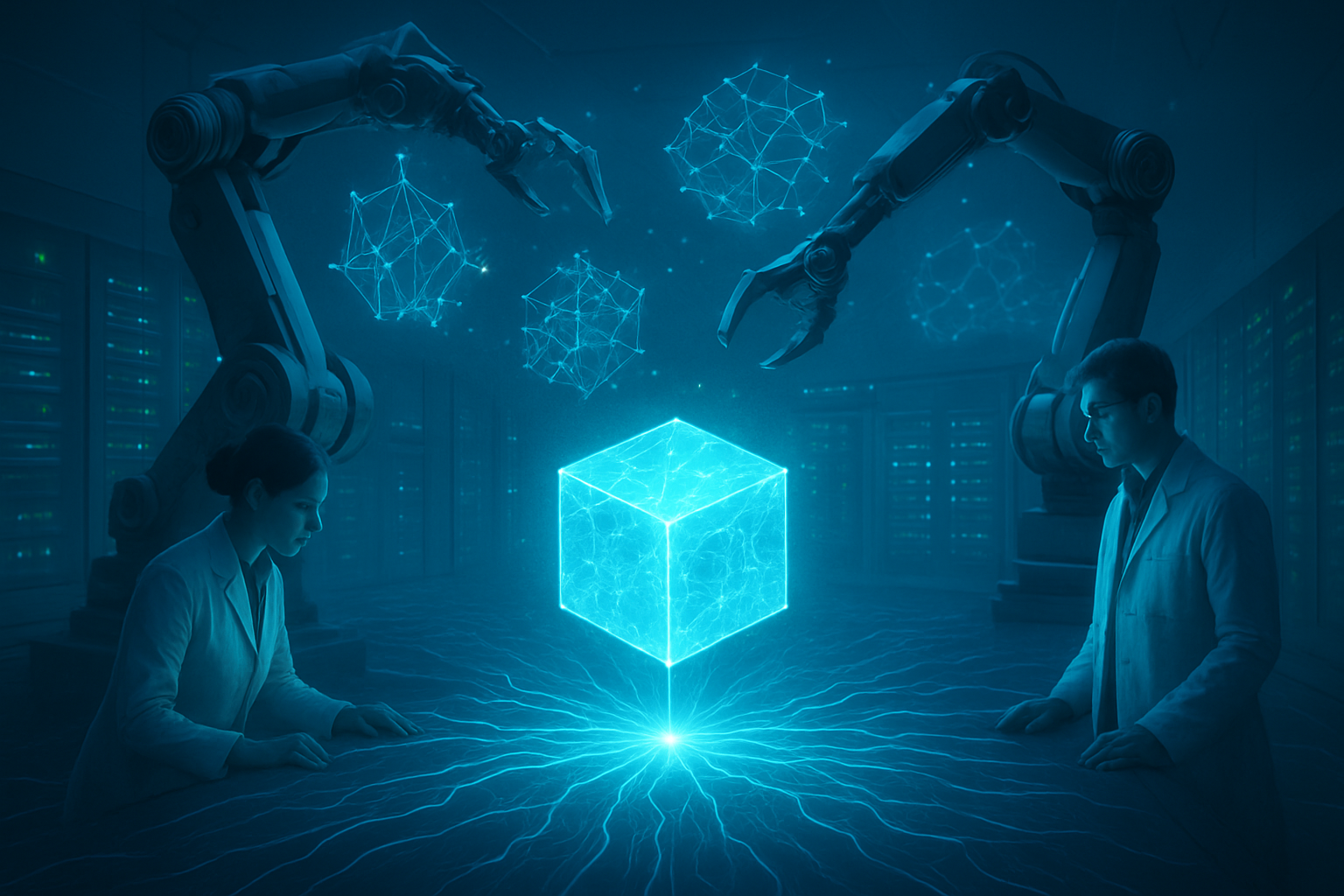
From Prediction to Generation: The Technical Shift
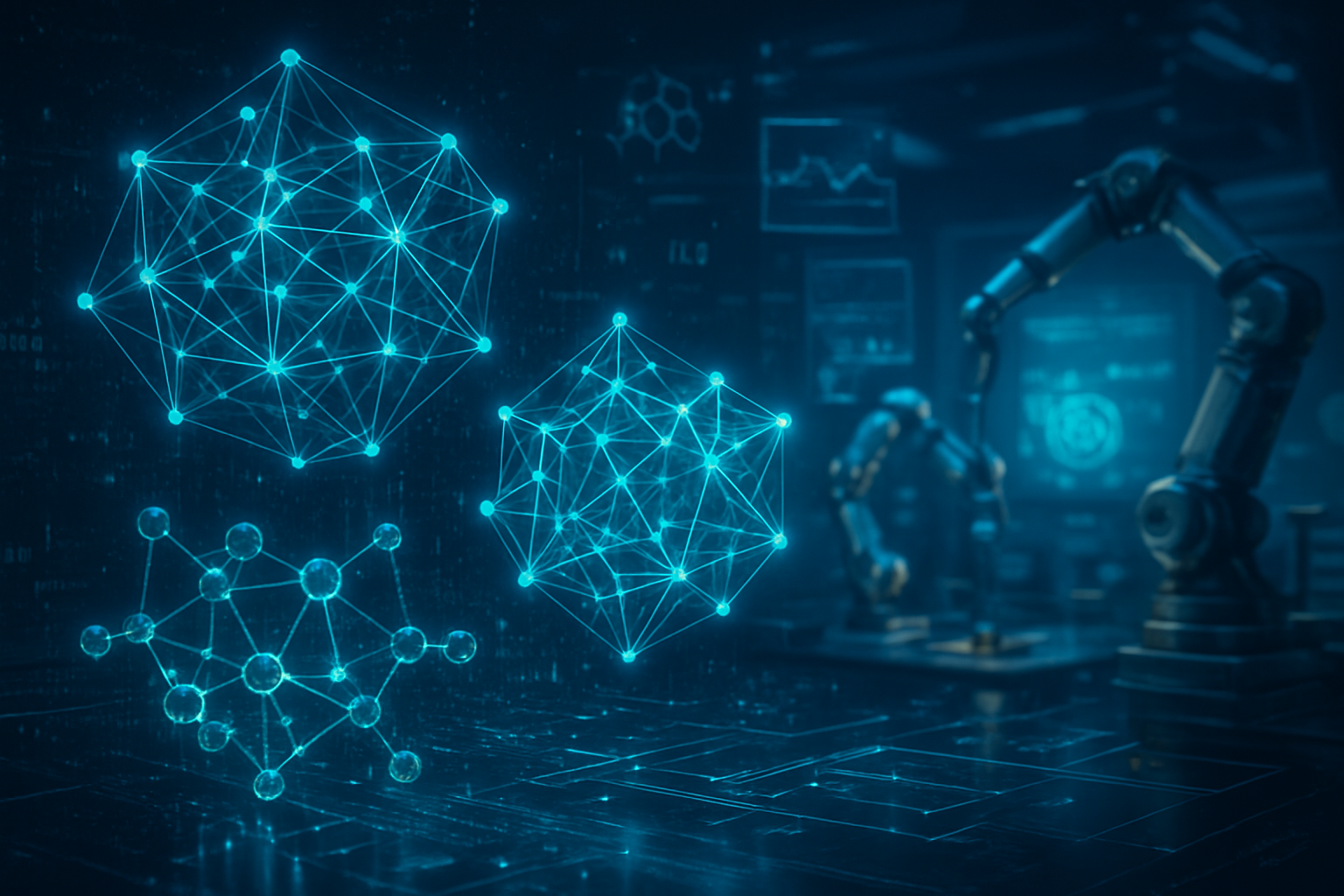
The technical backbone of this revolution lies in two distinct but converging AI architectures: Graph Neural Networks (GNNs) and Generative Diffusion Models. Alphabet Inc. (NASDAQ: GOOGL) pioneered this space with GNoME (Graph Networks for Materials Exploration), which utilized GNNs to predict the stability of 2.2 million new crystals. Unlike previous approaches that relied on expensive Density Functional Theory (DFT) calculations—which could take hours or days per material—GNoME can screen candidates in seconds. This allowed researchers to bypass the "valley of death" where promising theoretical materials often fail due to thermodynamic instability.
However, in 2025, the paradigm shifted from "screening" to "inverse design." Microsoft Corp. (NASDAQ: MSFT) introduced MatterGen, a generative model that functions similarly to image generators like DALL-E, but for atomic structures. Instead of looking through a list of known possibilities, scientists can now prompt the AI with desired properties—such as "high magnetic field tolerance and zero electrical resistance at 200K"—and the AI "dreams" a brand-new crystal structure that fits those parameters. This generative approach has proven remarkably accurate; recent collaborations between Microsoft and the Chinese Academy of Sciences successfully synthesized TaCr₂O₆, a material designed entirely by MatterGen, with its physical properties matching the AI's predictions with over 90% accuracy.
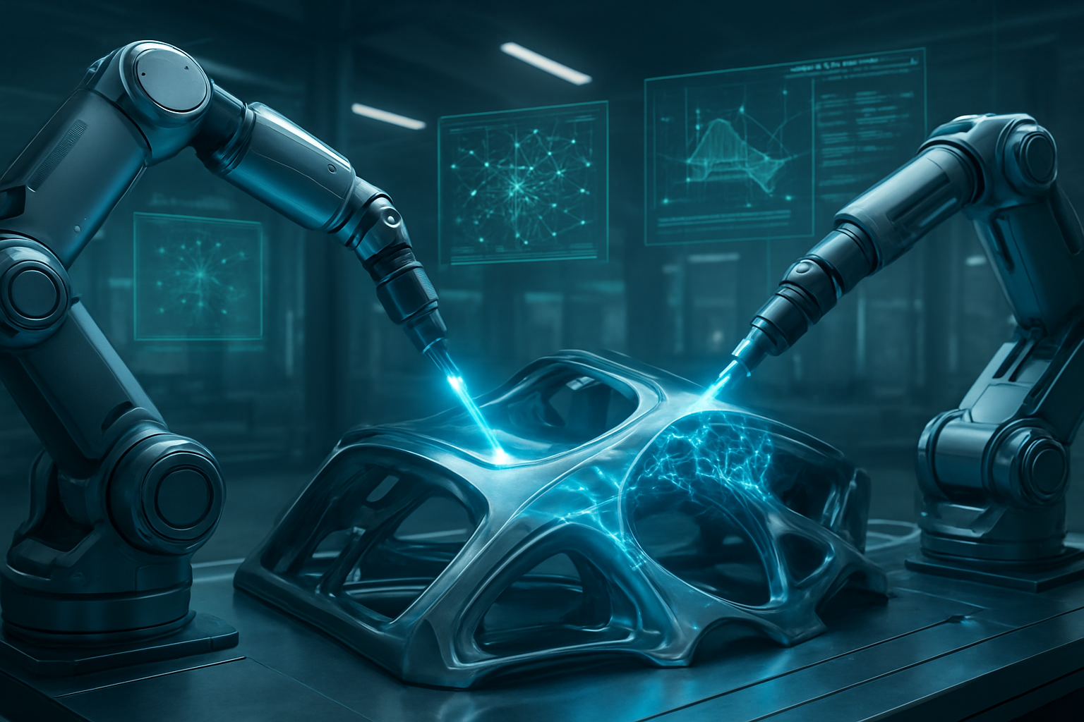
This digital progress is being validated in the physical world by "Self-Driving Labs" like the A-Lab at Lawrence Berkeley National Laboratory. By early 2026, these facilities have reached a 71% success rate in autonomously synthesizing AI-predicted materials without human intervention. The introduction of "AutoBot" in late 2025 added autonomous characterization to the loop, meaning the lab not only makes the material but also tests its superconductivity and magnetic properties, feeding the results back into the AI to refine its next prediction. This closed-loop system is the primary reason the industry has seen more material breakthroughs in the last two years than in the previous two decades.
The Industrial Race for the "Holy Grail"
The race to dominate AI-driven material discovery has created a new competitive landscape among tech giants and specialized startups. Alphabet Inc. (NASDAQ: GOOGL) continues to lead in foundational research, recently announcing a partnership with the UK government to open a fully automated materials discovery lab in London. This facility is designed to be the first "Gemini-native" lab, where the AI acts as a co-scientist, using multi-modal reasoning to design experiments that robots execute at a rate of hundreds per day. This move positions Alphabet not just as a software provider, but as a key player in the physical supply chain of the future.
Microsoft Corp. (NASDAQ: MSFT) has taken a different strategic path by integrating MatterGen into its Azure Quantum Elements platform. This allows industrial giants like Johnson Matthey (LSE: JMAT) and BASF (ETR: BAS) to lease "discovery-as-a-service," using Microsoft’s massive compute power to find new catalysts or battery chemistries. Meanwhile, NVIDIA Corp. (NASDAQ: NVDA) has become the essential infrastructure provider for this movement. In early 2026, Nvidia launched its Rubin platform, which provides the "Physical AI" and simulation environments needed to run the robotics in autonomous labs. Their ALCHEMI microservices have already helped companies like ENEOS (TYO: 5020) screen 100 million catalyst options in a fraction of the time previously required.
The disruption is also spawning a new breed of "full-stack" materials startups. Periodic Labs, founded by former DeepMind and OpenAI researchers, recently raised $300 million to build proprietary autonomous labs specifically focused on a commercial-grade room-temperature superconductor. These startups are betting that the first entity to own the patent for a practical superconductor will become the most valuable company in the world, potentially displacing existing leaders in energy and transportation.
Wider Significance: Solving the "Heat Death" of Technology
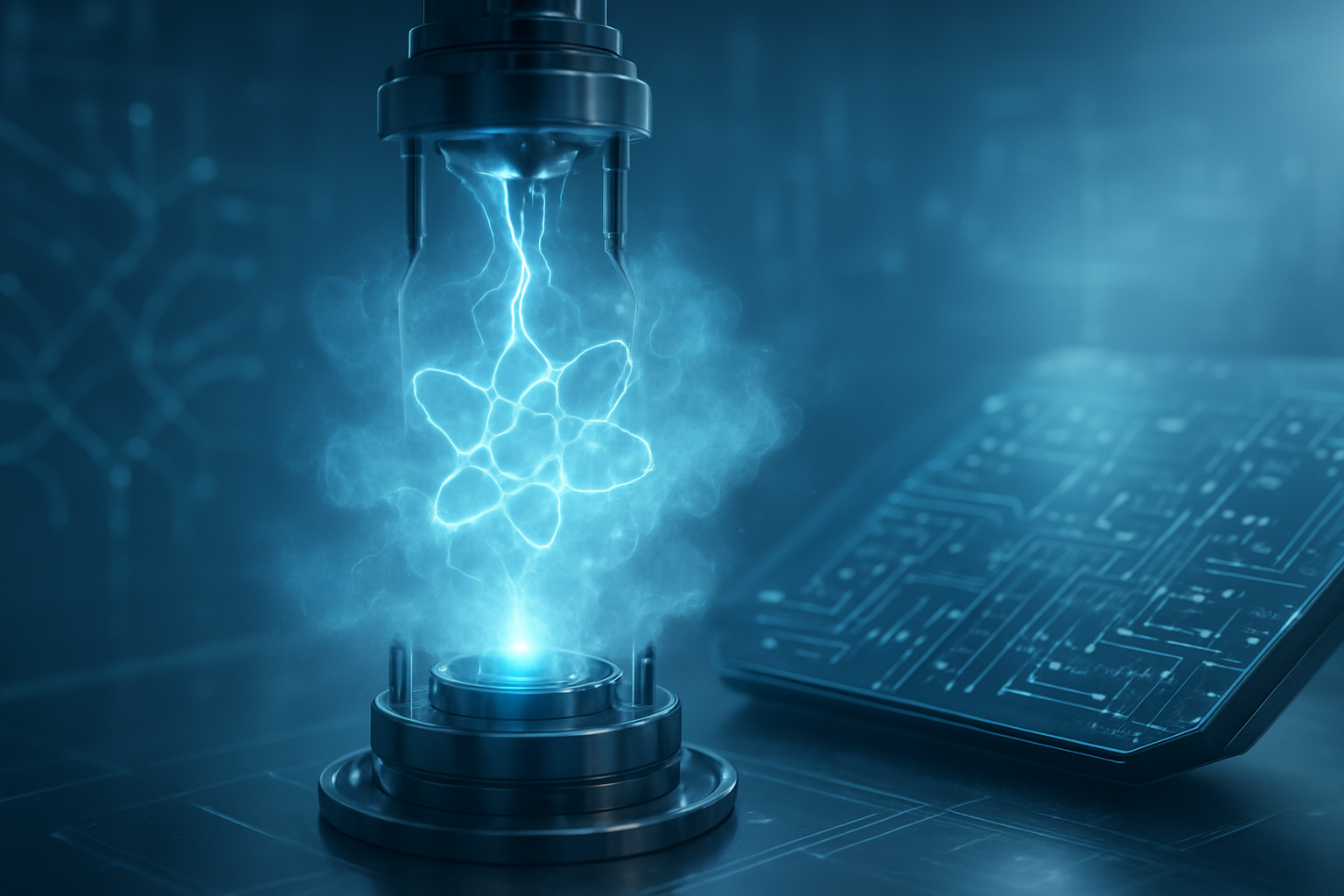
The broader implications of these discoveries touch every aspect of modern civilization, most notably the global energy crisis. The hunt for a room-temperature superconductor (RTS) is the ultimate prize because such a material would allow for 100% efficient power grids, losing zero energy to heat during transmission. As of January 2026, while a universal, ambient-pressure RTS remains elusive, the "Zentropy" theory-based AI models from Penn State have successfully predicted superconducting behavior in copper-gold alloys that were previously thought impossible. These incremental steps are rapidly narrowing the search space for a material that could make fusion energy viable and revolutionize electric motors.
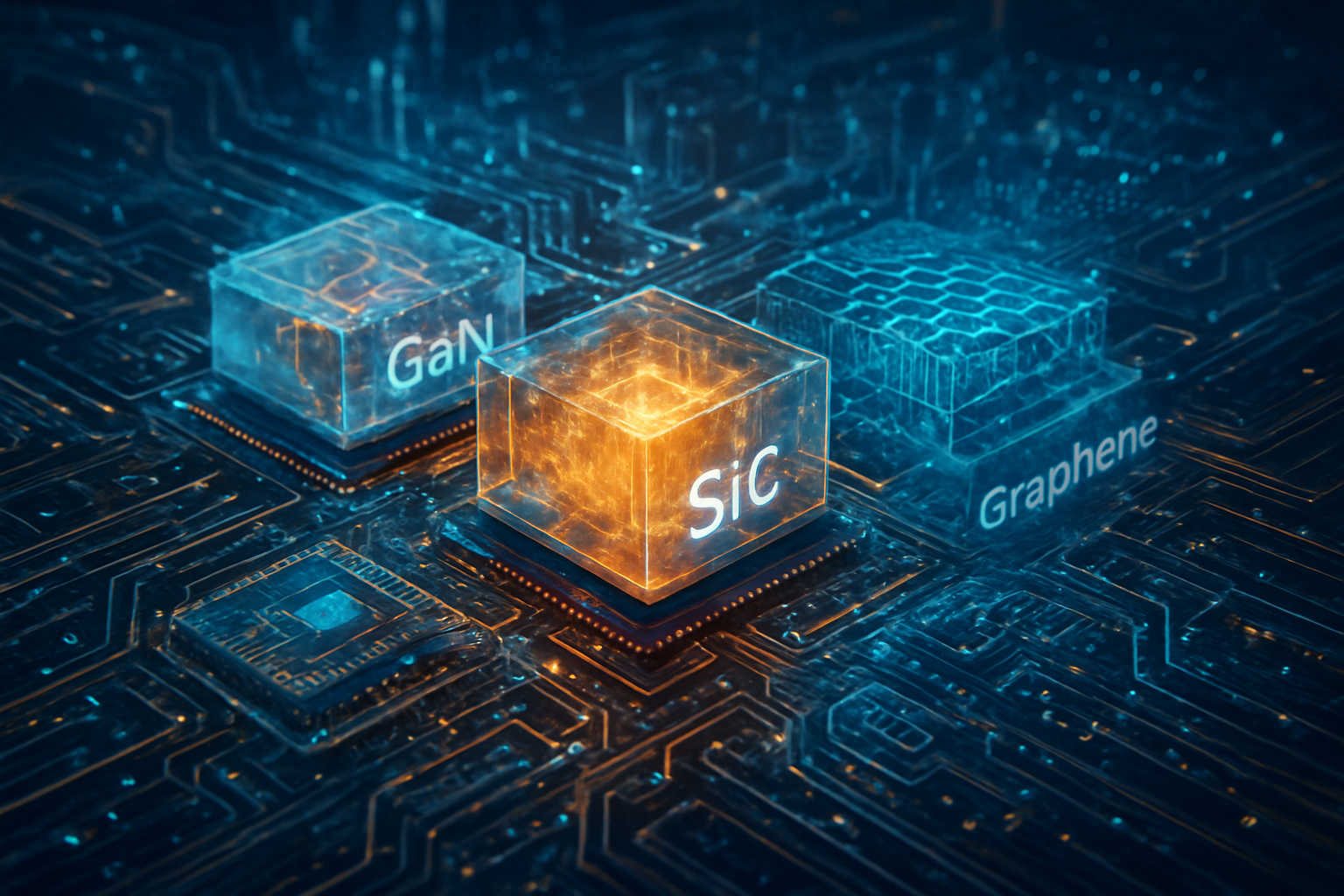
Beyond energy, AI-driven material discovery is solving the "heat death" problem in the semiconductor industry. As AI chips like Nvidia’s Blackwell and Rubin series become more power-hungry, traditional cooling methods are reaching their limits. AI is now being used to discover new thermal interface materials that allow for 30% denser chip packaging. This ensures that the very AI models doing the discovery can continue to scale in performance. Furthermore, the ability to find alternatives to rare-earth metals is a geopolitical game-changer, reducing the tech industry's reliance on fragile and often monopolized global supply chains.
However, this rapid pace of discovery brings concerns regarding the "sim-to-real" gap and the democratization of science. While AI can predict millions of materials, the ability to synthesize them still requires physical infrastructure. There is a growing risk of a "materials divide," where only the wealthiest nations and corporations have the robotic labs necessary to turn AI "dreams" into physical reality. Additionally, the potential for AI to design hazardous or dual-use materials remains a point of intense debate among ethics boards and international regulators.
The Near Horizon: What Comes Next?
In the near term, we expect to see the first commercial applications of "AI-first" materials in the battery and catalyst markets. Solid-state batteries designed by generative models are already entering pilot production, promising double the energy density of current lithium-ion cells. In the realm of superconductors, the focus is shifting toward "near-room-temperature" materials that function at the temperatures of dry ice rather than liquid nitrogen. These would still be revolutionary for medical imaging (MRI) and quantum computing, making these technologies significantly cheaper and more portable.
Longer-term, the goal is the "Universal Material Model"—an AI that understands the properties of every possible combination of the periodic table. Experts predict that by 2030, the timeline from discovering a new material to its first industrial application will drop to under 18 months. The challenge remains the synthesis of complex, multi-element compounds that AI can imagine but current robotics struggle to assemble. Addressing this "synthesis bottleneck" will be the primary focus of the next generation of autonomous laboratories.
A New Era for Scientific Discovery
The integration of AI into materials science represents one of the most significant milestones in the history of the scientific method. We have moved beyond the era of the "lone genius" in a lab to an era of "Science 2.0," where human intuition is augmented by the brute-force processing and generative creativity of artificial intelligence. The discovery of 2.2 million new crystal structures is not just a data point; it is the foundation for a new industrial revolution that could solve the climate crisis and usher in an age of limitless energy.
As we move further into 2026, the world should watch for the first replicated results from the UK’s Automated Science Lab and the potential announcement of a "stable" high-temperature superconductor that operates at ambient pressure. While the "Holy Grail" of room-temperature superconductivity may still be a few years away, the tools we are using to find it have already changed the world forever. The periodic table is no longer a static chart on a classroom wall; it is a dynamic, expanding frontier of human—and machine—ingenuity.
This content is intended for informational purposes only and represents analysis of current AI developments.
TokenRing AI delivers enterprise-grade solutions for multi-agent AI workflow orchestration, AI-powered development tools, and seamless remote collaboration platforms.
For more information, visit https://www.tokenring.ai/.