Tag: Materials Science

  • Beyond Silicon: Photonics and Advanced Materials Forge the Future of Semiconductors

    Beyond Silicon: Photonics and Advanced Materials Forge the Future of Semiconductors

    The semiconductor industry stands at the precipice of a transformative era, driven by groundbreaking advancements in photonics and materials science. As traditional silicon-based technologies approach their physical limits, innovations in harnessing light and developing novel materials are emerging as critical enablers for the next generation of computing, communication, and artificial intelligence (AI) systems. These developments promise not only to overcome current bottlenecks but also to unlock unprecedented levels of performance, energy efficiency, and manufacturing capabilities, fundamentally reshaping the landscape of high-tech industries.

    This convergence of disciplines is poised to redefine what's possible in microelectronics. From ultra-fast optical interconnects that power hyperscale data centers to exotic two-dimensional materials enabling atomic-scale transistors and wide bandgap semiconductors revolutionizing power management, these fields are delivering the foundational technologies necessary to meet the insatiable demands of an increasingly data-intensive and AI-driven world. The immediate significance lies in their potential to dramatically accelerate data processing, reduce power consumption, and enable more compact and powerful devices across a myriad of applications.

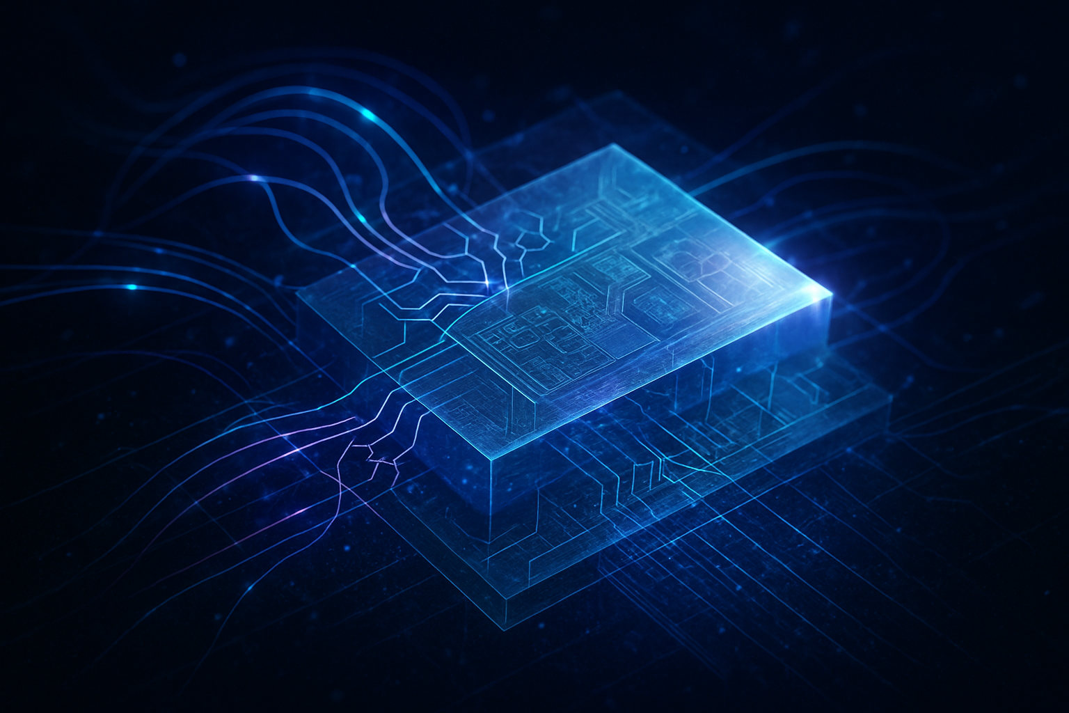
    The Technical Crucible: Light and Novel Structures Redefine Chip Architecture

    The core of this revolution lies in specific technical breakthroughs that challenge the very fabric of conventional semiconductor design. Silicon Photonics (SiP) is leading the charge, integrating optical components directly onto silicon chips using established CMOS manufacturing processes. This allows for ultra-fast interconnects, supporting data transmission speeds exceeding 800 Gbps, which is vital for bandwidth-hungry applications in data centers, cloud infrastructure, and 5G/6G networks. Crucially, SiP offers superior energy efficiency compared to traditional electronic interconnects, significantly curbing the power consumption of massive computing infrastructures. The market for silicon photonics is experiencing robust growth, with projections estimating it could reach USD 9.65 billion by 2030, reflecting its pivotal role in future communication.

    Further enhancing photonic integration, researchers have recently achieved a significant milestone with the development of the first electrically pumped continuous-wave semiconductor laser made entirely from Group IV elements (silicon-germanium-tin and germanium-tin) directly grown on a silicon wafer. This breakthrough addresses a long-standing challenge by paving the way for fully integrated photonic circuits without relying on off-chip light sources. Complementing this, Quantum Photonics is rapidly advancing, utilizing nano-sized semiconductor "quantum dots" as on-demand single-photon generators for quantum optical circuits. These innovations are fundamental for scalable quantum information processing, spanning secure communication, advanced sensing, and quantum computing, pushing beyond classical computing paradigms.

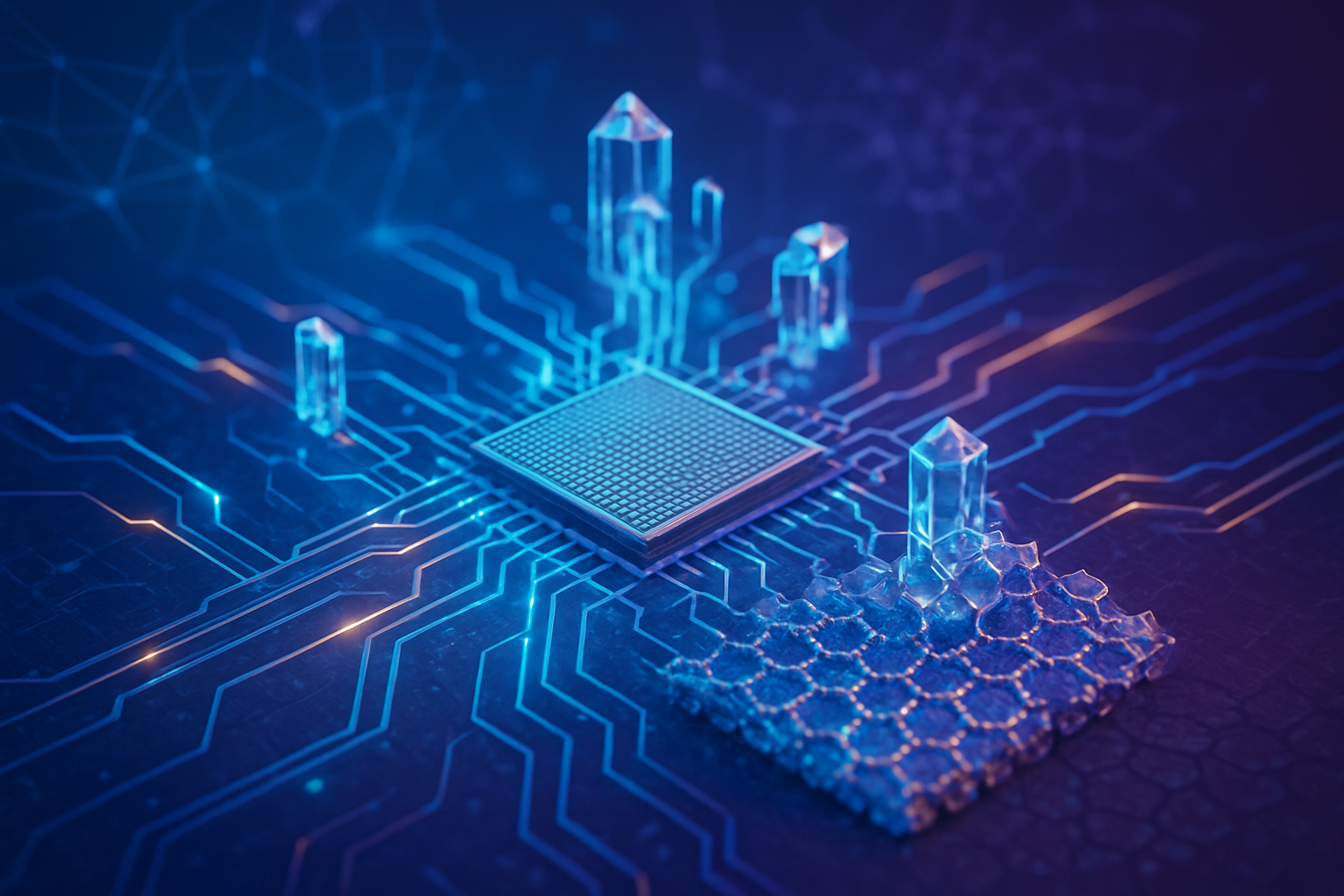
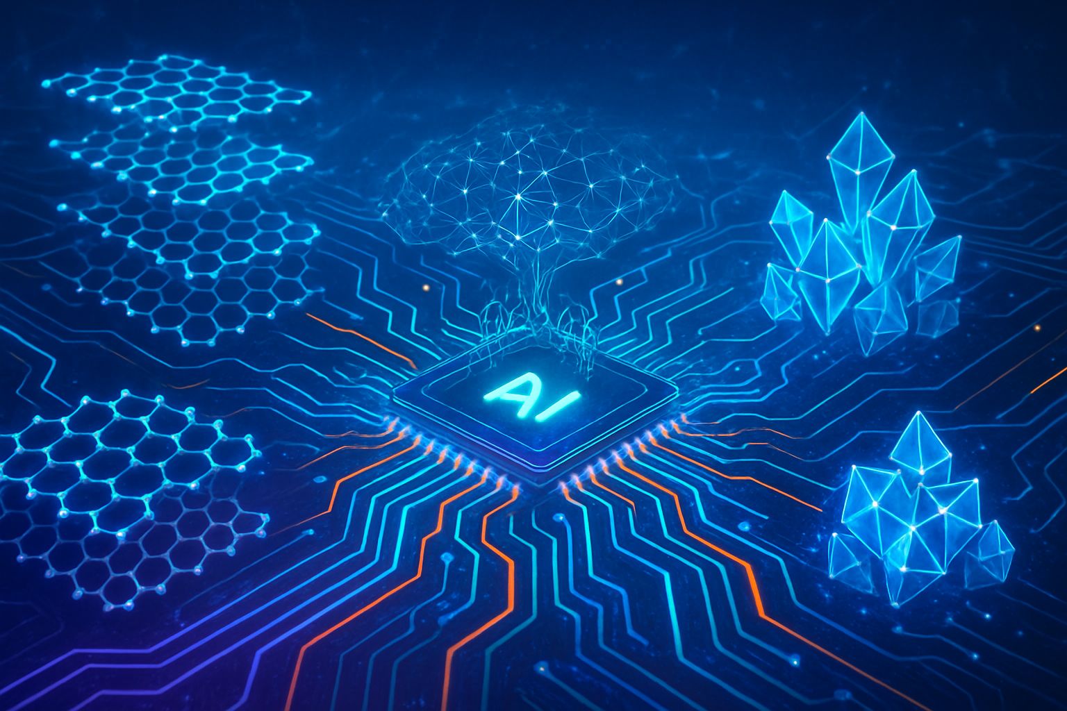
    On the materials science front, 2D Materials like graphene, molybdenum disulfide (MoS2), and hexagonal Boron Nitride (h-BN) are emerging as formidable contenders to or complements for silicon. These atomically thin materials boast exceptional electrical and thermal conductivity, mechanical strength, flexibility, and tunable bandgaps, enabling the creation of atomic-thin channel transistors and monolithic 3D integration. This allows for further miniaturization beyond silicon's physical limits while also improving thermal management and energy efficiency. Major industry players such as Taiwan Semiconductor Manufacturing Company (TSMC) (TWSE: 2330), Intel Corporation (NASDAQ: INTC), and IMEC are heavily investing in research and integration of these materials, recognizing their potential to unlock unprecedented performance and density.

    Another critical area is Wide Bandgap (WBG) Semiconductors, specifically Gallium Nitride (GaN) and Silicon Carbide (SiC). These materials offer superior performance over silicon, including higher breakdown voltages, improved thermal stability, and enhanced efficiency at high frequencies and power levels. They are indispensable for power electronics in electric vehicles, 5G infrastructure, renewable energy systems, and industrial machinery, contributing to extended battery life and reduced charging times. The global WBG semiconductor market is expanding rapidly, projected to grow from USD 2.13 billion in 2024 to USD 8.42 billion by 2034, underscoring their crucial role in modern power management. The integration of Artificial Intelligence (AI) in materials discovery and manufacturing processes further accelerates these advancements, with AI-driven simulation tools drastically reducing R&D cycles and optimizing design efficiency and yield in fabrication facilities for sub-2nm nodes.

    Corporate Battlegrounds: Reshaping the AI and Semiconductor Landscape

    The profound advancements in photonics and materials science are not merely technical curiosities; they are potent catalysts reshaping the competitive landscape for major AI companies, tech giants, and innovative startups. These innovations are critical for overcoming the limitations of current electronic systems, enabling the continued growth and scaling of AI, and will fundamentally redefine strategic advantages in the high-stakes world of AI hardware.

    NVIDIA Corporation (NASDAQ: NVDA), a dominant force in AI GPUs, is aggressively adopting silicon photonics to supercharge its next-generation AI clusters. The company is transitioning from pluggable optical modules to co-packaged optics (CPO), integrating optical engines directly with switch ASICs, which is projected to yield a 3.5x improvement in power efficiency, a 64x boost in signal integrity, and tenfold enhanced network resiliency, drastically accelerating system deployment. NVIDIA's upcoming Quantum-X and Spectrum-X Photonics switches, slated for launch in 2026, will leverage CPO for InfiniBand and Ethernet networks to connect millions of GPUs. By embedding photonic switches into its GPU-centric ecosystem, NVIDIA aims to solidify its leadership in AI infrastructure, offering comprehensive solutions for the burgeoning "AI factories" and effectively addressing data transmission bottlenecks that plague large-scale AI deployments.

    Intel Corporation (NASDAQ: INTC), a pioneer in silicon photonics, continues to invest heavily in this domain. It has introduced fully integrated optical compute interconnect (OCI) chiplets to revolutionize AI data transmission, boosting machine learning workload acceleration and mitigating electrical I/O limitations. Intel is also exploring optical neural networks (ONNs) with theoretical latency and power efficiency far exceeding traditional silicon designs. Intel’s ability to integrate indium phosphide-based lasers directly onto silicon chips at scale provides a significant advantage, positioning the company as a leader in energy-efficient AI at both the edge and in data centers, and intensifying its competition with NVIDIA and Advanced Micro Devices, Inc. (NASDAQ: AMD). However, the growing patent activity from Taiwan Semiconductor Manufacturing Company (TSMC) (TWSE: 2330) in silicon photonics suggests an escalating competitive dynamic.

    Advanced Micro Devices, Inc. (NASDAQ: AMD) is making bold strategic moves into silicon photonics, notably through its acquisition of the startup Enosemi. Enosemi's expertise in photonic integrated circuits (PICs) will enable AMD to develop co-packaged optics solutions for faster, more efficient data movement within server racks, a critical requirement for ever-growing AI models. This acquisition strategically positions AMD to compete more effectively with NVIDIA by integrating photonics into its full-stack AI portfolio, encompassing CPUs, GPUs, FPGAs, networking, and software. AMD is also collaborating with partners to define an open photonic interface standard, aiming to prevent proprietary lock-in and enable scalable, high-bandwidth interconnects for AI and high-performance computing (HPC).

    Meanwhile, tech giants like Google LLC (NASDAQ: GOOGL) and Microsoft Corporation (NASDAQ: MSFT) stand to benefit immensely from these advancements. As a major AI and cloud provider, Google's extensive use of AI for machine learning, natural language processing, and computer vision means it will be a primary customer for these advanced semiconductor technologies, leveraging them in its custom AI accelerators (like TPUs) and cloud infrastructure to offer superior AI services. Microsoft is actively researching and developing analog optical computers (AOCs) as a potential solution to AI’s growing energy crisis, with prototypes demonstrating up to 100 times greater energy efficiency for AI inference tasks than current GPUs. Such leadership in AOC development could furnish Microsoft with a unique, highly energy-efficient hardware platform, differentiating its Azure cloud services and potentially disrupting the dominance of existing GPU architectures.

    Taiwan Semiconductor Manufacturing Company (TSMC) (TWSE: 2330), as the world's largest contract chipmaker, is a critical enabler of these advancements. TSMC is heavily investing in silicon photonics to boost performance and energy efficiency for AI applications, targeting production readiness by 2029. Its COUPE platform for co-packaged optics is central to NVIDIA's future AI accelerator designs, and TSMC is also aggressively advancing in 2D materials research. TSMC's leadership in advanced fabrication nodes (3nm, 2nm, 1.4nm) and its aggressive push in silicon photonics solidify its position as the leading foundry for AI chips, making its ability to integrate these complex innovations a key competitive differentiator for its clientele.

    Beyond the giants, these innovations create fertile ground for emerging startups specializing in niche AI hardware, custom ASICs for specific AI tasks, or innovative cooling solutions. Companies like Lightmatter are developing optical chips that offer ultra-high speed, low latency, and low power consumption for HPC tasks. These startups act as vital innovation engines, developing specialized hardware that challenges traditional architectures and often become attractive acquisition targets for tech giants seeking to integrate cutting-edge photonics and materials science expertise, as exemplified by AMD's acquisition of Enosemi. The overall shift is towards heterogeneous integration, where diverse components like photonic and electronic elements are combined using advanced packaging, challenging traditional CPU-SRAM-DRAM architectures and giving rise to "AI factories" that demand a complete reinvention of networking infrastructure.

    A New Era of Intelligence: Broader Implications and Societal Shifts

    The integration of photonics and advanced materials science into semiconductor technology represents more than just an incremental upgrade; it signifies a fundamental paradigm shift with profound implications for the broader AI landscape and society at large. These innovations are not merely sustaining the current "AI supercycle" but are actively driving it, addressing the insatiable computational demands of generative AI and large language models (LLMs) while simultaneously opening doors to entirely new computing paradigms.

    At its core, this hardware revolution is about overcoming the physical limitations that have begun to constrain traditional silicon-based chips. As transistors shrink, quantum tunneling effects and the "memory wall" bottleneck—the slow data transfer between processor and memory—become increasingly problematic. Photonics and novel materials directly tackle these issues by enabling faster data movement with significantly less energy and by offering alternative computing architectures. For instance, photonic AI accelerators promise two orders of magnitude speed increase and three orders of magnitude reduction in power consumption for certain AI tasks compared to electronic counterparts. This dramatic increase in energy efficiency is critical, as the energy consumption of AI data centers is a growing concern, projected to double by the end of the decade, aligning with broader trends towards green computing and sustainable AI development.

    The societal impacts of these advancements are far-reaching. In healthcare, faster and more accurate AI will revolutionize diagnostics, enabling earlier disease detection (e.g., cancer) and personalized treatment plans based on genetic information. Wearable photonics with integrated AI functions could facilitate continuous health monitoring. In transportation, real-time, low-latency AI processing at the edge will enhance safety and responsiveness in autonomous systems like self-driving cars. For communication and data centers, silicon photonics will lead to higher density, performance, and energy efficiency, forming the backbone for the massive data demands of generative AI and LLMs. Furthermore, AI itself is accelerating the discovery of new materials with exotic properties for quantum computing, energy storage, and superconductors, promising to revolutionize various industries. By significantly reducing the energy footprint of AI, these advancements also contribute to environmental sustainability, mitigating concerns about carbon emissions from large-scale AI models.

    However, this transformative period is not without its challenges and concerns. The increasing sophistication of AI, powered by this advanced hardware, raises questions about job displacement in industries with repetitive tasks and significant ethical considerations regarding surveillance, facial recognition, and autonomous decision-making. Ensuring that advanced AI systems remain accessible and affordable during this transition is crucial to prevent a widening technological gap. Supply chain vulnerabilities and geopolitical tensions are also exacerbated by the global race for advanced semiconductor technology, leading to increased national investments in domestic fabrication capabilities. Technical hurdles, such as seamlessly integrating photonics and electronics and ensuring computational precision for large ML models, also need to be overcome. The photonics industry faces a growing skills gap, which could delay innovation, and despite efficiency gains, the sheer growth in AI model complexity means that overall energy demands will remain a significant concern.

    Comparing this era to previous AI milestones, the current hardware revolution is akin to, and in some ways surpasses, the transformative shift from CPU-only computing to GPU-accelerated AI. Just as GPUs propelled deep learning from an academic curiosity to a mainstream technology, these new architectures have the potential to spark another explosion of innovation, pushing AI into domains previously considered computationally infeasible. Unlike earlier AI milestones characterized primarily by algorithmic breakthroughs, the current phase is marked by the industrialization and scaling of AI, where specialized hardware is not just facilitating advancements but is often the primary bottleneck and key differentiator for progress. This shift signifies a move from simply optimizing existing architectures to fundamentally rethinking the very physics of computation for AI, ushering in a "post-transistor" era where AI not only consumes advanced chips but actively participates in their creation, optimizing chip design and manufacturing processes in a symbiotic "AI supercycle."

    The Road Ahead: Future Developments and the Dawn of a New Computing Paradigm

    The horizon for semiconductor technology, driven by photonics and advanced materials science, promises a "hardware renaissance" that will fundamentally redefine the capabilities of future intelligent systems. Both near-term and long-term developments point towards an era of unprecedented speed, energy efficiency, and novel computing architectures that will fuel the next wave of AI innovation.

    In the near term (1-5 years), we can expect to see the early commercial deployment of photonic AI chips in data centers, particularly for specialized high-speed, low-power AI inference tasks. Companies like Lightmatter, Lightelligence, and Celestial AI are at the forefront of this, with prototypes already being tested by tech giants like Microsoft (NASDAQ: MSFT) in their cloud data centers. These chips, which use light pulses instead of electrical signals, offer significantly reduced energy consumption and higher data rates, directly addressing the growing energy demands of AI. Concurrently, advancements in advanced lithography, such as ASML's High-NA EUV system, are expected to enable 2nm and 1.4nm process nodes by 2025, leading to more powerful and efficient AI accelerators and CPUs. The increased integration of novel materials like 2D materials (e.g., graphene in optical microchips, consuming 80% less energy than silicon photonics) and ferroelectric materials for ultra-low power memory solutions will become more prevalent. Wide Bandgap (WBG) semiconductors like GaN and SiC will further solidify their indispensable role in energy-intensive AI data centers due to their superior properties. The industry will also witness a growing emphasis on heterogeneous integration and advanced packaging, moving away from monolithic scaling to combine diverse functionalities onto single, dense modules through strategic partnerships.

    Looking further ahead into the long term (5-10+ years), the vision extends to a "post-silicon era" beyond 2027, with the widespread commercial integration of 2D materials for ultra-efficient transistors. The dream of all-optical compute and neuromorphic photonics—chips mimicking the human brain's structure and function—will continue to progress, offering ultra-efficient processing by utilizing phase-change materials for in-memory compute to eliminate the optical/electrical overhead of data movement. Miniaturization will reach new heights, with membrane-based nanophotonic technologies enabling tens of thousands of photonic components per chip, alongside optical modulators significantly smaller than current silicon-photonic devices. A profound prediction is the continuous, symbiotic evolution where AI tools will increasingly design their own chips, accelerate development, and even discover new materials, creating a "virtuous cycle of innovation." The fusion of quantum computing and AI could eventually lead to full quantum AI chips, significantly accelerating AI model training and potentially paving the way for Artificial General Intelligence (AGI). If cost and integration challenges are overcome, photonic AI chips may even influence consumer electronics, enabling powerful on-device AI in laptops or edge devices without the thermal constraints that plague current mobile processors.

    These advancements will unlock a new generation of AI applications. High-performance AI will benefit from photonic chips for high-speed, low-power inference tasks in data centers, cloud environments, and supercomputing, drastically reducing operating expenses and latency for large language model queries. Real-time Edge AI will become more pervasive, enabling powerful, instantaneous AI processing on devices like smartphones and autonomous vehicles, without constant cloud connectivity. The massive computational power will supercharge scientific discovery in fields like astronomy and personalized medicine. Photonics will play a crucial role in communication infrastructure, supporting 6G and Terahertz (THz) communication technologies with high bandwidth and low power optical interconnects. Advanced robotics and autonomous systems will leverage neuromorphic photonic LSTMs for high-speed, high-bandwidth neural networks in time-series applications.

    However, significant challenges remain. Manufacturing and integration complexity are considerable, from integrating novel materials into existing silicon processes to achieving scalable, high-volume production of photonic components and addressing packaging hurdles for high-density, heterogeneous integration. Performance and efficiency hurdles persist, requiring continuous innovation to reduce power consumption of optical interconnects while managing thermal output. The industry also faces an ecosystem and skills gap, with a shortage of skilled photonic engineers and a need for mature design tools and standardized IP comparable to electronics. Experts predict the AI chip market will reach $309 billion by 2030, with silicon photonics alone accounting for $7.86 billion, growing at a CAGR of 25.7%. The future points to a continuous convergence of materials science, advanced lithography, and advanced packaging, moving towards highly specialized AI hardware. AI itself will play a critical role in designing the next generation of semiconductors, fostering a "virtuous cycle of innovation," ultimately leading to AI becoming an invisible, intelligent layer deeply integrated into every facet of technology and society.

    Conclusion: A New Dawn for AI, Forged by Light and Matter

    As of October 20, 2025, the semiconductor industry is experiencing a profound transformation, driven by the synergistic advancements in photonics and materials science. This revolution is not merely an evolutionary step but a fundamental redefinition of the hardware foundation upon which artificial intelligence operates. By overcoming the inherent limitations of traditional silicon-based electronics, these fields are pushing the boundaries of computational power, energy efficiency, and scalability, essential for the increasingly complex AI workloads that define our present and future.

    The key takeaways from this era are clear: a deep, symbiotic relationship exists between AI, photonics, and materials science. Photonics provides the means for faster, more energy-efficient hardware, while advanced materials enable the next generation of components. Crucially, AI itself is increasingly becoming a powerful tool to accelerate research and development within both photonics and materials science, creating a "virtuous circle" of innovation. These fields directly tackle the critical challenges facing AI's exponential growth—computational speed, energy consumption, and data transfer bottlenecks—offering pathways to scale AI to new levels of performance while promoting sustainability. This signifies a fundamental paradigm shift in computing, moving beyond traditional electronic computing paradigms towards optical computing, neuromorphic architectures, and heterogeneous integration with novel materials that are redefining how AI workloads are processed and trained.

    In the annals of AI history, these innovations mark a pivotal moment, akin to the transformative rise of the GPU. They are not only enabling the exponential growth in AI model complexity and capability, fostering the development of ever more powerful generative AI and large language models, but also diversifying the AI hardware landscape. The sole reliance on traditional GPUs is evolving, with photonics and new materials enabling specialized AI accelerators, neuromorphic chips, and custom ASICs optimized for specific AI tasks, from training in hyperscale data centers to real-time inference at the edge. Effectively, these advancements are extending the spirit of Moore's Law, ensuring continued increases in computational power and efficiency through novel means, paving the way for AI to be integrated into a much broader array of devices and applications.

    The long-term impact of photonics and materials science on AI will be nothing short of transformative. We can anticipate the emergence of truly sustainable AI, driven by the relentless focus on energy efficiency through photonic components and advanced materials, mitigating the growing energy consumption of AI data centers. AI will become even more ubiquitous and powerful, with advanced capabilities seamlessly embedded in everything from consumer electronics to critical infrastructure. This technological wave will continue to revolutionize industries such as healthcare (with photonic sensors for diagnostics and AI-powered analysis), telecommunications (enabling the massive data transmission needs of 5G/6G), and manufacturing (through optimized production processes). While challenges persist, including the high costs of new materials and advanced manufacturing, the complexity of integrating diverse photonic and electronic components, and the need for standardization, the ongoing "AI supercycle"—where AI advancements fuel demand for sophisticated semiconductors which, in turn, unlock new AI possibilities—promises a self-improving technological ecosystem.

    What to watch for in the coming weeks and months (October 20, 2025): Keep a close eye on the limited commercial deployment of photonic accelerators in cloud environments by early 2026, as major tech companies test prototypes for AI model inference. Expect continued advancements in Co-Packaged Optics (CPO), with companies like TSMC (TWSE: 2330) pioneering platforms such as COUPE, and further industry consolidation through strategic acquisitions aimed at enhancing CPO capabilities. In materials science, monitor the rapid transition to next-generation process nodes like TSMC's 2nm (N2) process, expected in late 2025, leveraging Gate-All-Around FETs (GAAFETs). Significant developments in advanced packaging innovations, including 3D stacking and hybrid bonding, will become standard for high-performance AI chips. Watch for continued laboratory breakthroughs in 2D material progress and the increasing adoption and refinement of AI-driven materials discovery tools that accelerate the identification of new components for sub-3nm nodes. Finally, 2025 is considered a "breakthrough year" for neuromorphic chips, with devices from companies like Intel (NASDAQ: INTC) and IBM (NYSE: IBM) entering the market at scale, particularly for edge AI applications. The interplay between these key players and emerging startups will dictate the pace and direction of this exciting new era.


    This content is intended for informational purposes only and represents analysis of current AI developments.

    TokenRing AI delivers enterprise-grade solutions for multi-agent AI workflow orchestration, AI-powered development tools, and seamless remote collaboration platforms.
    For more information, visit https://www.tokenring.ai/.

  • Revolutionizing the Core: Emerging Materials and Technologies Propel Next-Gen Semiconductors to Unprecedented Heights

    Revolutionizing the Core: Emerging Materials and Technologies Propel Next-Gen Semiconductors to Unprecedented Heights

    The foundational bedrock of the digital age, semiconductor technology, is currently experiencing a monumental transformation. As of October 2025, a confluence of groundbreaking material science and innovative architectural designs is pushing the boundaries of chip performance, promising an era of unparalleled computational power and energy efficiency. These advancements are not merely incremental improvements but represent a paradigm shift crucial for the escalating demands of artificial intelligence (AI), high-performance computing (HPC), and the burgeoning ecosystem of edge devices. The immediate significance lies in their ability to sustain Moore's Law well into the future, unlocking capabilities essential for the next wave of technological innovation.

    The Dawn of a New Silicon Era: Technical Deep Dive into Breakthroughs

    The quest for faster, smaller, and more efficient chips has led researchers and industry giants to explore beyond traditional silicon. One of the most impactful developments comes from Wide Bandgap (WBG) Semiconductors, specifically Gallium Nitride (GaN) and Silicon Carbide (SiC). These materials boast superior properties, including higher operating temperatures (up to 200°C for WBG versus 150°C for silicon), higher breakdown voltages, and significantly faster switching speeds—up to ten times quicker than silicon. This translates directly into lower energy losses and vastly improved thermal management, critical for power-hungry AI data centers and electric vehicles. Companies like Navitas Semiconductor (NASDAQ: NVTS) are already leveraging GaN to support NVIDIA Corporation's (NASDAQ: NVDA) 800 VDC power architecture, crucial for next-generation "AI factory" computing platforms.

    Further pushing the envelope are Two-Dimensional (2D) Materials like graphene, molybdenum disulfide (MoS₂), and indium selenide (InSe). These ultrathin materials, merely a few atoms thick, offer superior electrostatic control, tunable bandgaps, and high carrier mobility. Such characteristics are indispensable for scaling transistors below 10 nanometers, where silicon's physical limitations become apparent. Recent breakthroughs include the successful fabrication of wafer-scale 2D indium selenide semiconductors, demonstrating potential for up to a 50% reduction in power consumption compared to silicon's projected performance in 2037. The integration of 2D flash memory chips made from MoS₂ into conventional silicon circuits also signals a significant leap, addressing long-standing manufacturing challenges.

    Memory technology is also being revolutionized by Ferroelectric Materials, particularly those based on crystalline hafnium oxide (HfO2), and Memristive Semiconductor Materials. Ferroelectrics enable non-volatile memory states with minimal energy consumption, ideal for continuous learning AI systems. Breakthroughs in "incipient ferroelectricity" are leading to new memory solutions combining ferroelectric capacitors (FeCAPs) with memristors, forming dual-use architectures highly efficient for both AI training and inference. Memristive materials, which remember their history of applied current or voltage, are perfect for creating artificial synapses and neurons, forming the backbone of energy-efficient neuromorphic computing. These materials can maintain their resistance state without power, enabling analog switching behavior crucial for brain-inspired learning mechanisms.

    Beyond materials, Advanced Packaging and Heterogeneous Integration represent a strategic pivot. This involves decomposing complex systems into smaller, specialized chiplets and integrating them using sophisticated techniques like hybrid bonding—direct copper-to-copper bonds for chip stacking—and panel-level packaging. These methods allow for closer physical proximity between components, shorter interconnects, higher bandwidth, and better power integrity. Taiwan Semiconductor Manufacturing Company (NYSE: TSM) (TSMC)'s 3D-SoIC and Broadcom Inc.'s (NASDAQ: AVGO) 3.5D XDSiP technology for GenAI infrastructure are prime examples, enabling direct memory connection to chips for enhanced performance. Applied Materials, Inc. (NASDAQ: AMAT) recently introduced its Kinex™ integrated die-to-wafer hybrid bonding system in October 2025, further solidifying this trend.

    The rise of Neuromorphic Computing Architectures is another transformative innovation. Inspired by the human brain, these architectures emulate neural networks directly in silicon, offering significant advantages in processing power, energy efficiency, and real-time learning by tightly integrating memory and processing. Specialized circuit designs, including silicon neurons and synaptic elements, are being integrated at high density. Intel Corporation's (NASDAQ: INTC) Loihi chips, for instance, demonstrate up to a 1000x reduction in energy for specific AI tasks compared to traditional GPUs. This year, 2025, is considered a "breakthrough year" for neuromorphic chips, with devices from companies like BrainChip Holdings Ltd. (ASX: BRN) and IBM (NYSE: IBM) entering the market at scale.

    Finally, advancements in Advanced Transistor Architectures and Lithography remain crucial. The transition to Gate-All-Around (GAA) transistors, which completely surround the transistor channel with the gate, offers superior control over current leakage and improved performance at smaller dimensions (2nm and beyond). Backside power delivery networks are also a significant innovation. In lithography, ASML Holding N.V.'s (NASDAQ: ASML) High-NA EUV system is launching by 2025, capable of patterning features 1.7 times smaller and nearly tripling density, indispensable for 2nm and 1.4nm nodes. TSMC anticipates high-volume production of its 2nm (N2) process node in late 2025, promising significant leaps in performance and power efficiency. Furthermore, Cryogenic CMOS chips, designed to function at extremely low temperatures, are unlocking new possibilities for quantum computing, while Silicon Photonics integrates optical components directly onto silicon chips, using light for neural signal processing and optical interconnects, drastically reducing power consumption for data transfer.

    Competitive Landscape and Corporate Implications

    These semiconductor breakthroughs are creating a dynamic and intensely competitive landscape, with significant implications for AI companies, tech giants, and startups alike. NVIDIA Corporation (NASDAQ: NVDA) stands to benefit immensely, as its AI leadership is increasingly dependent on advanced chip performance and power delivery, directly leveraging GaN technologies and advanced packaging solutions for its "AI factory" platforms. Taiwan Semiconductor Manufacturing Company (NYSE: TSM) (TSMC) and Intel Corporation (NASDAQ: INTC) are at the forefront of manufacturing innovation, with TSMC's 2nm process and 3D-SoIC packaging, and Intel's 18A process node (a 2nm-class technology) leveraging GAA transistors and backside power delivery, setting the pace for the industry. Their ability to rapidly scale these technologies will dictate the performance ceiling for future AI accelerators and CPUs.

    The rise of neuromorphic computing benefits companies like Intel with its Loihi platform, IBM (NYSE: IBM) with TrueNorth, and specialized startups like BrainChip Holdings Ltd. (ASX: BRN) with Akida. These companies are poised to capture the rapidly expanding market for edge AI applications, where ultra-low power consumption and real-time learning are paramount. The neuromorphic chip market is projected to grow at approximately 20% CAGR through 2026, creating a new arena for competition and innovation.

    In the materials sector, Navitas Semiconductor (NASDAQ: NVTS) is a key beneficiary of the GaN revolution, while companies like Ferroelectric Memory GmbH are securing significant funding to commercialize FeFET and FeCAP technology for AI, IoT, and embedded memory markets. Applied Materials, Inc. (NASDAQ: AMAT), with its Kinex™ hybrid bonding system, is a critical enabler for advanced packaging across the industry. Startups like Silicon Box, which recently announced shipping 100 million units from its advanced panel-level packaging factory, demonstrate the readiness of these innovative packaging techniques for high-volume manufacturing for AI and HPC. Furthermore, SemiQon, a Finnish company, is a pioneer in cryogenic CMOS, highlighting the emergence of specialized players addressing niche but critical areas like quantum computing infrastructure. These developments could disrupt existing product lines by offering superior performance-per-watt, forcing traditional chipmakers to rapidly adapt or risk losing market share in key AI and HPC segments.

    Broader Significance: Fueling the AI Supercycle

    These advancements in semiconductor materials and technologies are not isolated events; they are deeply intertwined with the broader AI landscape and are critical enablers of what is being termed the "AI Supercycle." The continuous demand for more sophisticated machine learning models, larger datasets, and faster training times necessitates an exponential increase in computing power and energy efficiency. These next-generation semiconductors directly address these needs, fitting perfectly into the trend of moving AI processing from centralized cloud servers to the edge, enabling real-time, on-device intelligence.

    The impacts are profound: significantly enhanced AI model performance, enabling more complex and capable large language models, advanced robotics, autonomous systems, and personalized AI experiences. Energy efficiency gains from WBG semiconductors, neuromorphic chips, and 2D materials will mitigate the growing energy footprint of AI, a significant concern for sustainability. This also reduces operational costs for data centers, making AI more economically viable at scale. Potential concerns, however, include the immense R&D costs and manufacturing complexities associated with these advanced technologies, which could widen the gap between leading-edge and lagging semiconductor producers, potentially consolidating power among a few dominant players.

    Compared to previous AI milestones, such as the introduction of GPUs for parallel processing or the development of specialized AI accelerators, the current wave of semiconductor innovation represents a fundamental shift at the material and architectural level. It's not just about optimizing existing silicon; it's about reimagining the very building blocks of computation. This foundational change promises to unlock capabilities that were previously theoretical, pushing AI into new domains and applications, much like the invention of the transistor itself laid the groundwork for the entire digital revolution.

    The Road Ahead: Future Developments and Challenges

    Looking ahead, the near-term and long-term developments in next-generation semiconductors promise even more radical transformations. In the near term, we can expect the widespread adoption of 2nm and 1.4nm process nodes, driven by GAA transistors and High-NA EUV lithography, leading to a new generation of incredibly powerful and efficient AI accelerators and CPUs by late 2025 and into 2026. Advanced packaging techniques will become standard for high-performance chips, integrating diverse functionalities into single, dense modules. The commercialization of neuromorphic chips will accelerate, finding applications in embedded AI for IoT devices, smart sensors, and advanced robotics, where their low power consumption is a distinct advantage.

    Potential applications on the horizon are vast, including truly autonomous vehicles capable of real-time, complex decision-making, hyper-personalized medicine driven by on-device AI analytics, and a new generation of smart infrastructure that can learn and adapt. Quantum computing, while still nascent, will see continued advancements fueled by cryogenic CMOS, pushing closer to practical applications in drug discovery and materials science. Experts predict a continued convergence of these technologies, leading to highly specialized, purpose-built processors optimized for specific AI tasks, moving away from general-purpose computing for certain workloads.

    However, significant challenges remain. The escalating costs of advanced lithography and packaging are a major hurdle, requiring massive capital investments. Material science innovation must continue to address issues like defect density in 2D materials and the scalability of ferroelectric and memristive technologies. Supply chain resilience, especially given geopolitical tensions, is also a critical concern. Furthermore, designing software and AI models that can fully leverage these novel hardware architectures, particularly for neuromorphic and quantum computing, presents a complex co-design challenge. What experts predict will happen next is a continued arms race in R&D, with increasing collaboration between material scientists, chip designers, and AI researchers to overcome these interdisciplinary challenges.

    A New Era of Computational Power: The Unfolding Story

    In summary, the current advancements in emerging materials and innovative technologies for next-generation semiconductors mark a pivotal moment in computing history. From the power efficiency of Wide Bandgap semiconductors to the atomic-scale precision of 2D materials, the non-volatile memory of ferroelectrics, and the brain-inspired processing of neuromorphic architectures, these breakthroughs are collectively redefining the limits of what's possible. Advanced packaging and next-gen lithography are the glue holding these disparate innovations together, enabling unprecedented integration and performance.

    This development's significance in AI history cannot be overstated; it is the fundamental hardware engine powering the ongoing AI revolution. It promises to unlock new levels of intelligence, efficiency, and capability across every sector, accelerating the deployment of AI from the cloud to the farthest reaches of the edge. The long-term impact will be a world where AI is more pervasive, more powerful, and more energy-conscious than ever before. In the coming weeks and months, we will be watching closely for further announcements on 2nm and 1.4nm process node ramp-ups, the continued commercialization of neuromorphic platforms, and the progress in integrating 2D materials into production-scale chips. The race to build the future of AI is being run on the molecular level, and the pace is accelerating.


    This content is intended for informational purposes only and represents analysis of current AI developments.

    TokenRing AI delivers enterprise-grade solutions for multi-agent AI workflow orchestration, AI-powered development tools, and seamless remote collaboration platforms.
    For more information, visit https://www.tokenring.ai/.

  • The Material Revolution: How Advanced Semiconductors Are Forging AI’s Future

    The Material Revolution: How Advanced Semiconductors Are Forging AI’s Future

    October 15, 2025 – The relentless pursuit of artificial intelligence (AI) innovation is driving a profound transformation within the semiconductor industry, pushing beyond the traditional confines of silicon to embrace a new era of advanced materials and architectures. As of late 2025, breakthroughs in areas ranging from 2D materials and ferroelectrics to wide bandgap semiconductors and novel memory technologies are not merely enhancing AI performance; they are fundamentally redefining what's possible, promising unprecedented speed, energy efficiency, and scalability for the next generation of intelligent systems. This hardware renaissance is critical for sustaining the "AI supercycle," addressing the insatiable computational demands of generative AI, and paving the way for ubiquitous, powerful AI across every sector.

    This pivotal shift is enabling a new class of AI hardware that can process vast datasets with greater efficiency, unlock new computing paradigms like neuromorphic and in-memory processing, and ultimately accelerate the development and deployment of AI from hyperscale data centers to the furthest edge devices. The immediate significance lies in overcoming the physical limitations that have begun to constrain traditional silicon-based chips, ensuring that the exponential growth of AI can continue unabated.

    The Technical Core: Unpacking the Next-Gen AI Hardware

    The advancements at the heart of this revolution are multifaceted, encompassing novel materials, specialized architectures, and cutting-edge fabrication techniques that collectively push the boundaries of computational power and efficiency.

    2D Materials: Beyond Silicon's Horizon
    Two-dimensional (2D) materials, such as graphene, molybdenum disulfide (MoS₂), and indium selenide (InSe), are emerging as formidable contenders for post-silicon electronics. Their ultrathin nature (just a few atoms thick) offers superior electrostatic control, tunable bandgaps, and high carrier mobility, crucial for scaling transistors below 10 nanometers where silicon falters. For instance, researchers have successfully fabricated wafer-scale 2D indium selenide (InSe) semiconductors, with transistors demonstrating electron mobility up to 287 cm²/V·s. These InSe transistors maintain strong performance at sub-10nm gate lengths and show potential for up to a 50% reduction in power consumption compared to silicon's projected performance in 2037. While graphene, initially "hyped to death," is now seeing practical applications, with companies like 2D Photonics' subsidiary CamGraPhIC developing graphene-based optical microchips that consume 80% less energy than silicon-photonics, operating efficiently across a wider temperature range. The AI research community is actively exploring these materials for novel computing paradigms, including artificial neurons and memristors.

    Ferroelectric Materials: Revolutionizing Memory
    Ferroelectric materials are poised to revolutionize memory technology, particularly for ultra-low power applications in both traditional and neuromorphic computing. Recent breakthroughs in incipient ferroelectricity have led to new memory solutions that combine ferroelectric capacitors (FeCAPs) with memristors. This creates a dual-use architecture highly efficient for both AI training and inference, enabling ultra-low power devices essential for the proliferation of energy-constrained AI at the edge. Their unique polarization properties allow for non-volatile memory states with minimal energy consumption during switching, a critical advantage for continuous learning AI systems.

    Wide Bandgap (WBG) Semiconductors: Powering the AI Data Center
    For the energy-intensive AI data centers, Wide Bandgap (WBG) semiconductors like Gallium Nitride (GaN) and Silicon Carbide (SiC) are becoming indispensable. These materials offer distinct advantages over silicon, including higher operating temperatures (up to 200°C vs. 150°C for silicon), higher breakdown voltages (nearly 10 times that of silicon), and significantly faster switching speeds (up to 10 times faster). GaN boasts an electron mobility of 2,000 cm²/Vs, making it ideal for high-voltage (48V to 800V) DC power architectures. Companies like Navitas Semiconductor (NASDAQ: NVTS) and Renesas (TYO: 6723) are actively supporting NVIDIA's (NASDAQ: NVDA) 800 Volt Direct Current (DC) power architecture for its AI factories, reducing distribution losses and improving efficiency by up to 5%. This enhanced power management is vital for scaling AI infrastructure.

    Phase-Change Memory (PCM) and Resistive RAM (RRAM): In-Memory Computation
    Phase-Change Memory (PCM) and Resistive RAM (RRAM) are gaining prominence for their ability to enable high-density, low-power computation, especially in-memory computing (IMC). PCM leverages the reversible phase transition of chalcogenide materials to store multiple bits per cell, offering non-volatility, high scalability, and compatibility with CMOS technology. It can achieve sub-nanosecond switching speeds and extremely low energy consumption (below 1 pJ per operation) in neuromorphic computing elements. RRAM, on the other hand, stores information by changing the resistance state of a material, offering high density (commercial versions up to 16 Gb), non-volatility, and significantly lower power consumption (20 times less than NAND flash) and latency (100 times lower). Both PCM and RRAM are crucial for overcoming the "memory wall" bottleneck in traditional Von Neumann architectures by performing matrix multiplication directly in memory, drastically reducing energy-intensive data movement. The AI research community views these as key enablers for energy-efficient AI, particularly for edge computing and neural network acceleration.

    The Corporate Calculus: Reshaping the AI Industry Landscape

    These material breakthroughs are not just technical marvels; they are competitive differentiators, poised to reshape the fortunes of major AI companies, tech giants, and innovative startups.

    NVIDIA (NASDAQ: NVDA): Solidifying AI Dominance
    NVIDIA, already a dominant force in AI with its GPU accelerators, stands to benefit immensely from advancements in power delivery and packaging. Its adoption of an 800 Volt DC power architecture, supported by GaN and SiC semiconductors from partners like Navitas Semiconductor, is a strategic move to build more energy-efficient and scalable AI factories. Furthermore, NVIDIA's continuous leverage of manufacturing breakthroughs like hybrid bonding for High-Bandwidth Memory (HBM) ensures its GPUs remain at the forefront of performance, critical for training and inference of large AI models. The company's strategic focus on integrating the best available materials and packaging techniques into its ecosystem will likely reinforce its market leadership.

    Intel (NASDAQ: INTC): A Multi-pronged Approach
    Intel is actively pursuing a multi-pronged strategy, investing heavily in advanced packaging technologies like chiplets and exploring novel memory technologies. Its Loihi neuromorphic chips, which utilize ferroelectric and phase-change memory concepts, have demonstrated up to a 1000x reduction in energy for specific AI tasks compared to traditional GPUs, positioning Intel as a leader in energy-efficient neuromorphic computing. Intel's research into ferroelectric memory (FeRAM), particularly CMOS-compatible Hf0.5Zr0.5O2 (HZO), aims to deliver low-voltage, fast-switching, and highly durable non-volatile memory for AI hardware. These efforts are crucial for Intel to regain ground in the AI chip race and diversify its offerings beyond conventional CPUs.

    AMD (NASDAQ: AMD): Challenging the Status Quo
    AMD, a formidable contender, is leveraging chiplet architectures and open-source software strategies to provide high-performance alternatives in the AI hardware market. Its "Helios" rack-scale platform, built on open standards, integrates AMD Instinct GPUs and EPYC CPUs, showcasing a commitment to scalable, open infrastructure for AI. A recent multi-billion-dollar partnership with OpenAI to supply its Instinct MI450 GPUs poses a direct challenge to NVIDIA's dominance. AMD's ability to integrate advanced packaging and potentially novel materials into its modular designs will be key to its competitive positioning.

    Startups: The Engines of Niche Innovation
    Specialized startups are proving to be crucial engines of innovation in materials science and novel architectures. Companies like Intrinsic (developing low-power RRAM memristive devices for edge computing), Petabyte (manufacturing Ferroelectric RAM), and TetraMem (creating analog-in-memory compute processor architecture using ReRAM) are developing niche solutions. These companies could either become attractive acquisition targets for tech giants seeking to integrate cutting-edge materials or disrupt specific segments of the AI hardware market with their specialized, energy-efficient offerings. The success of startups like Paragraf, a University of Cambridge spinout producing graphene-based electronic devices, also highlights the potential for new material-based components.

    Competitive Implications and Market Disruption:
    The demand for specialized, energy-efficient hardware will create clear winners and losers, fundamentally altering market positioning. The traditional CPU-SRAM-DRAM-storage architecture is being challenged by new memory architectures optimized for AI workloads. The proliferation of more capable and pervasive edge AI devices with neuromorphic and in-memory computing is becoming feasible. Companies that successfully integrate these materials and architectures will gain significant strategic advantages in performance, power efficiency, and sustainability, crucial for the increasingly resource-intensive AI landscape.

    Broader Horizons: AI's Evolving Role and Societal Echoes

    The integration of advanced semiconductor materials into AI is not merely a technical upgrade; it's a fundamental redefinition of AI's capabilities, with far-reaching societal and environmental implications.

    AI's Symbiotic Relationship with Semiconductors:
    This era marks an "AI supercycle" where AI not only consumes advanced chips but also actively participates in their creation. AI is increasingly used to optimize chip design, from automated layout to AI-driven quality control, streamlining processes and enhancing efficiency. This symbiotic relationship accelerates innovation, with AI helping to discover and refine the very materials that power it. The global AI chip market is projected to surpass $150 billion in 2025 and could reach $1.3 trillion by 2030, underscoring the profound economic impact.

    Societal Transformation and Geopolitical Dynamics:
    The pervasive integration of AI, powered by these advanced semiconductors, is influencing every industry, from consumer electronics and autonomous vehicles to personalized healthcare. Edge AI, driven by efficient microcontrollers and accelerators, is enabling real-time decision-making in previously constrained environments. However, this technological race also reshapes global power dynamics. China's recent export restrictions on critical rare earth elements, essential for advanced AI technologies, highlight supply chain vulnerabilities and geopolitical tensions, which can disrupt global markets and impact prices.

    Addressing the Energy and Environmental Footprint:
    The immense computational power of AI workloads leads to a significant surge in energy consumption. Data centers, the backbone of AI, are facing an unprecedented increase in energy demand. TechInsights forecasts a staggering 300% increase in CO2 emissions from AI accelerators alone between 2025 and 2029. The manufacturing of advanced AI processors is also highly resource-intensive, involving substantial energy and water usage. This necessitates a strong industry commitment to sustainability, including transitioning to renewable energy sources for fabs, optimizing manufacturing processes to reduce greenhouse gas emissions, and exploring novel materials and refined processes to mitigate environmental impact. The drive for energy-efficient materials like WBG semiconductors and architectures like neuromorphic computing directly addresses this critical concern.

    Ethical Considerations and Historical Parallels:
    As AI becomes more powerful, ethical considerations surrounding its responsible use, potential algorithmic biases, and broader societal implications become paramount. This current wave of AI, powered by deep learning and generative AI and enabled by advanced semiconductor materials, represents a more fundamental redefinition than many previous AI milestones. Unlike earlier, incremental improvements, this shift is analogous to historical technological revolutions, where a core enabling technology profoundly reshaped multiple sectors. It extends the spirit of Moore's Law through new means, focusing not just on making chips faster or smaller, but on enabling entirely new paradigms of intelligence.

    The Road Ahead: Charting AI's Future Trajectory

    The journey of advanced semiconductor materials in AI is far from over, with exciting near-term and long-term developments on the horizon.

    Beyond 2027: Widespread 2D Material Integration and Cryogenic CMOS
    While 2D materials like InSe are showing strong performance in labs today, their widespread commercial integration into chips is anticipated beyond 2027, ushering in a "post-silicon era" of ultra-efficient transistors. Simultaneously, breakthroughs in cryogenic CMOS technology, with companies like SemiQon developing transistors capable of operating efficiently at ultra-low temperatures (around 1 Kelvin), are addressing critical heat dissipation bottlenecks in quantum computing. These cryo-CMOS chips can reduce heat dissipation by 1,000 times, consuming only 0.1% of the energy of room-temperature counterparts, making scalable quantum systems a more tangible reality.

    Quantum Computing and Photonic AI:
    The integration of quantum computing with semiconductors is progressing rapidly, promising unparalleled processing power for complex AI algorithms. Hybrid quantum-classical architectures, where quantum processors handle complex computations and classical processors manage error correction, are a key area of development. Photonic AI chips, offering energy efficiency potentially 1,000 times greater than NVIDIA's H100 in some research, could see broader commercial deployment for specific high-speed, low-power AI tasks. The fusion of quantum computing and AI could lead to quantum co-processors or even full quantum AI chips, significantly accelerating AI model training and potentially paving the way for Artificial General Intelligence (AGI).

    Challenges on the Horizon:
    Despite the promise, significant challenges remain. Manufacturing integration of novel materials into existing silicon processes, ensuring variability control and reliability at atomic scales, and the escalating costs of R&D and advanced fabrication plants (a 3nm or 5nm fab can cost $15-20 billion) are major hurdles. The development of robust software and programming models for specialized architectures like neuromorphic and in-memory computing is crucial for widespread adoption. Furthermore, persistent supply chain vulnerabilities, geopolitical tensions, and a severe global talent shortage in both AI algorithms and semiconductor technology threaten to hinder innovation.

    Expert Predictions:
    Experts predict a continued convergence of materials science, advanced lithography (like ASML's High-NA EUV system launching by 2025 for 2nm and 1.4nm nodes), and advanced packaging. The focus will shift from monolithic scaling to heterogeneous integration and architectural innovation, leading to highly specialized and diversified AI hardware. A profound prediction is the continuous, symbiotic evolution where AI tools will increasingly design their own chips, accelerating development and even discovering new materials, creating a "virtuous cycle of innovation." The market for AI chips is expected to experience sustained, explosive growth, potentially reaching $1 trillion by 2030 and $2 trillion by 2040.

    The Unfolding Narrative: A Comprehensive Wrap-Up

    The breakthroughs in semiconductor materials and architectures represent a watershed moment in the history of AI.

    The key takeaways are clear: the future of AI is intrinsically linked to hardware innovation. Advanced architectures like chiplets, neuromorphic, and in-memory computing, coupled with revolutionary materials such as ferroelectrics, wide bandgap semiconductors, and 2D materials, are enabling AI to transcend previous limitations. This is driving a move towards more pervasive and energy-efficient AI, from the largest data centers to the smallest edge devices, and fostering a symbiotic relationship where AI itself contributes to the design and optimization of its own hardware.

    The long-term impact will be a world where AI is not just a powerful tool but an invisible, intelligent layer deeply integrated into every facet of technology and society. This transformation will necessitate a continued focus on sustainability, addressing the energy and environmental footprint of AI, and fostering ethical development.

    In the coming weeks and months, keep a close watch on announcements regarding next-generation process nodes (2nm and 1.4nm), the commercial deployment of neuromorphic and in-memory computing solutions, and how major players like NVIDIA (NASDAQ: NVDA), Intel (NASDAQ: INTC), and AMD (NASDAQ: AMD) integrate chiplet architectures and novel materials into their product roadmaps. The evolution of software and programming models to harness these new architectures will also be critical. The semiconductor industry's ability to master collaborative, AI-driven operations will be vital in navigating the complexities of advanced packaging and supply chain orchestration. The material revolution is here, and it's building the very foundation of AI's future.


    This content is intended for informational purposes only and represents analysis of current AI developments.

    TokenRing AI delivers enterprise-grade solutions for multi-agent AI workflow orchestration, AI-powered development tools, and seamless remote collaboration platforms.
    For more information, visit https://www.tokenring.ai/.

  • The Dawn of a New Era: Advanced Semiconductor Materials Powering the AI Revolution Towards 2032

    The Dawn of a New Era: Advanced Semiconductor Materials Powering the AI Revolution Towards 2032

    The insatiable appetite of Artificial Intelligence (AI) for computational power is driving an unprecedented revolution in semiconductor materials science. As traditional silicon-based technologies approach their inherent physical limits, a new generation of advanced materials is emerging, poised to redefine the performance and efficiency of AI processors and other cutting-edge technologies. This profound shift, projected to propel the advanced semiconductor materials market to between USD 127.55 billion and USD 157.87 billion by 2032-2033, is not merely an incremental improvement but a fundamental transformation that will unlock previously unimaginable capabilities for AI, from hyperscale data centers to the most minute edge devices.

    This article delves into the intricate world of novel semiconductor materials, exploring the market dynamics, key technological trends, and their profound implications for AI companies, tech giants, and the broader societal landscape. It examines how breakthroughs in materials science are directly translating into faster, more energy-efficient, and more capable AI hardware, setting the stage for the next wave of intelligent systems.

    Beyond Silicon: The Technical Underpinnings of AI's Next Leap

    The technical advancements in semiconductor materials are rapidly pushing beyond the confines of silicon to meet the escalating demands of AI processors. As silicon scaling faces fundamental physical and functional limitations in miniaturization, power consumption, and thermal management, novel materials are stepping in as critical enablers for the next generation of AI hardware.

    At the forefront of this materials revolution are Wide-Bandgap (WBG) Semiconductors such as Gallium Nitride (GaN) and Silicon Carbide (SiC). GaN, with its 3.4 eV bandgap (significantly wider than silicon's 1.1 eV), offers superior energy efficiency, high-voltage tolerance, and exceptional thermal performance, enabling switching speeds up to 100 times faster than silicon. SiC, boasting a 3.3 eV bandgap, is renowned for its high-temperature, high-voltage, and high-frequency resistance, coupled with thermal conductivity approximately three times higher than silicon. These properties are crucial for the power efficiency and robust operation demanded by high-performance AI systems, particularly in data centers and electric vehicles. For instance, NVIDIA (NASDAQ: NVDA) is exploring SiC interposers in its advanced packaging to reduce the operating temperature of its H100 chips.

    Another transformative class of materials is Two-Dimensional (2D) Materials, including graphene, Molybdenum Disulfide (MoS2), and Indium Selenide (InSe). Graphene, a single layer of carbon atoms, exhibits extraordinary electron mobility (up to 100 times that of silicon) and high thermal conductivity. TMDs like MoS2 and InSe possess natural bandgaps suitable for semiconductor applications, with InSe transistors showing potential to outperform silicon in electron mobility. These materials, being only a few atoms thick, enable extreme miniaturization and enhanced electrostatic control, paving the way for ultra-thin, energy-efficient transistors that could slash memory chip energy consumption by up to 90%.

    Furthermore, Ferroelectric Materials and Spintronic Materials are emerging as foundational for novel computing paradigms. Ferroelectrics, exhibiting reversible spontaneous electric polarization, are critical for energy-efficient non-volatile memory and in-memory computing, offering significantly reduced power requirements. Spintronic materials leverage the electron's "spin" in addition to its charge, promising ultra-low power consumption and highly efficient processing for neuromorphic computing, which seeks to mimic the human brain. Experts predict that ferroelectric-based analog computing in-memory (ACiM) could reduce energy consumption by 1000x, and 2D spintronic neuromorphic devices by 10,000x compared to CMOS for machine learning tasks.

    The AI research community and industry experts have reacted with overwhelming enthusiasm to these advancements. They are universally acknowledged as "game-changers" and "critical enablers" for overcoming silicon's limitations and sustaining the exponential growth of computing power required by modern AI. Companies like Google (NASDAQ: GOOGL) are heavily investing in researching and developing these materials for their custom AI accelerators, while Applied Materials (NASDAQ: AMAT) is developing manufacturing systems specifically designed to enhance performance and power efficiency for advanced AI chips using these new materials and architectures. This transition is viewed as a "profound shift" and a "pivotal paradigm shift" for the broader AI landscape.

    Reshaping the AI Industry: Competitive Implications and Strategic Advantages

    The advancements in semiconductor materials are profoundly impacting the AI industry, driving significant investments and strategic shifts across tech giants, established AI companies, and innovative startups. This is leading to more powerful, efficient, and specialized AI hardware, with far-reaching competitive implications and potential market disruptions.

    Tech giants are at the forefront of this shift, increasingly developing proprietary custom silicon solutions optimized for specific AI workloads. Google (NASDAQ: GOOGL) with its Tensor Processing Units (TPUs), Amazon (NASDAQ: AMZN) with Trainium and Inferentia, and Microsoft (NASDAQ: MSFT) with its Azure Maia AI Accelerator and Azure Cobalt CPU, are all leveraging vertical integration to accelerate their AI roadmaps. This strategy provides a critical differentiator, reducing dependence on external vendors and enabling tighter hardware-software co-design. NVIDIA (NASDAQ: NVDA), a dominant force in AI GPUs, continues to innovate with advanced packaging and materials, securing its leadership in high-performance AI compute. Other key players include AMD (NASDAQ: AMD) with its high-performance CPUs and GPUs, and Intel (NASDAQ: INTC), which is aggressively investing in new technologies and foundry services. Companies like TSMC (NYSE: TSM) and ASML (NASDAQ: ASML) are critical enablers, providing the advanced manufacturing capabilities and lithography equipment necessary for producing these cutting-edge chips.

    Beyond the giants, a vibrant ecosystem of AI companies and startups is emerging, focusing on specialized AI hardware, new materials, and innovative manufacturing processes. Companies like Cerebras Systems are pushing the boundaries with wafer-scale AI processors, while startups such as Upscale AI are building high-bandwidth AI networking fabrics. Others like Arago and Scintil are exploring photonic AI accelerators and silicon photonic integrated circuits for ultra-high-speed optical interconnects. Startups like Syenta are developing lithography-free processes for scalable, high-density interconnects, aiming to overcome the "memory wall" in AI systems. The focus on energy efficiency is also evident with companies like Empower Semiconductor developing advanced power management chips for AI systems.

    The competitive landscape is intensifying, particularly around high-bandwidth memory (HBM) and specialized AI accelerators. Companies capable of navigating new geopolitical and industrial policies, and integrating seamlessly into national semiconductor strategies, will gain a significant edge. The shift towards specialized AI chips, such as Application-Specific Integrated Circuits (ASICs), Neural Processing Units (NPUs), and neuromorphic chips, is creating new niches and challenging the dominance of general-purpose hardware in certain applications. This also brings potential market disruptions, including geopolitical reshaping of supply chains due to export controls and trade restrictions, which could lead to fragmented and potentially more expensive semiconductor industries. However, strategic advantages include accelerated innovation cycles, optimized performance and efficiency through custom chip design and advanced packaging, and the potential for vastly more energy-efficient AI processing through novel architectures. AI itself is playing a transformative role in chipmaking, automating complex design tasks and optimizing manufacturing processes, significantly reducing time-to-market.

    A Broader Canvas: AI's Evolving Landscape and Societal Implications

    The materials-driven shift in semiconductors represents a deeper level of innovation compared to earlier AI milestones, fundamentally redefining AI's capabilities and accelerating its development into new domains. This current era is characterized by a "profound shift" in the physical hardware itself, moving beyond mere architectural optimizations within silicon. The exploration and integration of novel materials like GaN, SiC, and 2D materials are becoming the primary enablers for the "next wave of AI innovation," establishing the physical foundation for the continued scaling and widespread deployment of advanced AI.

    This new foundation is enabling Edge AI expansion, where sophisticated AI computations can be performed directly on devices like autonomous vehicles, IoT sensors, and smart cameras, leading to faster processing, reduced bandwidth, and enhanced privacy. It is also paving the way for emerging computing paradigms such as neuromorphic chips, inspired by the human brain for ultra-low-power, adaptive AI, and quantum computing, which promises to solve problems currently intractable for classical computers. Paradoxically, AI itself is becoming an indispensable tool in the design and manufacturing of these advanced semiconductors, creating a virtuous cycle where AI fuels semiconductor innovation, which in turn fuels more advanced AI.

    However, this rapid advancement also brings forth significant societal concerns. The manufacturing of advanced semiconductors is resource-intensive, consuming vast amounts of water, chemicals, and energy, and generating considerable waste. The massive energy consumption required for training and operating large AI models further exacerbates these environmental concerns. There is a growing focus on developing more energy-efficient chips and sustainable manufacturing processes to mitigate this impact.

    Ethical concerns are also paramount as AI is increasingly used to design and optimize chips. Potential biases embedded within AI design tools could inadvertently perpetuate societal inequalities. Furthermore, the complexity of AI-designed chips can obscure human oversight and accountability in case of malfunctions or ethical breaches. The potential for workforce displacement due to automation, enabled by advanced semiconductors, necessitates proactive measures for retraining and creating new opportunities. Global equity, geopolitics, and supply chain vulnerabilities are also critical issues, as the high costs of innovation and manufacturing concentrate power among a few dominant players, leading to strategic importance of semiconductor access and potential fragilities in the global supply chain. Finally, the enhanced data collection and analysis capabilities of AI hardware raise significant privacy and security concerns, demanding robust safeguards against misuse and cyber threats.

    Compared to previous AI milestones, such as the reliance on general-purpose CPUs in early AI or the GPU-catalyzed Deep Learning Revolution, the current materials-driven shift is a more fundamental transformation. While GPUs optimized how silicon chips were used, the present era is about fundamentally altering the physical hardware, unlocking unprecedented efficiencies and expanding AI's reach into entirely new applications and performance levels.

    The Horizon: Anticipating Future Developments and Challenges

    The future of semiconductor materials for AI is characterized by a dynamic evolution, driven by the escalating demands for higher performance, energy efficiency, and novel computing paradigms. Both near-term and long-term developments are focused on pushing beyond the limits of traditional silicon, enabling advanced AI applications, and addressing significant technological and economic challenges.

    In the near term (next 1-5 years), advancements will largely center on enhancing existing silicon-based technologies and the increased adoption of specific alternative materials and packaging techniques. Advanced packaging technologies like 2.5D and 3D-IC stacking, Fan-Out Wafer-Level Packaging (FOWLP), and chiplet integration will become standard. These methods are crucial for overcoming bandwidth limitations and reducing energy consumption in high-performance computing (HPC) and AI workloads by integrating multiple chiplets and High-Bandwidth Memory (HBM) into complex systems. The continued optimization of manufacturing processes and increasing wafer sizes for Wide-Bandgap (WBG) semiconductors like GaN and SiC will enable broader adoption in power electronics for EVs, 5G/6G infrastructure, and data centers. Continued miniaturization through Extreme Ultraviolet (EUV) lithography will also push transistor performance, with Gate-All-Around FETs (GAA-FETs) becoming critical architectures for next-generation logic at 2nm nodes and beyond.

    Looking further ahead, in the long term (beyond 5 years), the industry will see a more significant shift away from silicon dominance and the emergence of radically new computing paradigms and materials. Two-Dimensional (2D) materials like graphene, MoS₂, and InSe are considered long-term solutions for scaling limits, offering exceptional electrical conductivity and potential for extreme miniaturization. Hybrid approaches integrating 2D materials with silicon or WBG semiconductors are predicted as an initial pathway to commercialization. Neuromorphic computing materials, inspired by the human brain, will involve developing materials that exhibit controllable and energy-efficient transitions between different resistive states, paving the way for ultra-low-power, adaptive AI systems. Quantum computing materials will also continue to be developed, with AI itself accelerating the discovery and fabrication of new quantum materials.

    These material advancements will unlock new capabilities across a wide range of applications. They will underpin the increasing computational demands of Generative AI and Large Language Models (LLMs) in cloud data centers, PCs, and smartphones. Specialized, low-power, high-performance chips will power Edge AI in autonomous vehicles, IoT devices, and AR/VR headsets, enabling real-time local processing. WBG materials will be critical for 5G/6G communications infrastructure. Furthermore, these new material platforms will enable specialized hardware for neuromorphic and quantum computing, leading to unprecedented energy efficiency and the ability to solve problems currently intractable for classical computers.

    However, realizing these future developments requires overcoming significant challenges. Technological complexity and cost associated with miniaturization at sub-nanometer scales are immense. The escalating energy consumption and environmental impact of both AI computation and semiconductor manufacturing demand breakthroughs in power-efficient designs and sustainable practices. Heat dissipation and memory bandwidth remain critical bottlenecks for AI workloads. Supply chain disruptions and geopolitical tensions pose risks to industrial resilience and economic stability. A critical talent shortage in the semiconductor industry is also a significant barrier. Finally, the manufacturing and integration of novel materials, along with the need for sophisticated AI algorithm and hardware co-design, present ongoing complexities.

    Experts predict a transformative future where AI and new materials are inextricably linked. AI itself will play an even more critical role in the semiconductor industry, automating design, optimizing manufacturing, and accelerating the discovery of new materials. Advanced packaging is considered the "hottest topic," with 2.5D and 3D technologies dominating HPC and AI. While silicon will remain dominant in the near term, new electronic materials are expected to gradually displace it in mass-market devices from the mid-2030s, promising fundamentally more efficient and versatile computing. The long-term vision includes highly automated or fully autonomous fabrication plants and the development of novel AI-specific hardware architectures, such as neuromorphic chips. The synergy between AI and quantum computing is also seen as a "mutually reinforcing power couple," with AI aiding quantum system development and quantum machine learning potentially reducing the computational burden of large AI models.

    A New Frontier for Intelligence: The Enduring Impact of Material Science

    The ongoing revolution in semiconductor materials represents a pivotal moment in the history of Artificial Intelligence. It underscores a fundamental truth: the advancement of AI is inextricably linked to the physical substrates upon which it runs. We are moving beyond simply optimizing existing silicon architectures to fundamentally reimagining the very building blocks of computation. This shift is not just about making chips faster or smaller; it's about enabling entirely new paradigms of intelligence, from the ubiquitous and energy-efficient AI at the edge to the potentially transformative capabilities of neuromorphic and quantum computing.

    The significance of these developments cannot be overstated. They are the bedrock upon which the next generation of AI will be built, influencing everything from the efficiency of large language models to the autonomy of self-driving cars and the precision of medical diagnostics. The interplay between AI and materials science is creating a virtuous cycle, where AI accelerates the discovery and optimization of new materials, which in turn empower more advanced AI. This feedback loop is driving an unprecedented pace of innovation, promising a future where intelligent systems are more powerful, pervasive, and energy-conscious than ever before.

    In the coming weeks and months, we will witness continued announcements regarding breakthroughs in advanced packaging, wider adoption of WBG semiconductors, and further research into 2D materials and novel computing architectures. The strategic investments by tech giants and the rapid innovation from startups will continue to shape this dynamic landscape. The challenges of cost, supply chain resilience, and environmental impact will remain central, demanding collaborative efforts across industry, academia, and government to ensure responsible and sustainable progress. The future of AI is being forged at the atomic level, and the materials we choose today will define the intelligence of tomorrow.


    This content is intended for informational purposes only and represents analysis of current AI developments.

    TokenRing AI delivers enterprise-grade solutions for multi-agent AI workflow orchestration, AI-powered development tools, and seamless remote collaboration platforms. For more information, visit https://www.tokenring.ai/.

  • Multimodal Magic: How AI is Revolutionizing Chemistry and Materials Science

    Multimodal Magic: How AI is Revolutionizing Chemistry and Materials Science

    Multimodal Language Models (MMLMs) are rapidly ushering in a new era for chemistry and materials science, fundamentally transforming how scientific discovery is conducted. These sophisticated AI systems, capable of seamlessly integrating and processing diverse data types—from text and images to numerical data and complex chemical structures—are accelerating breakthroughs and automating tasks that were once labor-intensive and time-consuming. Their immediate significance lies in their ability to streamline the entire scientific discovery pipeline, from hypothesis generation to material design and property prediction, promising a future of unprecedented efficiency and innovation in the lab.

    The advent of MMLMs marks a pivotal moment, enabling researchers to overcome traditional data silos and derive holistic insights from disparate information sources. By synthesizing knowledge from scientific literature, microscopy images, spectroscopic charts, experimental logs, and chemical representations, these models are not merely assisting but actively driving the discovery process. This integrated approach is paving the way for faster development of novel materials, more efficient drug discovery, and a deeper understanding of complex chemical systems, setting the stage for a revolution in how we approach scientific research and development.

    The Technical Crucible: Unpacking AI's New Frontier in Scientific Discovery

    At the heart of this revolution are the technical advancements that empower MMLMs to operate across multiple data modalities. Unlike previous AI models that often specialized in a single data type (e.g., text-based LLMs or image recognition models), MMLMs are engineered to process and interrelate information from text, visual data (like reaction diagrams and microscopy images), structured numerical data from experiments, and intricate chemical representations such as SMILES strings or 3D atomic coordinates. This comprehensive data integration is a game-changer, allowing for a more complete and nuanced understanding of chemical and material systems.

    Specific technical capabilities include automated knowledge extraction from vast scientific literature, enabling MMLMs to synthesize comprehensive experimental data and recognize subtle trends in graphical representations. They can even interpret hand-drawn chemical structures, significantly automating the laborious process of literature review and data consolidation. Breakthroughs extend to molecular and material property prediction and design, with MMLMs often outperforming conventional machine learning methods, especially in scenarios with limited data. For instance, models developed by IBM Research have demonstrated the ability to predict properties of complex systems like battery electrolytes and design CO2 capture materials. Furthermore, the emergence of agentic AI frameworks, such as ChemCrow and LLMatDesign, signifies a major advancement. These systems combine MMLMs with chemistry-specific tools to autonomously perform complex tasks, from generating molecules to simulating material properties, thereby reducing the need for extensive laboratory experiments. This contrasts sharply with earlier approaches that required manual data curation and separate models for each data type, making the discovery process fragmented and less efficient. Initial reactions from the AI research community and industry experts highlight excitement over the potential for these models to accelerate research, democratize access to advanced computational tools, and enable discoveries previously thought impossible.

    Corporate Chemistry: Reshaping the AI and Materials Science Landscape

    The rise of multimodal language models in chemistry and materials science is poised to significantly impact a diverse array of companies, from established tech giants to specialized AI startups and chemical industry players. IBM (NYSE: IBM), with its foundational models demonstrated in areas like battery electrolyte prediction, stands to benefit immensely, leveraging its deep research capabilities to offer cutting-edge solutions to the materials and chemical industries. Other major tech companies like Google (NASDAQ: GOOGL) and Microsoft (NASDAQ: MSFT), already heavily invested in large language models and AI infrastructure, are well-positioned to integrate these multimodal capabilities into their cloud services and research platforms, providing tools and APIs for scientific discovery.

    Specialized AI startups focusing on drug discovery, materials design, and scientific automation are also experiencing a surge in opportunity. Companies developing agentic AI frameworks, like those behind ChemCrow and LLMatDesign, are at the forefront of creating autonomous scientific research systems. These startups can carve out significant market niches by offering highly specialized, AI-driven solutions that accelerate R&D for pharmaceutical, chemical, and advanced materials companies. The competitive landscape for major AI labs is intensifying, as the ability to develop and deploy robust MMLMs for scientific applications becomes a key differentiator. Companies that can effectively integrate diverse scientific data and provide accurate predictive and generative capabilities will gain a strategic advantage. This development could disrupt existing product lines that rely on traditional, single-modality AI or purely experimental approaches, pushing them towards more integrated, AI-driven methodologies. Market positioning will increasingly depend on the ability to offer comprehensive, end-to-end AI solutions for scientific research, from data integration and analysis to hypothesis generation and experimental design.

    The Broader Canvas: MMLMs in the Grand AI Tapestry

    The integration of multimodal language models into chemistry and materials science is not an isolated event but a significant thread woven into the broader tapestry of AI's evolution. It underscores a growing trend towards more generalized and capable AI systems that can tackle complex, real-world problems by understanding and processing information in a human-like, multifaceted manner. This development aligns with the broader AI landscape's shift from narrow, task-specific AI to more versatile, intelligent agents. The ability of MMLMs to synthesize information from diverse modalities—text, images, and structured data—represents a leap towards achieving artificial general intelligence (AGI), showcasing AI's increasing capacity for reasoning and problem-solving across different domains.

    The impacts are far-reaching. Beyond accelerating scientific discovery, these models could democratize access to advanced research tools, allowing smaller labs and even individual researchers to leverage sophisticated AI for complex tasks. However, potential concerns include the need for robust validation mechanisms to ensure the accuracy and reliability of AI-generated hypotheses and designs, as well as ethical considerations regarding intellectual property and the potential for AI to introduce biases present in the training data. This milestone can be compared to previous AI breakthroughs like AlphaFold's success in protein folding, which revolutionized structural biology. MMLMs in chemistry and materials science promise a similar paradigm shift, moving beyond prediction to active design and autonomous experimentation. They represent a significant step towards the vision of "self-driving laboratories" and "AI digital researchers," transforming scientific inquiry from a manual, iterative process to an agile, AI-guided exploration.

    The Horizon of Discovery: Future Trajectories of Multimodal AI

    Looking ahead, the trajectory for multimodal language models in chemistry and materials science is brimming with potential. In the near term, we can expect to see further refinement of MMLMs, leading to more accurate predictions, more nuanced understanding of complex chemical reactions, and enhanced capabilities in generating novel molecules and materials with desired properties. The development of more sophisticated agentic AI frameworks will continue, allowing these models to autonomously design, execute, and analyze experiments in a closed-loop fashion, significantly accelerating the discovery cycle. This could manifest in "AI-driven materials foundries" where new compounds are conceived, synthesized, and tested with minimal human intervention.

    Long-term developments include the creation of MMLMs that can learn from sparse, real-world experimental data more effectively, bridging the gap between theoretical predictions and practical lab results. We might also see these models developing a deeper, causal understanding of chemical phenomena, moving beyond correlation to true scientific insight. Potential applications on the horizon are vast, ranging from the rapid discovery of new drugs and sustainable energy materials to the development of advanced catalysts and smart polymers. These models could also play a crucial role in optimizing manufacturing processes and ensuring quality control through real-time data analysis. Challenges that need to be addressed include improving the interpretability of MMLM decisions, ensuring data privacy and security, and developing standardized benchmarks for evaluating their performance across diverse scientific tasks. Experts predict a future where AI becomes an indispensable partner in every stage of scientific research, enabling discoveries that are currently beyond our reach and fundamentally reshaping the scientific method itself.

    The Dawn of a New Scientific Era: A Comprehensive Wrap-up

    The emergence of multimodal language models in chemistry and materials science represents a profound leap forward in artificial intelligence, marking a new era of accelerated scientific discovery. The key takeaways from this development are manifold: the unprecedented ability of MMLMs to integrate and process diverse data types, their capacity to automate complex tasks from hypothesis generation to material design, and their potential to significantly reduce the time and resources required for scientific breakthroughs. This advancement is not merely an incremental improvement but a fundamental shift in how we approach research, moving towards more integrated, efficient, and intelligent methodologies.

    The significance of this development in AI history cannot be overstated. It underscores AI's growing capability to move beyond data analysis to active participation in complex problem-solving and creation, particularly in domains traditionally reliant on human intuition and extensive experimentation. This positions MMLMs as a critical enabler for the "self-driving laboratory" and "AI digital researcher" paradigms, fundamentally reshaping the scientific method. As we look towards the long-term impact, these models promise to unlock entirely new avenues of research, leading to innovations in medicine, energy, and countless other fields that will benefit society at large. In the coming weeks and months, we should watch for continued advancements in MMLM capabilities, the emergence of more specialized AI agents for scientific tasks, and the increasing adoption of these technologies by research institutions and industries. The convergence of AI and scientific discovery is set to redefine the boundaries of what is possible, ushering in a golden age of innovation.

    This content is intended for informational purposes only and represents analysis of current AI developments.

    TokenRing AI delivers enterprise-grade solutions for multi-agent AI workflow orchestration, AI-powered development tools, and seamless remote collaboration platforms.
    For more information, visit https://www.tokenring.ai/.

  • Beyond Silicon: Exploring New Materials for Next-Generation Semiconductors

    Beyond Silicon: Exploring New Materials for Next-Generation Semiconductors

    The semiconductor industry stands at the precipice of a monumental shift, driven by the relentless pursuit of faster, more energy-efficient, and smaller electronic devices. For decades, silicon has been the undisputed king, powering everything from our smartphones to supercomputers. However, as the demands of artificial intelligence (AI), 5G/6G communications, electric vehicles (EVs), and quantum computing escalate, silicon is rapidly approaching its inherent physical and functional limits. This looming barrier has ignited an urgent and extensive global effort into researching and developing new materials and transistor technologies, promising to redefine chip design and manufacturing for the next era of technological advancement.

    This fundamental re-evaluation of foundational materials is not merely an incremental upgrade but a pivotal paradigm shift. The immediate significance lies in overcoming silicon's constraints in miniaturization, power consumption, and thermal management. Novel materials like Gallium Nitride (GaN), Silicon Carbide (SiC), and various two-dimensional (2D) materials are emerging as frontrunners, each offering unique properties that could unlock unprecedented levels of performance and efficiency. This transition is critical for sustaining the exponential growth of computing power and enabling the complex, data-intensive applications that define modern AI and advanced technologies.

    The Physical Frontier: Pushing Beyond Silicon's Limits

    Silicon's dominance in the semiconductor industry has been remarkable, but its intrinsic properties now present significant hurdles. As transistors shrink to sub-5-nanometer regimes, quantum effects become pronounced, heat dissipation becomes a critical issue, and power consumption spirals upwards. Silicon's relatively narrow bandgap (1.1 eV) and lower breakdown field (0.3 MV/cm) restrict its efficacy in high-voltage and high-power applications, while its electron mobility limits switching speeds. The brittleness and thickness required for silicon wafers also present challenges for certain advanced manufacturing processes and flexible electronics.

    Leading the charge against these limitations are wide-bandgap (WBG) semiconductors such as Gallium Nitride (GaN) and Silicon Carbide (SiC), alongside the revolutionary potential of two-dimensional (2D) materials. GaN, with a bandgap of 3.4 eV and a breakdown field strength ten times higher than silicon, offers significantly faster switching speeds—up to 10-100 times faster than traditional silicon MOSFETs—and lower on-resistance. This translates directly to reduced conduction and switching losses, leading to vastly improved energy efficiency and the ability to handle higher voltages and power densities without performance degradation. GaN's superior thermal conductivity also allows devices to operate more efficiently at higher temperatures, simplifying cooling systems and enabling smaller, lighter form factors. Initial reactions from the power electronics community have been overwhelmingly positive, with GaN already making significant inroads into fast chargers, 5G base stations, and EV power systems.

    Similarly, Silicon Carbide (SiC) is transforming power electronics, particularly in high-voltage, high-temperature environments. Boasting a bandgap of 3.2-3.3 eV and a breakdown field strength up to 10 times that of silicon, SiC devices can operate efficiently at much higher voltages (up to 10 kV) and temperatures (exceeding 200°C). This allows for up to 50% less heat loss than silicon, crucial for extending battery life in EVs and improving efficiency in renewable energy inverters. SiC's thermal conductivity is approximately three times higher than silicon, ensuring robust performance in harsh conditions. Industry experts view SiC as indispensable for the electrification of transportation and industrial power conversion, praising its durability and reliability.

    Beyond these WBG materials, 2D materials like graphene, Molybdenum Disulfide (MoS2), and Indium Selenide (InSe) represent a potential long-term solution to the ultimate scaling limits. Being only a few atomic layers thick, these materials enable extreme miniaturization and enhanced electrostatic control, crucial for overcoming short-channel effects that plague highly scaled silicon transistors. While graphene offers exceptional electron mobility, materials like MoS2 and InSe possess natural bandgaps suitable for semiconductor applications. Researchers have demonstrated 2D indium selenide transistors with electron mobility up to 287 cm²/V·s, potentially outperforming silicon's projected performance for 2037. The atomic thinness and flexibility of these materials also open doors for novel device architectures, flexible electronics, and neuromorphic computing, capabilities largely unattainable with silicon. The AI research community is particularly excited about 2D materials' potential for ultra-low-power, high-density computing, and in-sensor memory.

    Corporate Giants and Nimble Startups: Navigating the New Material Frontier

    The shift beyond silicon is not just a technical challenge but a profound business opportunity, creating a new competitive landscape for major tech companies, AI labs, and specialized startups. Companies that successfully integrate and innovate with these new materials stand to gain significant market advantages, while those clinging to silicon-only strategies risk disruption.

    In the realm of power electronics, the benefits of GaN and SiC are already being realized, with several key players emerging. Wolfspeed (NYSE: WOLF), a dominant force in SiC wafers and devices, is crucial for the burgeoning electric vehicle (EV) and renewable energy sectors. Infineon Technologies AG (ETR: IFX), a global leader in semiconductor solutions, has made substantial investments in both GaN and SiC, notably strengthening its position with the acquisition of GaN Systems. ON Semiconductor (NASDAQ: ON) is another prominent SiC producer, actively expanding its capabilities and securing major supply agreements for EV chargers and drive technologies. STMicroelectronics (NYSE: STM) is also a leading manufacturer of highly efficient SiC devices for automotive and industrial applications. Companies like Qorvo, Inc. (NASDAQ: QRVO) are leveraging GaN for advanced RF solutions in 5G infrastructure, while Navitas Semiconductor (NASDAQ: NVTS) is a pure-play GaN power IC company expanding into SiC. These firms are not just selling components; they are enabling the next generation of power-efficient systems, directly benefiting from the demand for smaller, faster, and more efficient power conversion.

    For AI hardware and advanced computing, the implications are even more transformative. Major foundries like TSMC (NYSE: TSM) and Intel (NASDAQ: INTC) are heavily investing in the research and integration of 2D materials, signaling a critical transition from laboratory to industrial-scale applications. Intel is also exploring 300mm GaN wafers, indicating a broader embrace of WBG materials for high-performance computing. Specialized firms like Graphenea and Haydale Graphene Industries plc (LON: HAYD) are at the forefront of producing and functionalizing graphene and other 2D nanomaterials for advanced electronics. Tech giants such such as Google (NASDAQ: GOOGL), NVIDIA (NASDAQ: NVDA), Meta (NASDAQ: META), and AMD (NASDAQ: AMD) are increasingly designing their own custom silicon, often leveraging AI for design optimization. These companies will be major consumers of advanced components made from emerging materials, seeking enhanced performance and energy efficiency for their demanding AI workloads. Startups like Cerebras, with its wafer-scale chips for AI, and Axelera AI, focusing on AI inference chiplets, are pushing the boundaries of integration and parallelism, demonstrating the potential for disruptive innovation.

    The competitive landscape is shifting into a "More than Moore" era, where performance gains are increasingly derived from materials innovation and advanced packaging rather than just transistor scaling. This drives a strategic battleground where energy efficiency becomes a paramount competitive edge, especially for the enormous energy footprint of AI hardware and data centers. Companies offering comprehensive solutions across both GaN and SiC, coupled with significant investments in R&D and manufacturing, are poised to gain a competitive advantage. The ability to design custom, energy-efficient chips tailored for specific AI workloads—a trend seen with Google's TPUs—further underscores the strategic importance of these material advancements and the underlying supply chain.

    A New Dawn for AI: Broader Significance and Societal Impact

    The transition to new semiconductor materials extends far beyond mere technical specifications; it represents a profound shift in the broader AI landscape and global technological trends. This evolution is not just about making existing devices better, but about enabling entirely new classes of AI applications and computing paradigms that were previously unattainable with silicon. The development of GaN, SiC, and 2D materials is a critical enabler for the next wave of AI innovation, promising to address some of the most pressing challenges facing the industry today.

    One of the most significant impacts is the potential to dramatically improve the energy efficiency of AI systems. The massive computational demands of training and running large AI models, such as those used in generative AI and large language models (LLMs), consume vast amounts of energy, contributing to significant operational costs and environmental concerns. GaN and SiC, with their superior efficiency in power conversion, can substantially reduce the energy footprint of data centers and AI accelerators. This aligns with a growing global focus on sustainability and could allow for more powerful AI models to be deployed with a reduced environmental impact. Furthermore, the ability of these materials to operate at higher temperatures and power densities facilitates greater computational throughput within smaller physical footprints, allowing for denser AI hardware and more localized, edge AI deployments.

    The advent of 2D materials, in particular, holds the promise of fundamentally reshaping computing architectures. Their atomic thinness and unique electrical properties are ideal for developing novel concepts like in-memory computing and neuromorphic computing. In-memory computing, where data processing occurs directly within memory units, can overcome the "Von Neumann bottleneck"—the traditional separation of processing and memory that limits the speed and efficiency of conventional silicon architectures. Neuromorphic chips, designed to mimic the human brain's structure and function, could lead to ultra-low-power, highly parallel AI systems capable of learning and adapting more efficiently. These advancements could unlock breakthroughs in real-time AI processing for autonomous systems, advanced robotics, and highly complex data analysis, moving AI closer to true cognitive capabilities.

    While the benefits are immense, potential concerns include the significant investment required for scaling up manufacturing processes for these new materials, the complexity of integrating diverse material systems, and ensuring the long-term reliability and cost-effectiveness compared to established silicon infrastructure. The learning curve for designing and fabricating devices with these novel materials is steep, and a robust supply chain needs to be established. However, the potential for overcoming silicon's fundamental limits and enabling a new era of AI-driven innovation positions this development as a milestone comparable to the invention of the transistor itself or the early breakthroughs in microprocessor design. It is a testament to the industry's continuous drive to push the boundaries of what's possible, ensuring AI continues its rapid evolution.

    The Horizon: Anticipating Future Developments and Applications

    The journey beyond silicon is just beginning, with a vibrant future unfolding for new materials and transistor technologies. In the near term, we can expect continued refinement and broader adoption of GaN and SiC in high-growth areas, while 2D materials move closer to commercial viability for specialized applications.

    For GaN and SiC, the focus will be on further optimizing manufacturing processes, increasing wafer sizes (e.g., transitioning to 200mm SiC wafers), and reducing production costs to make them more accessible for a wider range of applications. Experts predict a rapid expansion of SiC in electric vehicle powertrains and charging infrastructure, with GaN gaining significant traction in consumer electronics (fast chargers), 5G telecommunications, and high-efficiency data center power supplies. We will likely see more integrated solutions combining these materials with advanced packaging techniques to maximize performance and minimize footprint. The development of more robust and reliable packaging for GaN and SiC devices will also be critical for their widespread adoption in harsh environments.

    Looking further ahead, 2D materials hold the key to truly revolutionary advancements. Expected long-term developments include the creation of ultra-dense, energy-efficient transistors operating at atomic scales, potentially enabling monolithic 3D integration where different functional layers are stacked directly on a single chip. This could drastically reduce latency and power consumption for AI computing, extending Moore's Law in new dimensions. Potential applications on the horizon include highly flexible and transparent electronics, advanced quantum computing components, and sophisticated neuromorphic systems that more closely mimic biological brains. Imagine AI accelerators embedded directly into flexible sensors or wearable devices, performing complex inferences with minimal power draw.

    However, significant challenges remain. Scaling up the production of high-quality 2D material wafers, ensuring consistent material properties across large areas, and developing compatible fabrication techniques are major hurdles. Integration with existing silicon-based infrastructure and the development of new design tools tailored for these novel materials will also be crucial. Experts predict that hybrid approaches, where 2D materials are integrated with silicon or WBG semiconductors, might be the initial pathway to commercialization, leveraging the strengths of each material. The coming years will see intense research into defect control, interface engineering, and novel device architectures to fully unlock the potential of these atomic-scale wonders.

    Concluding Thoughts: A Pivotal Moment for AI and Computing

    The exploration of materials and transistor technologies beyond traditional silicon marks a pivotal moment in the history of computing and artificial intelligence. The limitations of silicon, once the bedrock of the digital age, are now driving an unprecedented wave of innovation in materials science, promising to unlock new capabilities essential for the next generation of AI. The key takeaways from this evolving landscape are clear: GaN and SiC are already transforming power electronics, enabling more efficient and compact solutions for EVs, 5G, and data centers, directly impacting the operational efficiency of AI infrastructure. Meanwhile, 2D materials represent the ultimate frontier, offering pathways to ultra-miniaturized, energy-efficient, and fundamentally new computing architectures that could redefine AI hardware entirely.

    This development's significance in AI history cannot be overstated. It is not just about incremental improvements but about laying the groundwork for AI systems that are orders of magnitude more powerful, energy-efficient, and capable of operating in diverse, previously inaccessible environments. The move beyond silicon addresses the critical challenges of power consumption and thermal management, which are becoming increasingly acute as AI models grow in complexity and scale. It also opens doors to novel computing paradigms like in-memory and neuromorphic computing, which could accelerate AI's progression towards more human-like intelligence and real-time decision-making.

    In the coming weeks and months, watch for continued announcements regarding manufacturing advancements in GaN and SiC, particularly in terms of cost reduction and increased wafer sizes. Keep an eye on research breakthroughs in 2D materials, especially those demonstrating stable, high-performance transistors and successful integration with existing semiconductor platforms. The strategic partnerships, acquisitions, and investments by major tech companies and specialized startups in these advanced materials will be key indicators of market momentum. The future of AI is intrinsically linked to the materials it runs on, and the journey beyond silicon is set to power an extraordinary new chapter in technological innovation.

    This content is intended for informational purposes only and represents analysis of current AI developments.

    TokenRing AI delivers enterprise-grade solutions for multi-agent AI workflow orchestration, AI-powered development tools, and seamless remote collaboration platforms.
    For more information, visit https://www.tokenring.ai/.

  • Ceramic Revolution: The Unsung Heroes Powering the Next Generation of Semiconductors

    Ceramic Revolution: The Unsung Heroes Powering the Next Generation of Semiconductors

    The global semiconductor industry, a cornerstone of modern technology, is undergoing a profound transformation, and at its heart lies a less-heralded but critically important innovation: advanced ceramic components. As the relentless march towards miniaturization and enhanced performance continues, these specialized materials are proving indispensable, enabling the intricate and demanding processes required for cutting-edge chip manufacturing. The market for semiconductor ceramic components is experiencing robust growth, with projections indicating a significant expansion over the next decade, underscoring their fundamental importance in shaping the future of electronics.

    Driven by an insatiable demand for more powerful and efficient electronic devices, from advanced smartphones to artificial intelligence accelerators and electric vehicles, the semiconductor ceramic components market is poised to exceed US$3 billion by 2027 for consumable parts alone, with broader market segments reaching well over US$7 billion by 2032. This surge reflects the materials' unique ability to withstand the extreme temperatures, aggressive chemicals, and precise environments inherent in fabricating chips at the nanometer scale. Far from being mere commodities, these ceramics are critical enablers, ensuring the reliability, precision, and performance that define the next era of semiconductor technology.

    The Unseen Architecture: Precision Engineering with Advanced Ceramics

    The intricate world of semiconductor manufacturing relies on materials that can perform under the most unforgiving conditions, and advanced ceramics are rising to this challenge. A diverse array of ceramic materials, each with tailored properties, is employed across various stages of chip fabrication, addressing limitations that traditional materials simply cannot overcome.

    Key ceramic materials include alumina (Al₂O₃), widely used for its excellent electrical insulation, high hardness, and chemical resistance, making it suitable for structural components, insulators, and substrates. Silicon carbide (SiC) stands out for its extreme hardness, high thermal conductivity, and chemical inertness, crucial for plasma etching equipment, wafer carriers, and high-temperature furnace components. Aluminum nitride (AlN) is prized for its exceptional thermal conductivity combined with good electrical insulation, making it ideal for heat sinks, substrates in power electronics, and high-frequency applications where efficient heat dissipation is paramount. Yttria (Y₂O₃), often used as a coating, offers superior plasma resistance, particularly against fluorine-based plasmas, extending the lifespan of critical process chamber components. Other specialized ceramics like silicon nitride (Si₃N₄) and zirconia (ZrO₂) also find niches due to their mechanical strength, wear resistance, and toughness.

    These advanced ceramics fundamentally differ from traditional materials like metals, plastics, and glass in several critical ways. Metals, while conductive, can contaminate highly sensitive processes, corrode under aggressive chemistries, and suffer from thermal expansion that compromises precision. Plastics lack the high-temperature resistance, chemical inertness, and dimensional stability required for wafer processing. Glass, while offering some chemical resistance, is typically brittle and lacks the mechanical strength and thermal properties needed for demanding equipment parts. Ceramics, in contrast, offer an unparalleled combination of properties: exceptional purity to prevent contamination, superior resistance to aggressive plasma gases and corrosive chemicals, remarkable dimensional stability across extreme temperature fluctuations, high mechanical strength and hardness for precision parts, and tailored electrical and thermal properties for specific applications. They are instrumental in overcoming technical challenges such as plasma erosion, thermal stress, chemical attack, and the need for ultra-high precision in environments where layers are measured in mere nanometers.

    Initial reactions from the AI research community and industry experts emphasize the symbiotic relationship between material science and semiconductor advancements. The ability to precisely control material properties at the atomic level allows for the creation of components that not only survive but thrive in the harsh environments of advanced fabrication. Experts highlight that without these specialized ceramics, the continued scaling of Moore's Law and the development of next-generation AI hardware, which demands ever-denser and more efficient chips, would be severely hampered. The focus on high-purity, ultra-dense ceramics with controlled microstructures is a testament to the continuous innovation in this crucial segment.

    Corporate Beneficiaries and Competitive Edge in a Ceramic-Driven Market

    The escalating reliance on advanced ceramic components is reshaping the competitive landscape within the semiconductor industry, creating significant opportunities for specialized materials companies and influencing the strategies of major chip manufacturers and equipment providers.

    Companies specializing in advanced ceramics and precision engineering stand to benefit immensely from this development. Key players in this market include Kyocera Corporation (TYO: 6971), a Japanese multinational ceramics and electronics manufacturer renowned for its wide range of ceramic components for semiconductor equipment, including fine ceramics for wafer processing and packaging. CoorsTek, Inc., a privately held global leader in engineered ceramics, provides high-performance ceramic solutions for etch, deposition, and other critical semiconductor processes. Morgan Advanced Materials plc (LSE: MGAM), a UK-based engineering company, offers advanced ceramic products and systems crucial for thermal management and high-temperature applications in semiconductor manufacturing. Other significant contributors include Hitachi Metals, Ltd. (TYO: 5486), Showa Denko K.K. (TYO: 4004), NGK Insulators, Ltd. (TYO: 5333), and Shin-Etsu Chemical Co., Ltd. (TYO: 4063), all of whom are investing heavily in R&D and manufacturing capabilities for these specialized materials.

    The competitive implications for major AI labs and tech giants are substantial. While they may not directly produce these components, their ability to innovate in chip design and AI hardware is directly tied to the availability and performance of advanced ceramic parts. Companies like Intel Corporation (NASDAQ: INTC), Taiwan Semiconductor Manufacturing Company (TSMC) (NYSE: TSM), and Samsung Electronics Co., Ltd. (KRX: 005930) rely heavily on their equipment suppliers—who, in turn, rely on ceramic component manufacturers—to push the boundaries of fabrication. Strategic partnerships and long-term supply agreements with leading ceramic producers are becoming increasingly vital to secure access to these critical materials, ensuring smooth production cycles and enabling the adoption of advanced manufacturing nodes.

    This development also poses a potential disruption to existing products or services that may not be optimized for the extreme conditions enabled by advanced ceramics. Equipment manufacturers that fail to integrate these superior materials into their designs risk falling behind competitors who can offer more robust, precise, and efficient fabrication tools. The market positioning for ceramic suppliers is strengthening, as their expertise becomes a strategic advantage. Companies that can innovate in ceramic material science, offering higher purity, better plasma resistance, or enhanced thermal properties, gain a significant competitive edge. This drives a continuous cycle of innovation, where advancements in material science directly fuel breakthroughs in semiconductor technology, ultimately benefiting the entire tech ecosystem.

    Wider Significance: Enabling the AI Era and Beyond

    The ascendance of advanced ceramic components in semiconductor manufacturing is not merely a technical footnote; it represents a pivotal trend within the broader AI and technology landscape, underpinning the foundational capabilities required for future innovation. Their significance extends far beyond the factory floor, impacting the performance, efficiency, and sustainability of the digital world.

    This trend fits squarely into the broader AI landscape and ongoing technological shifts. The proliferation of AI, machine learning, and high-performance computing (HPC) demands increasingly complex and powerful processors. These advanced chips, whether for training sophisticated neural networks or deploying AI at the edge, require manufacturing processes that push the limits of physics and chemistry. Ceramic components enable these processes by providing the stable, pure, and extreme-condition-resistant environments necessary for fabricating chips with billions of transistors. Without them, the continued scaling of computational power, which is the engine of AI progress, would face insurmountable material limitations.

    The impacts are far-reaching. On one hand, advanced ceramics contribute to the relentless pursuit of Moore's Law, allowing for smaller, faster, and more energy-efficient chips. This, in turn, fuels innovation in areas like autonomous vehicles, medical diagnostics, quantum computing, and sustainable energy solutions, all of which depend on sophisticated semiconductor technology. On the other hand, there are potential concerns. The specialized nature of these materials and the intricate manufacturing processes involved could lead to supply chain vulnerabilities if production is concentrated in a few regions or companies. Geopolitical tensions, as seen in recent years, could exacerbate these issues, highlighting the need for diversified sourcing and robust supply chain resilience.

    Comparing this development to previous AI milestones reveals its foundational role. While breakthroughs in AI algorithms (e.g., deep learning, transformer architectures) capture headlines, the underlying hardware advancements, enabled by materials like advanced ceramics, are equally critical. Just as the invention of the transistor and the development of silicon purification were foundational milestones, the continuous refinement and application of advanced materials in fabrication are essential for sustaining the pace of innovation. This is not a singular breakthrough but an ongoing evolution in material science that continuously raises the ceiling for what AI hardware can achieve.

    The Horizon: Future Developments and Uncharted Territories

    The journey of advanced ceramic components in semiconductor manufacturing is far from over, with experts predicting a future characterized by even greater material sophistication and integration, driven by the insatiable demands of emerging technologies.

    In the near term, we can expect continued refinement of existing ceramic materials, focusing on enhancing purity, improving plasma erosion resistance, and optimizing thermal management properties. Research is actively exploring novel ceramic composites and coatings that can withstand even more aggressive plasma chemistries and higher temperatures as chip features shrink further into the sub-3nm realm. Long-term developments are likely to involve the integration of AI and machine learning into ceramic material design and manufacturing processes, enabling accelerated discovery of new materials with tailored properties and more efficient production. Additive manufacturing (3D printing) of complex ceramic parts is also on the horizon, promising greater design flexibility and faster prototyping for semiconductor equipment.

    However, challenges remain. The cost of developing and manufacturing these highly specialized ceramics can be substantial, potentially impacting the overall cost of semiconductor production. Ensuring consistent quality and purity across large-scale manufacturing remains a technical hurdle. Furthermore, the industry will need to address sustainability concerns related to the energy-intensive production of some ceramic materials and the responsible disposal or recycling of components at the end of their lifecycle. Experts predict a future where material science becomes an even more central pillar of semiconductor innovation, with cross-disciplinary collaboration between material scientists, process engineers, and chip designers becoming the norm. The emphasis will be on "smart ceramics" that can self-monitor or even adapt to changing process conditions.

    A Foundational Pillar for the AI-Driven Future

    The growth and significance of the semiconductor ceramic components market represent a quiet but profound revolution at the heart of the digital age. These specialized materials are not merely incremental improvements; they are foundational enablers, critically supporting the relentless advancements in chip manufacturing that power everything from our everyday devices to the most sophisticated AI systems.

    The key takeaway is clear: without the unique properties of advanced ceramics—their unparalleled resistance to extreme conditions, their dimensional stability, and their tailored electrical and thermal characteristics—the current pace of semiconductor innovation would be impossible. They are the unsung heroes facilitating the miniaturization, performance enhancement, and reliability that define modern integrated circuits. This development's significance in AI history cannot be overstated; it underpins the hardware infrastructure upon which all algorithmic and software breakthroughs are built. It's a testament to the symbiotic relationship between material science and computational progress.

    Looking ahead, the long-term impact of this ceramic revolution will be the continued acceleration of technological progress across all sectors that rely on advanced electronics. As AI becomes more pervasive, demanding ever-more powerful and efficient processing, the role of these materials will only grow. What to watch for in the coming weeks and months includes further announcements of strategic partnerships between ceramic manufacturers and semiconductor equipment suppliers, new material innovations designed for sub-2nm process nodes, and increased investment in sustainable manufacturing practices for these critical components. The future of AI, in many ways, is being forged in the high-purity crucibles where advanced ceramics are born.

    This content is intended for informational purposes only and represents analysis of current AI developments.

    TokenRing AI delivers enterprise-grade solutions for multi-agent AI workflow orchestration, AI-powered development tools, and seamless remote collaboration platforms.
    For more information, visit https://www.tokenring.ai/.

  • The Atomic Edge: How Novel Materials Are Forging the Future of AI Chips

    The Atomic Edge: How Novel Materials Are Forging the Future of AI Chips

    The relentless pursuit of computational power, fueled by the explosive growth of artificial intelligence, is pushing the semiconductor industry to its fundamental limits. As traditional silicon-based technologies approach their physical boundaries, a new frontier is emerging: advanced materials science. This critical field is not merely enhancing existing chip designs but is fundamentally redefining what's possible, ushering in an era where novel materials are the key to unlocking unprecedented chip performance, functionality, and energy efficiency. From wide-bandgap semiconductors powering electric vehicles to atomically thin 2D materials promising ultra-fast transistors, the microscopic world of atoms and electrons is now dictating the macroscopic capabilities of our digital future.

    This revolution in materials is poised to accelerate the development of next-generation AI, high-performance computing, and edge devices. By offering superior electrical, thermal, and mechanical properties, these advanced compounds are enabling breakthroughs in processing speed, power management, and miniaturization, directly addressing the insatiable demands of increasingly complex AI models and data-intensive applications. The immediate significance lies in overcoming the bottlenecks that silicon alone can no longer resolve, paving the way for innovations that were once considered theoretical, and setting the stage for a new wave of technological progress across diverse industries.

    Beyond Silicon: A Deep Dive into the Materials Revolution

    The core of this materials revolution lies in moving beyond the inherent limitations of silicon. While silicon has been the bedrock of the digital age, its electron mobility and thermal conductivity are finite, especially as transistors shrink to atomic scales. Novel materials offer pathways to transcend these limits, enabling faster switching speeds, higher power densities, and significantly reduced energy consumption.

    Wide-Bandgap (WBG) Semiconductors are at the forefront of this shift, particularly Gallium Nitride (GaN) and Silicon Carbide (SiC). Unlike silicon, which has a bandgap of 1.1 electron volts (eV), GaN boasts 3.4 eV and SiC 3.3 eV. This wider bandgap translates directly into several critical advantages. Devices made from GaN and SiC can operate at much higher voltages, temperatures, and frequencies without breaking down. This allows for significantly faster switching speeds, which is crucial for power electronics in applications like electric vehicle chargers, 5G infrastructure, and data center power supplies. Their superior thermal conductivity also means less heat generation and more efficient power conversion, directly impacting the energy footprint of AI hardware. For instance, a GaN-based power transistor can switch thousands of times faster than a silicon equivalent, dramatically reducing energy loss. Initial reactions from the power electronics community have been overwhelmingly positive, with widespread adoption in specific niches and a clear roadmap for broader integration.

    Two-Dimensional (2D) Materials represent an even more radical departure from traditional bulk semiconductors. Graphene, a single layer of carbon atoms arranged in a hexagonal lattice, exemplifies this category. Renowned for its extraordinary electron mobility (up to 100 times that of silicon) and thermal conductivity, graphene has long been hailed for its potential in ultra-fast transistors and interconnects. While its lack of an intrinsic bandgap posed challenges for digital logic, recent breakthroughs in engineering semiconducting graphene with useful bandgaps have revitalized its prospects. Other 2D materials, such as Molybdenum Disulfide (MoS2) and other Transition Metal Dichalcogenides (TMDs), also offer unique advantages. MoS2, for example, possesses a stable bandgap nearly twice that of silicon, making it a promising candidate for flexible electronics and next-generation transistors. These materials' atomic-scale thickness is paramount for continued miniaturization, pushing the boundaries of Moore's Law and enabling novel device architectures that can be stacked in 3D configurations without significant performance degradation. The AI research community is particularly interested in 2D materials for neuromorphic computing and edge AI, where ultra-low power and high-density integration are critical.

    Beyond these, Carbon Nanotubes (CNTs) are gaining traction as a more mature 2D technology, offering tunable electrical properties and ultra-high carrier mobilities, with practical transistors already fabricated at sub-10nm scales. Hafnium Oxide is being manipulated to achieve stable ferroelectric properties, enabling co-location of computation and memory on a single chip, drastically reducing energy consumption for AI workloads. Furthermore, Indium-based materials are being developed to facilitate Extreme Ultraviolet (EUV) lithography, crucial for creating smaller, more precise features and enabling advanced 3D circuit production without damaging existing layers. These materials collectively represent a paradigm shift, moving chip design from merely shrinking existing structures to fundamentally reimagining the building blocks themselves.

    Corporate Giants and Nimble Startups: Navigating the New Material Frontier

    The shift towards advanced materials in semiconductor development is not just a technical evolution; it's a strategic battleground with profound implications for AI companies, tech giants, and ambitious startups alike. The race to integrate Gallium Nitride (GaN), Silicon Carbide (SiC), and 2D materials is reshaping competitive landscapes and driving significant investment.

    Leading the charge in GaN and SiC are established power semiconductor players. Companies like Wolfspeed (NYSE: WOLF), formerly Cree, Inc., are dominant in SiC wafers and devices, crucial for electric vehicles and renewable energy. STMicroelectronics N.V. (NYSE: STM) is heavily invested in SiC, expanding production facilities to meet surging automotive demand. Infineon Technologies AG (ETR: IFX) and ON Semiconductor (NASDAQ: ON) are also major players, making significant advancements in both GaN and SiC for power conversion and automotive applications. In the GaN space, specialized firms such as Navitas Semiconductor (NASDAQ: NVTS) and Efficient Power Conversion Corporation (EPC) are challenging incumbents with innovative GaN power ICs, enabling smaller, faster chargers and more efficient power supplies for consumer electronics and data centers. These companies stand to benefit immensely from the growing demand for high-efficiency power solutions, directly impacting the energy footprint of AI infrastructure.

    For major AI labs and tech giants like Google (NASDAQ: GOOGL), Samsung Electronics (KRX: 005930), TSMC (NYSE: TSM), and Intel Corporation (NASDAQ: INTC), the competitive implications are immense. These companies are not just consumers of advanced chips but are also heavily investing in research and development of these materials to enhance their custom AI accelerators (like Google's TPUs) and next-generation processors. The ability to integrate these materials will directly translate to more powerful, energy-efficient AI hardware, providing a significant competitive edge in training massive models and deploying AI at scale. For instance, better power efficiency means lower operating costs for vast data centers running AI workloads, while faster chips enable quicker iterations in AI model development. The race for talent in materials science and semiconductor engineering is intensifying, becoming a critical factor in maintaining leadership.

    This materials revolution also presents a fertile ground for startups. Niche players specializing in custom chip design for AI, IoT, and edge computing, or those developing novel fabrication techniques for 2D materials, can carve out significant market shares. Companies like Graphenea and 2D Materials Pte Ltd are focusing on the commercialization of graphene and other 2D materials, creating foundational components for future devices. However, startups face substantial hurdles, including the capital-intensive nature of semiconductor R&D and manufacturing, which can exceed $15 billion for a cutting-edge fabrication plant. Nevertheless, government initiatives, such as the CHIPS Act, aim to foster innovation and support both established and emerging players in these critical areas. The disruption to existing products is already evident: GaN-based fast chargers are rapidly replacing traditional silicon chargers, and SiC is becoming standard in high-performance electric vehicles, fundamentally altering the market for power electronics and automotive components.

    A New Era of Intelligence: Broader Implications and Future Trajectories

    The fusion of advanced materials science with semiconductor development is not merely an incremental upgrade; it represents a foundational shift that profoundly impacts the broader AI landscape and global technological trends. This revolution is enabling new paradigms of computing, pushing the boundaries of what AI can achieve, and setting the stage for unprecedented innovation.

    At its core, this materials-driven advancement is enabling AI-specific hardware to an extent never before possible. The insatiable demand for processing power for tasks like large language model training and generative AI inference has led to the creation of specialized chips such as Tensor Processing Units (TPUs) and Application-Specific Integrated Circuits (ASICs). Advanced materials allow for greater transistor density, reduced latency, and significantly lower power consumption in these accelerators, directly fueling the rapid progress in AI capabilities. Furthermore, the development of neuromorphic computing, inspired by the human brain, relies heavily on novel materials like phase-change materials and memristive oxides (e.g., hafnium oxide). These materials are crucial for creating devices that mimic synaptic plasticity, allowing for in-memory computation and vastly more energy-efficient AI systems that overcome the limitations of traditional Von Neumann architectures. This shift from general-purpose computing to highly specialized, biologically inspired hardware represents a profound architectural change, akin to the shift from early vacuum tube computers to integrated circuits.

    The wider impacts of this materials revolution are vast. Economically, it fuels a "trillion-dollar sector" of AI and semiconductors, driving innovation, creating new job opportunities, and fostering intense global competition. Technologically, more powerful and energy-efficient semiconductors are accelerating advancements across nearly every sector, from autonomous vehicles and IoT devices to healthcare and industrial automation. AI itself is becoming a critical tool in this process, with AI for AI becoming a defining trend. AI algorithms are now used to predict material properties, optimize chip architectures, and even automate parts of the manufacturing process, significantly reducing R&D time and costs. This symbiotic relationship, where AI accelerates the discovery of the very materials that power its future, was not as prominent in earlier AI milestones and marks a new era of self-referential advancement.

    However, this transformative period is not without its potential concerns. The immense computational power required by modern AI models, even with more efficient hardware, still translates to significant energy consumption, posing environmental and economic challenges. The technical hurdles in designing and manufacturing with these novel materials are enormous, requiring billions of dollars in R&D and sophisticated infrastructure, which can create barriers to entry. There's also a growing skill gap, as the industry demands a workforce proficient in both advanced materials science and AI/data science. Moreover, the extreme concentration of advanced semiconductor design and production among a few key global players (e.g., NVIDIA Corporation (NASDAQ: NVDA), TSMC (NYSE: TSM)) raises geopolitical tensions and concerns about supply chain vulnerabilities. Compared to previous AI milestones, where progress was often driven by Moore's Law and software advancements, the current era is defined by a "more than Moore" approach, prioritizing energy efficiency and specialized hardware enabled by groundbreaking materials science.

    The Road Ahead: Future Developments and the Dawn of a New Computing Era

    The journey into advanced materials science for semiconductors is just beginning, promising a future where computing capabilities transcend current limitations. Both near-term and long-term developments are poised to reshape industries and unlock unprecedented technological advancements.

    In the near-term (1-5 years), the increased adoption and refinement of Gallium Nitride (GaN) and Silicon Carbide (SiC) will continue its aggressive trajectory. These wide-bandgap semiconductors will solidify their position as the materials of choice for power electronics, driving significant improvements in electric vehicles (EVs), 5G infrastructure, and data center efficiency. Expect to see faster EV charging, more compact and efficient power adapters, and robust RF components for next-generation wireless networks. Simultaneously, advanced packaging materials will become even more critical. As traditional transistor scaling slows, the industry is increasingly relying on 3D stacking and chiplet architectures to boost performance and reduce power consumption. New polymers and bonding materials will be essential for integrating these complex, multi-die systems, especially for high-performance computing and AI accelerators.

    Looking further into the long-term (5+ years), more exotic and transformative materials are expected to emerge from research labs into commercial viability. Two-Dimensional (2D) materials like graphene and Transition Metal Dichalcogenides (TMDs) such as Molybdenum Disulfide (MoS2) hold immense promise. Recent breakthroughs in creating semiconducting graphene with a viable bandgap on silicon carbide substrates (demonstrated in 2024) are a game-changer, paving the way for ultra-fast graphene transistors in digital applications. Other 2D materials offer direct bandgaps and high stability, crucial for flexible electronics, optoelectronics, and advanced sensors. Experts predict that while silicon will remain dominant for some time, these new electronic materials could begin displacing it in mass-market devices from the mid-2030s, each finding optimal application-specific use cases. Materials like diamond, with its ultrawide bandgap and superior thermal conductivity, are being researched for heavy-duty power electronics, particularly as renewable energy sources become more prevalent. Carbon Nanotubes (CNTs) are also maturing, with advancements in material quality enabling practical transistor fabrication.

    The potential applications and use cases on the horizon are vast. Beyond enhanced power electronics and high-speed communication, these materials will enable entirely new forms of computing. Ultra-fast computing systems leveraging graphene, next-generation AI accelerators, and even the fundamental building blocks for quantum computing will all benefit. Flexible and wearable electronics will become more sophisticated, with advanced sensors for health monitoring and devices that seamlessly adapt to their environment. However, significant challenges need to be addressed. Manufacturing and scalability remain paramount concerns, as integrating novel materials into existing, highly complex fabrication processes is a monumental task, requiring high-quality production and defect reduction. Cost constraints, particularly the high initial investments and production expenses, must be overcome to achieve parity with silicon. Furthermore, ensuring a robust and diversified supply chain for these often-scarce elements and addressing the growing talent shortage in materials science and semiconductor engineering are critical for sustained progress. Experts predict a future of application-specific material selection, where different materials are optimized for different tasks, leading to a highly diverse and specialized semiconductor ecosystem, all driven by the relentless demand from AI and enabled by strategic investments and collaborations across the globe.

    The Atomic Foundation of AI's Future: A Concluding Perspective

    The journey into advanced materials science in semiconductor development marks a pivotal moment in technological history, fundamentally redefining the trajectory of artificial intelligence and high-performance computing. As the physical limits of silicon-based technologies become increasingly apparent, the continuous pursuit of novel materials has emerged not just as an option, but as an absolute necessity to push the boundaries of chip performance and functionality.

    The key takeaways from this materials revolution are clear: it's a move beyond mere miniaturization to a fundamental reimagining of the building blocks of computing. Wide-bandgap semiconductors like GaN and SiC are already transforming power electronics, enabling unprecedented efficiency and reliability in critical applications like EVs and 5G. Simultaneously, atomically thin 2D materials like graphene and MoS2 promise ultra-fast, energy-efficient transistors and novel device architectures for future AI and flexible electronics. This shift is creating intense competition among tech giants, fostering innovation among startups, and driving significant strategic investments in R&D and manufacturing infrastructure.

    This development's significance in AI history cannot be overstated. It represents a "more than Moore" era, where performance gains are increasingly derived from materials innovation and advanced packaging rather than just transistor scaling. It’s enabling the rise of specialized AI hardware, neuromorphic computing, and even laying the groundwork for quantum technologies, all designed to meet the insatiable demands of increasingly complex AI models. The symbiotic relationship where AI itself accelerates the discovery and design of these new materials is a testament to the transformative power of this convergence.

    Looking ahead, the long-term impact will be a computing landscape characterized by unparalleled speed, energy efficiency, and functional diversity. While challenges in manufacturing scalability, cost, and supply chain resilience remain, the momentum is undeniable. What to watch for in the coming weeks and months are continued breakthroughs in 2D material integration, further commercialization of GaN and SiC across broader applications, and strategic partnerships and investments aimed at securing leadership in this critical materials frontier. The atomic edge is where the future of AI is being forged, promising a new era of intelligence built on a foundation of revolutionary materials.

    This content is intended for informational purposes only and represents analysis of current AI developments.

    TokenRing AI delivers enterprise-grade solutions for multi-agent AI workflow orchestration, AI-powered development tools, and seamless remote collaboration platforms.
    For more information, visit https://www.tokenring.ai/.

  • Organic Molecule Breakthrough Unveils New Era for Solar Energy, Paving Way for Sustainable AI

    Organic Molecule Breakthrough Unveils New Era for Solar Energy, Paving Way for Sustainable AI

    Cambridge, UK – October 1, 2025 – A groundbreaking discovery by researchers at the University of Cambridge has sent ripples through the scientific community, potentially revolutionizing solar energy harvesting and offering a critical pathway towards truly sustainable artificial intelligence solutions. Scientists have uncovered Mott-Hubbard physics, a quantum mechanical phenomenon previously observed only in inorganic metal oxides, within a single organic radical semiconductor molecule. This breakthrough promises to simplify solar panel design, making them lighter, more cost-effective, and entirely organic.

    The implications of this discovery, published today, are profound. By demonstrating the potential for efficient charge generation within a single organic material, the research opens the door to a new generation of solar cells that could power everything from smart cities to vast AI data centers with unprecedented environmental efficiency. This fundamental shift could significantly reduce the colossal energy footprint of modern AI, transforming how we develop and deploy intelligent systems.

    Unpacking the Quantum Leap in Organic Semiconductors

    The core of this monumental achievement lies in the organic radical semiconductor molecule, P3TTM. Professors Hugo Bronstein and Sir Richard Friend, leading the interdisciplinary team from Cambridge's Yusuf Hamied Department of Chemistry and the Department of Physics, observed Mott-Hubbard physics at play within P3TTM. This phenomenon, which describes how electron-electron interactions can localize electrons and create insulating states in materials that would otherwise be metallic, has been a cornerstone of understanding inorganic semiconductors. Its discovery in a single organic molecule challenges over a century of established physics, suggesting that charge generation and transport can be achieved with far simpler material architectures than previously imagined.

    Historically, organic solar cells have relied on blends of donor and acceptor materials to facilitate charge separation, a complex process that often limits efficiency and stability. The revelation that a single organic material can exhibit Mott-Hubbard physics implies that these complex blends might no longer be necessary. This simplification could drastically reduce manufacturing complexity and cost, while potentially boosting the intrinsic efficiency and longevity of organic photovoltaic (OPV) devices. Unlike traditional silicon-based solar cells, which are rigid and energy-intensive to produce, these organic counterparts are inherently flexible, lightweight, and can be fabricated using solution-based processes, akin to printing or painting.

    This breakthrough is further amplified by concurrent advancements in AI-driven materials science. For instance, an interdisciplinary team at the University of Illinois Urbana-Champaign, in collaboration with Professor Alán Aspuru-Guzik from the University of Toronto, recently used AI and automated chemical synthesis to identify principles for improving the photostability of light-harvesting molecules, making them four times more stable. Similarly, researchers at the Karlsruhe Institute of Technology (KIT) and the Helmholtz Institute Erlangen-Nuremberg for Renewable Energies (HI ERN) leveraged AI to rapidly discover new organic molecules for perovskite solar cells, achieving efficiencies in weeks that would traditionally take years. These parallel developments underscore a broader trend where AI is not just optimizing existing technologies but fundamentally accelerating the discovery of new materials and physical principles. Initial reactions from the AI research community and industry experts are overwhelmingly positive, highlighting the potential for a symbiotic relationship where advanced materials power AI, and AI accelerates materials discovery.

    Reshaping the Landscape for Tech Giants and AI Innovators

    This organic molecule breakthrough stands to significantly benefit a wide array of companies across the tech and energy sectors. Traditional solar manufacturers may face disruption as the advantages of flexible, lightweight, and potentially ultra-low-cost organic solar cells become more apparent. Companies specializing in flexible electronics, wearable technology, and the Internet of Things (IoT) are poised for substantial gains, as the new organic materials offer a self-sustaining power source that can be seamlessly integrated into diverse form factors.

    Major AI labs and tech companies, particularly those grappling with the escalating energy demands of their large language models and complex AI infrastructures, stand to gain immensely. Companies like Google (Alphabet Inc.), Amazon, and Microsoft, which operate vast data centers, could leverage these advancements to significantly reduce their carbon footprint and achieve ambitious sustainability goals. The ability to generate power more efficiently and locally could lead to more resilient and distributed AI operations. Startups focused on edge AI and sustainable computing will find fertile ground, as the new organic solar cells can power remote sensors, autonomous devices, and localized AI processing units without relying on traditional grid infrastructure.

    The competitive implications are clear: early adopters of this technology, both in materials science and AI application, will gain a strategic advantage. Companies investing in the research and development of these organic semiconductors, or those integrating them into their product lines, will lead the charge towards a greener, more decentralized energy future. This development could disrupt existing energy product markets by offering a more versatile and environmentally friendly alternative, shifting market positioning towards innovation in materials and sustainable integration.

    A New Pillar in the AI Sustainability Movement

    This breakthrough in organic semiconductors fits perfectly into the broader AI landscape's urgent drive towards sustainability. As AI models grow in complexity and computational power, their energy consumption has become a significant concern. This discovery offers a tangible path to mitigating AI's environmental impact, allowing for the deployment of powerful AI systems with a reduced carbon footprint. It represents a crucial step in making AI not just intelligent, but also inherently green.

    The impacts are far-reaching: from powering vast data centers with renewable energy to enabling self-sufficient edge AI devices in remote locations. It could democratize access to AI by reducing energy barriers, fostering innovation in underserved areas. Potential concerns, however, include the scalability of manufacturing these novel organic materials and ensuring their long-term stability and efficiency in diverse real-world conditions, though recent AI-enhanced photostability research addresses some of these. This milestone can be compared to the early breakthroughs in silicon transistor technology, which laid the foundation for modern computing; this organic molecule discovery could do the same for sustainable energy and, by extension, sustainable AI.

    This development highlights a critical trend: the convergence of disparate scientific fields. AI is not just a consumer of energy but a powerful tool accelerating scientific discovery, including in materials science. This symbiotic relationship is key to tackling some of humanity's most pressing challenges, from climate change to resource scarcity. The ethical implications of AI's energy consumption are increasingly under scrutiny, and breakthroughs like this offer a proactive solution, aligning technological advancement with environmental responsibility.

    The Horizon: From Lab to Global Impact

    In the near term, experts predict a rapid acceleration in the development of single-material organic solar cells, moving from laboratory demonstrations to pilot-scale production. The immediate focus will be on optimizing the efficiency and stability of P3TTM-like molecules and exploring other organic systems that exhibit similar quantum phenomena. We can expect to see early applications in niche markets such as flexible displays, smart textiles, and advanced packaging, where the lightweight and conformable nature of these solar cells offers unique advantages.

    Longer-term, the potential applications are vast and transformative. Imagine buildings with fully transparent, energy-generating windows, or entire urban landscapes seamlessly integrated with power-producing surfaces. Self-powered IoT networks could proliferate, enabling unprecedented levels of environmental monitoring, smart infrastructure, and precision agriculture. The vision of truly sustainable AI solutions, powered by ubiquitous, eco-friendly energy sources, moves closer to reality. Challenges remain, including scaling up production, further improving power conversion efficiencies to rival silicon in all contexts, and ensuring robust performance over decades. However, the integration of AI in materials discovery and optimization is expected to significantly shorten the development cycle.

    Experts predict that this breakthrough marks the beginning of a new era in energy science, where organic materials will play an increasingly central role. The ability to engineer energy-harvesting properties at the molecular level, guided by AI, will unlock capabilities previously thought impossible. What happens next is a race to translate fundamental physics into practical, scalable solutions that can power the next generation of technology, especially the burgeoning field of artificial intelligence.

    A Sustainable Future Powered by Organic Innovation

    The discovery of Mott-Hubbard physics in an organic semiconductor molecule is not just a scientific curiosity; it is a pivotal moment in the quest for sustainable energy and responsible AI development. By offering a path to simpler, more efficient, and environmentally friendly solar energy harvesting, this breakthrough promises to reshape the energy landscape and significantly reduce the carbon footprint of the rapidly expanding AI industry.

    The key takeaways are clear: organic molecules are no longer just a niche alternative but a frontline contender in renewable energy. The convergence of advanced materials science and artificial intelligence is creating a powerful synergy, accelerating discovery and overcoming long-standing challenges. This development's significance in AI history cannot be overstated, as it provides a tangible solution to one of the industry's most pressing ethical and practical concerns: its immense energy consumption.

    In the coming weeks and months, watch for further announcements from research institutions and early-stage companies as they race to build upon this foundational discovery. The focus will be on translating this quantum leap into practical applications, validating performance, and scaling production. The future of sustainable AI is becoming increasingly reliant on breakthroughs in materials science, and this organic molecule revolution is lighting the way forward.


    This content is intended for informational purposes only and represents analysis of current AI developments.

    TokenRing AI delivers enterprise-grade solutions for multi-agent AI workflow orchestration, AI-powered development tools, and seamless remote collaboration platforms. For more information, visit https://www.tokenring.ai/.