Tag: Micron Technology

  • India’s Silicon Dawn: Micron and Tata Lead the Charge as India Enters the Global Semiconductor Elite

    India’s Silicon Dawn: Micron and Tata Lead the Charge as India Enters the Global Semiconductor Elite

    The global semiconductor map is undergoing a seismic shift as India officially transitions from a design powerhouse to a high-volume manufacturing hub. In a landmark moment for the India Semiconductor Mission (ISM), Micron Technology, Inc. (NASDAQ: MU) is set to begin full-scale commercial production at its Sanand, Gujarat facility in the third week of February 2026. This $2.75 billion investment marks the first major global success of the Indian government’s $10 billion incentive package, signaling that the "Make in India" initiative has successfully breached the high-entry barriers of the silicon industry.

    Simultaneously, the ambitious mega-fab project by Tata Electronics, part of the multi-billion dollar Tata conglomerate (NSE: TATASTEEL), has reached a critical inflection point. As of late January 2026, the Dholera facility has commenced high-volume trial runs and process validation for 300mm wafers. These twin developments represent the first tangible outputs of a multi-year strategy to de-risk global supply chains and establish a "third pole" for semiconductor manufacturing, sitting alongside East Asia and the United States.

    Technical Milestones: From ATMP to Front-End Fabrication

    The Micron Sanand facility is an Assembly, Test, Marking, and Packaging (ATMP) unit, a sophisticated "back-end" manufacturing site that transforms raw silicon wafers into finished memory components. Spanning over 93 acres, the facility features a massive 500,000-square-foot cleanroom. Technically, the plant is optimized for high-density DRAM and NAND flash memory chips, employing advanced modular construction techniques that allowed Micron to move from ground-breaking to commercial readiness in under 30 months. This facility is not merely a packaging plant; it is equipped with high-speed electrical testing and thermal reliability zones capable of meeting the stringent requirements of AI data centers and 5G infrastructure.

    In contrast, the Tata Electronics "Mega-Fab" in Dholera is a front-end fabrication plant, representing a deeper level of technical complexity. In partnership with Powerchip Semiconductor Manufacturing Corporation (TPE: 6770), also known as PSMC, Tata is currently running trials on technology nodes ranging from 28nm to 110nm. Utilizing state-of-the-art lithography equipment from ASML (NASDAQ: ASML), the fab is designed for a total capacity of 50,000 wafer starts per month (WSPM). This facility focuses on high-demand mature nodes, which are the backbone of the automotive, power management, and consumer electronics industries, providing a domestic alternative to the legacy chips currently imported in massive quantities.

    Industry experts have noted that the speed of execution at both Sanand and Dholera has defied historical skepticism regarding India's infrastructure. The successful deployment of 28nm pilot runs at Tata’s fab is particularly significant, as it demonstrates the ability to manage the precise environmental controls and ultra-pure water systems required for semiconductor fabrication. Initial reactions from the AI research community have been overwhelmingly positive, with many seeing these facilities as the hardware foundation for India’s "Sovereign AI" ambitions, ensuring that the country’s compute needs can be met with locally manufactured silicon.

    Reshaping the Global Supply Chain

    The operationalization of these facilities has immediate strategic implications for tech giants and startups alike. Micron (NASDAQ: MU) stands to benefit from a significantly lower cost of production and closer proximity to the burgeoning Indian electronics market, which is projected to reach $300 billion by late 2026. For major AI labs and tech companies, the Sanand plant offers a crucial diversification point for memory supply, reducing the reliance on facilities in regions prone to geopolitical tension.

    The Tata-PSMC partnership is already disrupting traditional procurement models in India. In January 2026, the Indian government announced that the Dholera fab would begin offering "domestic tape-out support" for Indian chip startups. This allows local designers to send their intellectual property (IP) to Dholera for prototyping rather than waiting months for slots at overseas foundries. This strategic advantage is expected to catalyze a wave of domestic hardware innovation, particularly in the EV and IoT sectors, where companies like Analog Devices, Inc. (NASDAQ: ADI) and Renesas Electronics Corporation (TSE: 6723) are already forming alliances with Indian entities to secure future capacity.

    Geopolitics and the Sovereign AI Landscape

    The emergence of India as a semiconductor hub fits into the broader "China Plus One" trend, where global corporations are seeking to diversify their manufacturing footprints away from China. Unlike previous failed attempts to build fabs in India during the early 2000s, the current push is backed by a robust "pari-passu" funding model, where the central government provides 50% of the project cost upfront. This fiscal commitment has turned India from a speculative market into a primary destination for semiconductor capital.

    However, the significance extends beyond economics into the realm of national security. By controlling the manufacturing of its own chips, India is building a "Sovereign AI" stack that includes both software and hardware. This mirrors the trajectory of other semiconductor milestones, such as the growth of TSMC in Taiwan, but at a speed that reflects the urgency of the current AI era. Potential concerns remain regarding the long-term sustainability of water and power resources for these massive plants, but the government’s focus on the Dholera Special Investment Region (SIR) indicates a planned, ecosystem-wide approach rather than isolated projects.

    The Future: ISM 2.0 and Advanced Nodes

    Looking ahead, the India Semiconductor Mission is already pivoting toward its next phase, dubbed ISM 2.0. This new framework, active as of early 2026, shifts focus toward "Advanced Nodes" below 28nm and the development of compound semiconductors like Silicon Carbide (SiC) and Gallium Nitride (GaN). These materials are critical for the next generation of electric vehicles and 6G telecommunications. Projects such as the joint venture between CG Power and Industrial Solutions Ltd (NSE: CGPOWER) and Renesas (TSE: 6723) are expected to scale to 15 million chips per day by the end of 2026.

    Future developments will likely include the expansion of Micron’s Sanand facility into a second phase, potentially doubling its capacity. Furthermore, the government is exploring equity-linked incentives, where the state takes a strategic stake in the IP created by domestic startups. Challenges still remain, particularly in building a deep sub-supplier network for specialty chemicals and gases, but experts predict that by 2030, India will account for nearly 10% of global semiconductor production capacity.

    A New Chapter in Industrial History

    The commencement of commercial production at Micron and the trial runs at Tata Electronics represent a "coming of age" for the Indian technology sector. What was once a nation of software service providers has evolved into a high-tech manufacturing power. The success of the ISM in such a short window will likely be remembered as a pivotal moment in 21st-century industrial history, marking the end of the era where semiconductor manufacturing was concentrated in just a handful of geographic locations.

    In the coming weeks and months, the focus will shift to the first export shipments from Micron’s Sanand plant and the results of the 28nm wafer yields at Tata’s fab. As these chips begin to find their way into smartphones, cars, and data centers around the world, the reality of India as a semiconductor hub will be firmly established. For the global tech industry, 2026 is the year the "Silicon Dream" became a physical reality on the shores of the Arabian Sea.


    This content is intended for informational purposes only and represents analysis of current AI developments.

    TokenRing AI delivers enterprise-grade solutions for multi-agent AI workflow orchestration, AI-powered development tools, and seamless remote collaboration platforms.
    For more information, visit https://www.tokenring.ai/.

  • AI Memory Shortage Forecast to Persist Through 2027 Despite Capacity Ramps

    AI Memory Shortage Forecast to Persist Through 2027 Despite Capacity Ramps

    As of January 23, 2026, the global technology sector is grappling with a structural deficit that shows no signs of easing. Market analysts at Omdia and TrendForce have issued a series of sobering reports warning that the shortage of high-bandwidth memory (HBM) and conventional DRAM will persist through at least 2027. Despite multi-billion-dollar capacity expansions by the world’s leading chipmakers, the relentless appetite for artificial intelligence data center buildouts continues to consume silicon at a rate that outpaces production.

    This persistent "memory crunch" has triggered what industry experts call an "AI-led Supercycle," fundamentally altering the economics of the semiconductor industry. As of early 2026, the market has entered a zero-sum game: every wafer of silicon dedicated to high-margin AI chips is a wafer taken away from the consumer electronics market. This shift is keeping memory prices at historic highs and forcing a radical transformation in how both enterprise and consumer devices are manufactured and priced.

    The HBM4 Frontier: A Technical Hurdle of Unprecedented Scale

    The current shortage is driven largely by the massive technical complexity involved in producing the next generation of memory. The industry is currently transitioning from HBM3e to HBM4, a leap that represents the most significant architectural shift in the history of memory technology. Unlike previous generations, HBM4 doubles the interface width from 1024-bit to a massive 2048-bit bus. This transition requires sophisticated Through-Silicon Via (TSV) techniques and unprecedented precision in stacking.

    A primary bottleneck is the "height limit" challenge. To meet JEDEC standards, manufacturers like SK Hynix (KRX: 000660) and Samsung Electronics (KRX: 005930) must stack up to 16 layers of memory within a total height of just 775 micrometers. This requires thinning individual silicon wafers to approximately 30 micrometers—about a third of the thickness of a human hair. Furthermore, the move toward "Hybrid Bonding" (copper-to-copper) for 16-layer stacks has introduced significant yield issues. Samsung, in particular, is pushing this boundary, but initial yields for the most advanced 16-layer HBM4 are reportedly hovering around 10%, a figure that must improve drastically before the 2027 target for market equilibrium can be met.

    The industry is also dealing with a "capacity penalty." Because HBM requires more complex manufacturing and has a much larger die size than standard DRAM, producing 1GB of HBM consumes nearly four times the wafer capacity of 1GB of conventional DDR5 memory. This multiplier effect means that even though companies are adding cleanroom space, the actual number of memory bits reaching the market is significantly lower than in previous expansion cycles.

    The Triumvirate’s Struggle: Capacity Ramps and Strategic Shifts

    The memory market is dominated by a triumvirate of giants: SK Hynix (KRX: 000660), Samsung Electronics (KRX: 005930), and Micron Technology (NASDAQ: MU). Each is racing to bring new capacity online, but the lead times for semiconductor fabrication plants (fabs) are measured in years, not months. SK Hynix is currently the volume leader, utilizing its Mass Reflow Molded Underfill (MR-MUF) technology to maintain higher yields on 12-layer HBM3e, while Micron has announced its 2026 capacity is already entirely sold out to hyperscalers and AI chip designers like NVIDIA (NASDAQ: NVDA) and Advanced Micro Devices (NASDAQ: AMD).

    Strategically, these manufacturers are prioritizing their highest-margin products. With HBM margins reportedly exceeding 60%, compared to the 20% typical of commodity consumer DRAM, there is little incentive to prioritize the needs of the PC or smartphone markets. Micron, for instance, recently pivoted its strategy to focus almost exclusively on enterprise-grade AI solutions, reducing its exposure to the volatile consumer retail segment.

    The competitive landscape is also being reshaped by the "Yongin Cluster" in South Korea and Micron’s new Boise, Idaho fab. However, these massive infrastructure projects are not expected to reach full-scale output until late 2027 or 2028. In the interim, the leverage remains entirely with the memory suppliers, who are able to command premium prices as AI giants like NVIDIA continue to scale their Blackwell Ultra and upcoming "Rubin" architectures, both of which demand record-breaking amounts of HBM4 memory.

    Beyond the Data Center: The Consumer Electronics 'AI Tax'

    The wider significance of this shortage is being felt most acutely in the consumer electronics sector, where an "AI Tax" is becoming a reality. According to TrendForce, conventional DRAM contract prices have surged by nearly 60% in the first quarter of 2026. This has directly translated into higher Bill-of-Materials (BOM) costs for original equipment manufacturers (OEMs). Companies like Dell Technologies (NYSE: DELL) and HP Inc. (NYSE: HPQ) have been forced to rethink their product lineups, often eliminating low-margin, budget-friendly laptops in favor of higher-end "AI PCs" that can justify the increased memory costs.

    The smartphone market is facing a similar squeeze. High-end devices now require specialized LPDDR5X memory to run on-device AI models, but this specific type of memory is being diverted to secondary roles in servers. As a result, analysts expect the retail price of flagship smartphones to rise by as much as 10% throughout 2026. In some cases, manufacturers are even reverting to older memory standards for mid-range phones to maintain price points, a move that could stunt the adoption of mobile AI features.

    Perhaps most surprising is the impact on the automotive industry. Modern electric vehicles and autonomous systems rely heavily on DRAM for infotainment and sensor processing. S&P Global predicts that automotive DRAM prices could double by 2027, as carmakers find themselves outbid by cloud service providers for limited wafer allocations. This is a stark reminder that the AI revolution is not just happening in the cloud; its supply chain ripples are felt in every facet of the digital economy.

    Looking Toward 2027: Custom Silicon and the Path to Equilibrium

    Looking ahead, the industry is preparing for a transition to HBM4E in late 2027, which promises even higher bandwidth and energy efficiency. However, the path to 2027 is paved with challenges, most notably the shift toward "Custom HBM." In this new model, memory is no longer a commodity but a semi-custom product designed in collaboration with logic foundry giants like TSMC (NYSE: TSM). This allows for better thermal performance and lower latency, but it further complicates the supply chain, as memory must be co-engineered with the AI accelerators it will serve.

    Near-term developments will likely focus on stabilizing 16-layer stacking and improving the yields of hybrid bonding. Experts predict that until the yield rates for these advanced processes reach at least 50%, the supply-demand gap will remain wide. We may also see the rise of alternative memory architectures, such as CXL (Compute Express Link), which aims to allow data centers to pool and share memory more efficiently, potentially easing some of the pressure on individual HBM modules.

    The ultimate challenge remains the sheer physical limit of wafer production. Until the next generation of fabs in South Korea and the United States comes online in the 2027-2028 timeframe, the industry will have to survive on incremental efficiency gains. Analysts suggest that any unexpected surge in AI demand—such as the sudden commercialization of high-order autonomous agents or a new breakthrough in Large Language Model (LLM) size—could push the equilibrium date even further into the future.

    A Structural Shift in the Semiconductor Paradigm

    The memory shortage of the mid-2020s is more than just a temporary supply chain hiccup; it represents a fundamental shift in the semiconductor paradigm. The transition from memory as a commodity to memory as a bespoke, high-performance bottleneck for artificial intelligence has permanently changed the market's dynamics. The primary takeaway is that for the next two years, the pace of AI advancement will be dictated as much by the physical limits of silicon stacking as by the ingenuity of software algorithms.

    As we move through 2026 and into 2027, the industry must watch for key milestones: the stabilization of HBM4 yields, the progress of greenfield fab constructions, and potential shifts in consumer demand as prices rise. For now, the "Memory Wall" remains the most significant obstacle to the scaling of artificial intelligence.

    While the current forecast looks lean for consumers and challenging for hardware OEMs, it signals a period of unprecedented investment and innovation in memory technology. The lessons learned during this 2026-2027 crunch will likely define the architecture of computing for the next decade.


    This content is intended for informational purposes only and represents analysis of current AI developments.

    TokenRing AI delivers enterprise-grade solutions for multi-agent AI workflow orchestration, AI-powered development tools, and seamless remote collaboration platforms.
    For more information, visit https://www.tokenring.ai/.

  • The Scarcest Resource in AI: HBM4 Memory Sold Out Through 2026 as Hyperscalers Lock in 2048-Bit Future

    The Scarcest Resource in AI: HBM4 Memory Sold Out Through 2026 as Hyperscalers Lock in 2048-Bit Future

    In the relentless pursuit of artificial intelligence supremacy, the focus has shifted from the raw processing power of GPUs to the critical bottleneck of data movement: High Bandwidth Memory (HBM). As of January 21, 2026, the industry has reached a stunning milestone: the world’s three leading memory manufacturers—SK Hynix (KRX: 000660), Samsung Electronics (KRX: 005930), and Micron Technology (NASDAQ: MU)—have officially pre-sold their entire HBM4 production capacity for the 2026 calendar year. This unprecedented "sold out" status highlights a desperate scramble among hyperscalers and chip designers to secure the specialized hardware necessary to run the next generation of generative AI models.

    The immediate significance of this supply crunch cannot be overstated. With NVIDIA (NASDAQ: NVDA) preparing to launch its groundbreaking "Rubin" architecture, the transition to HBM4 represents the most significant architectural overhaul in the history of memory technology. For the AI industry, HBM4 is no longer just a component; it is the scarcest resource on the planet, dictating which tech giants will be able to scale their AI clusters in 2026 and which will be left waiting for 2027 allocations.

    Breaking the Memory Wall: 2048-Bits and 16-Layer Stacks

    The move to HBM4 marks a radical departure from previous generations. The most transformative technical specification is the doubling of the memory interface width from 1024-bit to a massive 2048-bit bus. This "wider pipe" allows HBM4 to achieve aggregate bandwidths exceeding 2 TB/s per stack. By widening the interface, manufacturers can deliver higher data throughput at lower clock speeds, a crucial trade-off that helps manage the extreme power density and heat generation of modern AI data centers.

    Beyond the interface, the industry has successfully transitioned to 16-layer (16-Hi) vertical stacks. At CES 2026, SK Hynix showcased the world’s first working 16-layer HBM4 module, offering capacities between 48GB and 64GB per "cube." To fit 16 layers of DRAM within the standard height limits defined by JEDEC, engineers have pushed the boundaries of material science. SK Hynix continues to refine its Advanced MR-MUF (Mass Reflow Molded Underfill) technology, while Samsung is differentiating itself by being the first to mass-produce HBM4 using a "turnkey" 4nm logic base die produced in its own foundries. This differs from previous generations where the logic die was often a more mature, less efficient node.

    The reaction from the AI research community has been one of cautious optimism tempered by the reality of hardware limits. Experts note that while HBM4 provides the bandwidth necessary to support trillion-parameter models, the complexity of manufacturing these 16-layer stacks is leading to lower initial yields compared to HBM3e. This complexity is exactly why capacity is so tightly constrained; there is simply no margin for error in the manufacturing process when layers are thinned to just 30 micrometers.

    The Hyperscaler Land Grab: Who Wins the HBM War?

    The primary beneficiaries of this memory lock-up are the "Magnificent Seven" and specialized AI chipmakers. NVIDIA remains the dominant force, having reportedly secured the lion’s share of HBM4 capacity for its Rubin R100 GPUs. However, the competitive landscape is shifting as hyperscalers like Alphabet (NASDAQ: GOOGL), Microsoft (NASDAQ: MSFT), Meta Platforms (NASDAQ: META), and Amazon (NASDAQ: AMZN) move to reduce their dependence on external silicon. These companies are using their pre-booked HBM4 allocations for their own custom AI accelerators, such as Google’s TPUv7 and Amazon’s Trainium3, creating a strategic advantage over smaller startups that cannot afford to pre-pay for 2026 capacity years in advance.

    This development creates a significant barrier to entry for second-tier AI labs. While established giants can leverage their balance sheets to "skip the line," smaller companies may find themselves forced to rely on older HBM3e hardware, putting them at a disadvantage in both training speed and inference cost-efficiency. Furthermore, the partnership between SK Hynix and TSMC (NYSE: TSM) has created a formidable "Foundry-Memory Alliance" that complicates Samsung’s efforts to regain its crown. Samsung’s ability to offer a one-stop-shop for logic, memory, and packaging is its main strategic weapon as it attempts to win back market share from SK Hynix.

    Market positioning in 2026 will be defined by "memory-rich" versus "memory-poor" infrastructure. Companies that successfully integrated HBM4 will be able to run larger models on fewer GPUs, drastically reducing the Total Cost of Ownership (TCO) for their AI services. This shift threatens to disrupt existing cloud providers who did not move fast enough to upgrade their hardware stacks, potentially leading to a reshuffling of the cloud market hierarchy.

    The Wider Significance: Moving Past the Compute Bottleneck

    The HBM4 era signifies a fundamental shift in the broader AI landscape. For years, the industry was "compute-limited," meaning the speed of the processor’s logic was the main constraint. Today, we have entered the "bandwidth-limited" era. As Large Language Models (LLMs) grow in size, the time spent moving data from memory to the processor becomes the dominant factor in performance. HBM4 is the industry's collective answer to this "Memory Wall," ensuring that the massive compute capabilities of 2026-era GPUs are not wasted.

    However, this progress comes with significant environmental and economic concerns. The power consumption of HBM4 stacks, while more efficient per gigabyte than HBM3e, still contributes to the spiraling energy demands of AI data centers. The industry is reaching a point where the physical limits of silicon stacking are being tested. The transition to 2048-bit interfaces and 16-layer stacks represents a "Moore’s Law" moment for memory, where the engineering hurdles are becoming as steep as the costs.

    Comparisons to previous AI milestones, such as the initial launch of the H100, suggest that HBM4 will be the defining hardware feature of the 2026-2027 AI cycle. Just as the world realized in 2023 that GPUs were the new oil, the realization in 2026 is that HBM4 is the refined fuel that makes those engines run. Without it, the most advanced AI architectures simply cannot function at scale.

    The Horizon: 20 Layers and the Hybrid Bonding Revolution

    Looking toward 2027 and 2028, the roadmap for HBM4 is already being written. The industry is currently preparing for the transition to 20-layer stacks, which will be required for the "Rubin Ultra" GPUs and the next generation of AI superclusters. This transition will necessitate a move away from traditional "micro-bump" soldering to Hybrid Bonding. Hybrid Bonding eliminates the need for solder balls between DRAM layers, allowing for a 33% increase in stacking density and significantly improved thermal resistance.

    Samsung is currently leading the charge in Hybrid Bonding research, aiming to use its "Hybrid Cube Bonding" (HCB) technology to leapfrog its competitors in the 20-layer race. Meanwhile, SK Hynix and Micron are collaborating with TSMC to perfect wafer-to-wafer bonding processes. The primary challenge remains yield; as the number of layers increases, the probability of a single defect ruining an entire 20-layer stack grows exponentially.

    Experts predict that if Hybrid Bonding is successfully commercialized at scale by late 2026, we could see memory capacities reach 1TB per GPU package by 2028. This would enable "Edge AI" servers to run massive models that currently require entire data center racks, potentially democratizing access to high-tier AI capabilities in the long run.

    Final Assessment: The Foundation of the AI Future

    The pre-sale of 2026 HBM4 capacity marks a turning point in the AI industrial revolution. It confirms that the bottleneck for AI progress has moved deep into the physical architecture of the silicon itself. The collaboration between memory makers like SK Hynix, foundries like TSMC, and designers like NVIDIA has created a new, highly integrated supply chain that is both incredibly powerful and dangerously brittle.

    As we move through 2026, the key indicators to watch will be the production yields of 16-layer stacks and the successful integration of 2048-bit interfaces into the first wave of Rubin-based servers. If manufacturers can hit their production targets, the AI boom will continue unabated. If yields falter, the "Memory War" could turn into a full-scale hardware famine.

    For now, the message to the tech industry is clear: the future of AI is being built on HBM4, and for the next two years, that future has already been bought and paid for.


    This content is intended for informational purposes only and represents analysis of current AI developments.

    TokenRing AI delivers enterprise-grade solutions for multi-agent AI workflow orchestration, AI-powered development tools, and seamless remote collaboration platforms.
    For more information, visit https://www.tokenring.ai/.

  • Silicon Shield Rising: India’s $20 Billion Semiconductor Gamble Hits High Gear

    Silicon Shield Rising: India’s $20 Billion Semiconductor Gamble Hits High Gear

    As of January 19, 2026, the global semiconductor map is being fundamentally redrawn. India, once relegated to the role of a back-office design hub, has officially entered the elite circle of chip-making nations. With the India Semiconductor Mission (ISM) 2.0 now fueled by a massive $20 billion (₹1.8 trillion) incentive pool, the country’s first commercial fabrication and assembly plants are transitioning from construction sites to operational nerve centers. The shift marks a historic pivot for the world’s most populous nation, moving it from a consumer of high-tech hardware to a critical pillar in the global "China plus one" supply chain strategy.

    The immediate significance of this development cannot be overstated. With Micron Technology (NASDAQ:MU) now shipping "Made in India" memory modules and Tata Electronics entering high-volume trial runs at its Dholera mega-fab, India is effectively insulating its burgeoning electronics and automotive sectors from global supply shocks. This local capacity is the bedrock upon which India is building its "Sovereign AI" ambitions, ensuring that the hardware required for the next generation of artificial intelligence is both physically and strategically within its borders.

    Trial Runs and High-Volume Realities: The Technical Landscape

    The technical cornerstone of this manufacturing surge is the Tata Electronics mega-fab in Dholera, Gujarat. Developed in a strategic partnership with Taiwan’s Powerchip Semiconductor Manufacturing Corporation (TPE:2330), the facility has successfully initiated high-volume trial runs using 300mm wafers as of January 2026. While the world’s eyes are often on the sub-5nm "bleeding edge" nodes used for flagship smartphones, the Dholera fab is targeting the "workhorse" nodes: 28nm, 40nm, 55nm, and 90nm. These nodes are essential for the power management ICs, display drivers, and microcontrollers that power electric vehicles (EVs) and 5G infrastructure.

    Complementing this is the Micron Technology (NASDAQ:MU) facility in Sanand, which has reached full-scale commercial production. This $2.75 billion Assembly, Test, Marking, and Packaging (ATMP) plant is currently shipping DRAM and NAND flash memory modules at a staggering projected capacity of nearly 6.3 million chips per day. Unlike traditional fabrication, Micron’s focus here is on advanced packaging—a critical bottleneck in the AI era. By finalizing memory modules locally, India has solved a major piece of the logistics puzzle for enterprise-grade AI servers and data centers.

    Furthermore, the technical ecosystem is diversifying into compound semiconductors. Projects by Kaynes Semicon (NSE:KAYNES) and the joint venture between CG Power (NSE:CGPOWER) and Renesas Electronics (TYO:6723) are now in pilot production phases. These plants are specializing in Silicon Carbide (SiC) and Gallium Nitride (GaN) chips, which are significantly more efficient than traditional silicon for high-voltage applications like EV power trains and renewable energy grids. This specialized focus ensures India isn't just playing catch-up but is carving out a niche in high-growth, high-efficiency technology.

    Initial reactions from the industry have been cautiously optimistic but increasingly bullish. Experts from the SEMI global industry association have noted that India's "Fab IP" business model—where Tata operates the plant using PSMC’s proven processes—has significantly shortened the typical 5-year lead time for new fabs. By leveraging existing intellectual property, India has bypassed the "R&D valley of death" that has claimed many ambitious national semiconductor projects in the past.

    Market Disruptions and the "China Plus One" Advantage

    The aggressive entry of India into the semiconductor space is already causing a strategic recalibration among tech giants. Major beneficiaries include domestic champions like Tata Motors (NSE:TATAMOTORS) and Tejas Networks, which are now integrating locally manufactured chips into their supply chains. In late 2024, Tata Electronics signed a pivotal MoU with Analog Devices (NASDAQ:ADI) to manufacture specialized analog chips, a move that is now paying dividends as Tata Motors ramps up its 2026 EV lineup with "sovereign silicon."

    For global AI labs and tech companies, India's rise offers a critical alternative to the geographic concentration of manufacturing in East Asia. As geopolitical tensions continue to simmer, companies like Apple (NASDAQ:AAPL) and Google (NASDAQ:GOOGL), which have already shifted significant smartphone assembly to India, are now looking to localize their component sourcing. The presence of operational fabs allows these giants to move toward a "near-shore" manufacturing model, reducing lead times and insulating them from potential blockades or trade wars.

    However, the disruption isn't just about supply chains; it's about market positioning. By offering a 50% capital subsidy through the ISM 2.0 program, the Indian government has created a cost environment that is highly competitive with traditional hubs. This has forced existing players like Samsung (KRX:005930) and Intel (NASDAQ:INTC) to reconsider their own regional strategies. Intel has already pivoted toward a strategic alliance with Tata, focusing on the assembly of "AI PCs"—laptops with dedicated Neural Processing Units (NPUs)—specifically designed for the Indian market's unique price-performance requirements.

    Geopolitics and the "Sovereign AI" Milestone

    Beyond the balance sheets, India’s semiconductor push represents a major milestone in the quest for technological sovereignty. The "Silicon Shield" being built in Gujarat and Assam is not just about chips; it is the physical infrastructure for India's "Sovereign AI" mission. The government has already deployed over 38,000 GPUs to provide subsidized compute power to local startups, and the upcoming launch of India’s first sovereign foundational model in February 2026 will rely heavily on the domestic hardware ecosystem for its long-term sustainability.

    This development mirrors previous milestones like the commissioning of the world's first large-scale fabs in Taiwan and South Korea in the late 20th century. However, the speed of India's ascent is unprecedented, driven by the immediate and desperate global need for supply chain diversification. Comparisons are being drawn to the "Manhattan Project" of the digital age, as India attempts to compress three decades of industrial evolution into a single decade.

    Potential concerns remain, particularly regarding the environmental impact of chip manufacturing. Semiconductor fabs are notoriously water and energy-intensive. In response, the Dholera "Semiconductor City" has been designed as a greenfield project with integrated water recycling and solar power dedicated to the industrial cluster. The success of these sustainability measures will be a litmus test for whether large-scale industrialization can coexist with India's climate commitments.

    The Horizon: Indigenous Chips and RISC-V

    Looking ahead, the next frontier for India is the design and production of indigenous AI accelerators. Startups like Ola Krutrim are already preparing for the 2026 release of the "Bodhi" series—AI chips designed for large language model inference. Simultaneously, the focus is shifting toward the RISC-V architecture, an open-source instruction set that allows India to develop processors without relying on proprietary Western technologies like ARM.

    In the near term, we expect to see the "Made in India" label appearing on a wider variety of high-end electronics, from enterprise servers to medical devices. The challenge will be the continued development of a "Level 2" ecosystem—the chemicals, specialty gases, and precision machinery required to sustain a fab. Experts predict that by 2028, India will move beyond trial runs into sub-14nm nodes, potentially competing for the high-end mobile and AI trainer markets currently dominated by TSMC.

    Summary and Final Thoughts

    India's aggressive entry into semiconductor manufacturing is no longer a theoretical ambition—it is a tangible reality of the 2026 global economy. With Micron in full production and Tata in the final stages of trial runs, the country has successfully navigated the most difficult phase of its industrial transformation. The expansion of the India Semiconductor Mission to a $20 billion program underscores the government's "all-in" commitment to this sector.

    As we look toward the India AI Impact Summit in February, the focus will shift from building the factories to what those factories can produce. The long-term impact of this "Silicon Shield" will be measured not just in GDP growth, but in India's ability to chart its own course in the AI era. For the global tech industry, the message is clear: the era of the semiconductor duopoly is ending, and a new, formidable player has joined the board.


    This content is intended for informational purposes only and represents analysis of current AI and semiconductor developments.

    TokenRing AI delivers enterprise-grade solutions for multi-agent AI workflow orchestration, AI-powered development tools, and seamless remote collaboration platforms.
    For more information, visit https://www.tokenring.ai/.

  • India’s Silicon Dream Becomes Reality: ISM 2.0 and the 2026 Commercial Chip Surge

    India’s Silicon Dream Becomes Reality: ISM 2.0 and the 2026 Commercial Chip Surge

    As of January 15, 2026, the global semiconductor landscape has officially shifted. This month marks a historic milestone for the India Semiconductor Mission (ISM) 2.0, as the first commercial shipments of "Made in India" memory modules and logic chips begin to leave factory floors in Gujarat and Rajasthan. What was once a series of policy blueprints and groundbreaking ceremonies has transformed into a high-functioning industrial reality, positioning India as a critical "trusted geography" in the global electronics and artificial intelligence supply chain.

    The activation of massive manufacturing hubs by Micron Technology (NASDAQ:MU) and the Tata Group signifies the end of India's long-standing dependence on imported silicon. With the government doubling its financial commitment to $20 billion under ISM 2.0, the nation is not merely aiming for self-sufficiency; it is positioning itself as a strategic relief valve for a global economy that has remained precariously over-reliant on East Asian manufacturing clusters.

    The Technical Foundations: From Mature Nodes to Advanced Packaging

    The technical scope of India's semiconductor emergence is multi-layered, covering both high-volume logic production and advanced memory assembly. Tata Electronics, in partnership with Taiwan’s Powerchip Semiconductor Manufacturing Corporation (PSMC), has successfully initiated high-volume trial runs at its Dholera mega-fab. This facility is currently processing 300mm wafers at nodes ranging from 28nm to 110nm. While these are considered "mature" nodes, they are the essential workhorses for the automotive, 5G infrastructure, and power management sectors. By targeting the 28nm sweet spot, India is addressing the global shortage of the very chips that power modern transportation and telecommunications.

    Simultaneously, Micron’s $2.75 billion facility in Sanand has moved into full-scale commercial production. The facility specializes in Assembly, Testing, Marking, and Packaging (ATMP), producing high-density DRAM and NAND flash products. These are not basic components; they are high-specification memory modules optimized for the enterprise-grade AI servers that are currently driving the global generative AI boom. In Rajasthan, Sahasra Semiconductors has already begun exporting indigenous Micro SD cards and RFID chips to European markets, demonstrating that India’s ecosystem spans from massive industrial fabs to nimble, export-oriented units.

    Unlike the initial phase of the mission, ISM 2.0 introduces a sharp focus on specialized chemistry and leading-edge nodes. The government has inaugurated new design centers in Bengaluru and Noida dedicated to 3nm chip development, signaling a leapfrog strategy to compete in the sub-10nm space by the end of the decade. Furthermore, the mission now includes significant incentives for Compound Semiconductors, specifically Silicon Carbide (SiC) and Gallium Nitride (GaN), which are critical for the thermal efficiency required in electric vehicle (EV) drivetrains and high-speed rail.

    Industry Disruption and the Corporate Land Grab

    The commercialization of Indian silicon is sending ripples through the boardrooms of major tech giants and hardware manufacturers. Micron Technology (NASDAQ:MU) has gained a significant first-mover advantage, securing a localized supply chain that bypasses the geopolitical volatility of the Taiwan Strait. This move has pressured other memory giants to accelerate their own Indian investments to maintain price competitiveness in the South Asian market.

    In the automotive and industrial sectors, the joint venture between CG Power and Industrial Solutions (NSE:CGPOWER) and Renesas Electronics (TYO:6723) has begun delivering specialized power modules. This is a direct benefit to companies like Tata Motors (NSE:TATAMOTORS) and Mahindra & Mahindra (NSE:M&M), who can now source mission-critical semiconductors domestically, drastically reducing lead times and hedging against global logistics disruptions. The competitive implications are clear: companies with "India-inside" supply chains are finding themselves better positioned to navigate the "China Plus One" procurement strategies favored by Western nations.

    The tech startup ecosystem is also seeing a surge in activity due to the revamped Design-Linked Incentive (DLI) 2.0 scheme. With a ₹5,000 crore allocation, fabless startups are now able to afford the prohibitive costs of electronic design automation (EDA) tools and IP licensing. This is fostering a new generation of Indian "chiplets" designed specifically for edge AI applications, potentially disrupting the dominance of established global firms in the low-power sensor and IoT markets.

    Geopolitical Resilience and the "Pax Silica" Era

    Beyond the balance sheets, India’s semiconductor surge holds profound geopolitical significance. In early 2026, India’s formal integration into the US-led "Pax Silica" framework—a strategic initiative to secure the global silicon supply chain—has cemented the country's status as a democratic alternative to traditional manufacturing hubs. As global tensions fluctuate, India’s role as a "trusted geography" ensures that the physical infrastructure of the digital age is not concentrated in a single, vulnerable region.

    This development is inextricably linked to the broader AI landscape. The global AI race is no longer just about who has the best algorithms; it is about who has the hardware to run them. Through the IndiaAI Mission, the government is integrating domestic chip production with sovereign compute goals. By manufacturing the physical memory and logic chips that power large language models (LLMs), India is insulating its digital sovereignty from external export controls and technological blockades.

    However, this rapid expansion has not been without its concerns. Environmental advocates have raised questions regarding the high water and energy intensity of semiconductor fabrication, particularly in the arid regions of Gujarat. In response, the ISM 2.0 framework has mandated "Green Fab" certifications, requiring facilities to implement advanced water recycling systems and source a minimum percentage of power from renewable energy—a challenge that will be closely watched by the international community.

    The Road to Sub-10nm and 3D Packaging

    Looking ahead, the near-term focus of ISM 2.0 is the transition from "pilot" to "permanent" for the next wave of facilities. Tata Electronics’ Morigaon plant in Assam is expected to begin pilot production of advanced packaging solutions, including Flip Chip and Integrated Systems Packaging (ISP), by mid-2026. This will allow India to handle the increasingly complex 2.5D and 3D packaging requirements of modern AI accelerators, which are currently dominated by a handful of facilities in Taiwan and Malaysia.

    The long-term ambition remains the establishment of a sub-10nm logic fab. While current production is concentrated in mature nodes, the R&D investments under ISM 2.0 are designed to build the specialized workforce necessary for leading-edge manufacturing. Experts predict that by 2028, India could host its first 7nm or 5nm facility, likely through a joint venture involving a major global foundry seeking to diversify its geographic footprint. The challenge will be the continued development of a "silicon-ready" workforce; the government has already partnered with over 100 universities to create a pipeline of 85,000 semiconductor engineers.

    A New Chapter in Industrial History

    The commercial production milestones of January 2026 represent a definitive "before and after" moment for the Indian economy. The transition from being a consumer of technology to a manufacturer of its most fundamental building block—the transistor—is a feat that few nations have achieved. The India Semiconductor Mission 2.0 has successfully moved beyond the rhetoric of "Atmanirbhar Bharat" (Self-Reliant India) to deliver tangible, high-tech exports.

    The key takeaway for the global industry is that India is no longer a future prospect; it is a current player. As the Dholera fab scales toward full commercial capacity later this year and Micron ramps up its Sanand output, the "Silicon Map" of the world will continue to tilt toward the subcontinent. For the tech industry, the coming months will be defined by how quickly global supply chains can integrate this new Indian capacity, and whether the nation can sustain the infrastructure and talent development required to move from the 28nm workhorses to the leading-edge frontiers of 3nm and beyond.


    This content is intended for informational purposes only and represents analysis of current AI and semiconductor developments.

    TokenRing AI delivers enterprise-grade solutions for multi-agent AI workflow orchestration, AI-powered development tools, and seamless remote collaboration platforms.
    For more information, visit https://www.tokenring.ai/.

  • HBM3e vs. Mobile DRAM: The Great Memory Capacity Pivot Handing Samsung the iPhone Supply Chain

    HBM3e vs. Mobile DRAM: The Great Memory Capacity Pivot Handing Samsung the iPhone Supply Chain

    As of late 2025, the global semiconductor landscape has undergone a seismic shift, driven by the insatiable demand for High Bandwidth Memory (HBM3e) in AI data centers. This "Great Memory Capacity Pivot" has seen industry leaders SK Hynix (KRX: 000660) and Micron Technology (NASDAQ: MU) aggressively reallocate their production lines to serve the AI boom, inadvertently creating a massive supply vacuum in the mobile DRAM market. This strategic retreat by two of the "Big Three" memory makers has allowed Samsung Electronics (KRX: 005930) to step in as the primary, and in some cases exclusive, memory supplier for Apple (NASDAQ: AAPL) and its latest iPhone 17 and upcoming iPhone 18 lineups.

    The significance of this development cannot be overstated. For years, Apple has maintained a diversified supply chain, meticulously balancing orders between the three major memory manufacturers to ensure competitive pricing and supply stability. However, the technical complexity and high profit margins of HBM3e have forced a choice: fuel the world’s AI supercomputers or support the next generation of consumer electronics. By choosing the former, SK Hynix and Micron have fundamentally altered the economics of the smartphone market, leaving Samsung to reap the rewards of its massive fabrication scale and commitment to mobile innovation.

    The Technical Trade-off: HBM3e vs. Mobile DRAM

    The manufacturing reality of HBM3e is the primary catalyst for this shift. High Bandwidth Memory is not just another chip; it is a complex stack of DRAM dies connected via Through-Silicon Vias (TSVs). Industry data from late 2024 and throughout 2025 reveals a punishing "wafer capacity trade-off." For every single bit of HBM produced, approximately three bits of standard mobile DRAM (LPDDR) capacity are lost. This 3:1 ratio is a result of the lower yields associated with vertical stacking and the sheer amount of silicon required for the advanced packaging of HBM3e, which is currently the backbone of Nvidia (NASDAQ: NVDA) Blackwell and Hopper architectures.

    While SK Hynix and Micron pivoted their "wafer starts" toward these high-margin AI contracts, Samsung utilized its unparalleled production capacity to refine the LPDDR5X technology required for modern smartphones. The technical specifications of the memory found in the recently released iPhone 17 Pro are a testament to this focus. Samsung developed an ultra-thin LPDDR5X module measuring just 0.65mm—the thinnest in the industry. This engineering feat was essential for Apple's design goals, particularly for the rumored "iPhone 17 Air" model, which demanded a reduction in internal component height without sacrificing performance.

    Initial reactions from hardware analysts suggest that Samsung’s technical edge in mobile DRAM has never been sharper. Beyond the thinness, the new 12GB LPDDR5X modules offer a 21.2% improvement in thermal resistance and a 25% reduction in power consumption compared to previous generations. These metrics are critical for "Apple Intelligence," the suite of on-device AI features that requires constant, high-speed memory access, which traditionally generates significant heat and drains battery life.

    Strategic Realignment: Samsung’s Market Dominance

    The strategic implications of this pivot are profound. By late 2025, reports indicate that Samsung has secured an unprecedented 60% to 70% of the memory orders for the iPhone 17 series. This dominance is expected to persist into the iPhone 18 cycle, as Apple has already requested large-scale supply commitments from the South Korean giant. For Samsung, this represents a major victory in its multi-year effort to regain market share lost during previous semiconductor cycles.

    For SK Hynix and Micron, the decision to prioritize HBM3e was a calculated gamble on the longevity of the AI infrastructure boom. While they are currently enjoying record profits from AI server contracts, their reduced presence in the mobile market has weakened their leverage with Apple. This has led to a "RAM crisis" in the consumer sector; as supply dwindled, the cost of 12GB LPDDR5X modules surged from approximately $30 in early 2025 to nearly $70 by the end of the year. Apple, sensing this volatility, moved early to lock in Samsung’s capacity, effectively insulating itself from the worst of the price hikes while leaving competitors to scramble for remaining supply.

    This disruption extends beyond just Apple. Startups and smaller smartphone manufacturers are finding it increasingly difficult to source high-specification DRAM, as the majority of the world's supply is now split between AI data centers and a few elite consumer electronics contracts. Samsung’s ability to serve both markets—albeit with a heavier focus on mobile for Apple—positions them as the ultimate gatekeeper of the "On-Device AI" era.

    The Wider Significance: On-Device AI and the Memory Wall

    The "Great Memory Capacity Pivot" fits into a broader trend where memory, rather than raw processing power, has become the primary bottleneck for AI. As "Apple Intelligence" matures, the demand for RAM has skyrocketed. The iPhone 17 Pro’s jump to 12GB of RAM was a direct response to the requirements of running large language models (LLMs) natively on the device. Without this memory overhead, the sophisticated generative AI features promised by Apple would be forced to rely on cloud processing, compromising privacy and latency.

    This shift mirrors previous milestones in the AI landscape, such as the transition from CPU to GPU training. Now, the industry is hitting a "memory wall," where the ability to store and move data quickly is more important than the speed of the calculation itself. The scarcity of mobile DRAM caused by the HBM boom highlights a growing tension between centralized AI (the cloud) and decentralized AI (on-device). As more companies attempt to follow Apple’s lead in bringing GenAI to the pocket, the strain on global memory production will only intensify.

    There are growing concerns about the long-term impact of this supply chain concentration. With Samsung holding such a large portion of the mobile DRAM market, any manufacturing hiccup or geopolitical tension in the region could have catastrophic effects on the global electronics industry. Furthermore, the rising cost of memory is likely to be passed on to consumers, potentially making high-end, AI-capable smartphones a luxury inaccessible to many.

    Future Horizons: iPhone 18 and LPDDR6

    Looking ahead to 2026, the roadmap for the iPhone 18 suggests an even deeper integration of Samsung’s memory technology. Early supply chain leaks from the spring of 2025 indicate that Apple is planning a move to a six-channel LPDDR5X configuration for the iPhone 18. This architecture would drastically increase memory bandwidth, potentially allowing for the native execution of even larger and more complex AI models that currently require "Private Cloud Compute."

    The industry is also closely watching the development of LPDDR6. While LPDDR5X is the current standard, the next generation of mobile memory is expected to enter mass production by late 2026. Experts predict that Samsung will use its current momentum to lead the LPDDR6 transition, further cementing its role as the primary partner for Apple’s long-term AI strategy. However, the challenge remains: as long as HBM3e and its successors (like HBM4) continue to offer higher margins, the tension between AI servers and consumer devices will persist.

    The next few months will be critical as manufacturers begin to finalize their 2026 production schedules. If the AI boom shows any signs of cooling, SK Hynix and Micron may attempt to pivot back to mobile DRAM, but by then, Samsung’s technological and contractual lead may be insurmountable.

    Summary and Final Thoughts

    The "Great Memory Capacity Pivot" represents a fundamental restructuring of the semiconductor industry. Driven by the explosive growth of AI, the shift of manufacturing resources toward HBM3e has created a vacuum that Samsung has expertly filled, securing its position as the primary architect of Apple’s mobile memory future. The iPhone 17 and 18 are not just smartphones; they are the first generation of devices born from a world where memory is the most precious commodity in tech.

    The key takeaways from this shift are clear:

    • Samsung’s Dominance: By maintaining mobile DRAM scale while others pivoted to HBM, Samsung has secured 60-70% of the iPhone 17/18 memory supply.
    • The AI Tax: The 3:1 production trade-off between HBM and DRAM has led to a significant price increase for high-end mobile RAM.
    • On-Device AI Requirements: The move to 12GB of RAM and advanced six-channel architectures is a direct result of the "Apple Intelligence" push.

    As we move into 2026, the industry will be watching to see if Samsung can maintain this dual-track success or if the sheer weight of AI demand will eventually force even them to choose between the data center and the smartphone. For now, the "Great Memory Capacity Pivot" has a clear winner, and its name is etched onto the 12GB modules inside the latest iPhones.


    This content is intended for informational purposes only and represents analysis of current AI developments.

    TokenRing AI delivers enterprise-grade solutions for multi-agent AI workflow orchestration, AI-powered development tools, and seamless remote collaboration platforms.
    For more information, visit https://www.tokenring.ai/.

  • Micron Exits Crucial Consumer Business, Signaling Major Industry Shift Towards AI-Driven Enterprise

    Micron Exits Crucial Consumer Business, Signaling Major Industry Shift Towards AI-Driven Enterprise

    Micron Technology's decision to discontinue its Crucial consumer brand is a significant strategic pivot, announced on December 3, 2025. This move reflects a broader industry trend where memory and storage manufacturers are increasingly prioritizing the lucrative and rapidly expanding artificial intelligence (AI) and data center markets over the traditional consumer segment. The immediate significance lies in Micron's reallocation of resources to capitalize on the booming demand for high-performance memory solutions essential for AI workloads, reshaping the competitive landscape for both enterprise and consumer memory products.

    Strategic Pivot Towards High-Growth Segments

    Micron Technology (NASDAQ: MU) officially stated its intention to cease shipping Crucial-branded consumer products, including retail solid-state drives (SSDs) and DRAM modules for PCs, by the end of its fiscal second quarter in February 2026. This strategic realignment is explicitly driven by the "surging demand for memory and storage solutions in the AI-driven data center market," as articulated by Sumit Sadana, EVP and Chief Business Officer. The company aims to enhance supply and support for its larger, strategic customers in these faster-growing, higher-margin segments. This marks a departure from Micron's nearly three-decade presence in the direct-to-consumer market under the Crucial brand, signaling a clear prioritization of enterprise and commercial opportunities where data center DRAM and high-bandwidth memory (HBM) for AI accelerators offer significantly greater profitability.

    This strategic shift differs significantly from previous approaches where memory manufacturers often maintained a strong presence across both consumer and enterprise segments to diversify revenue streams. Micron's current decision underscores a fundamental re-evaluation of its business model, moving away from a segment characterized by lower margins and intense competition, towards one with explosive growth and higher value-add. The technical implications are not about a new AI product, but rather the redirection of manufacturing capacity, R&D, and supply chain resources towards specialized memory solutions like HBM, which are critical for advanced AI processors and large-scale data center infrastructure. Initial reactions from industry experts suggest that this move, while impactful for consumers, is a pragmatic response to market forces, with analysts largely agreeing that the AI boom is fundamentally reshaping the memory industry's investment priorities.

    Reshaping the Competitive Landscape for AI Infrastructure

    This development primarily benefits AI companies and tech giants that are heavily investing in AI infrastructure. By focusing its resources, Micron is poised to become an even more critical supplier of high-bandwidth memory (HBM) and enterprise-grade SSDs, which are indispensable for training large language models, running complex AI algorithms, and powering hyperscale data centers. Companies like Nvidia (NASDAQ: NVDA), Google (NASDAQ: GOOGL), Microsoft (NASDAQ: MSFT), and Amazon (NASDAQ: AMZN), which are at the forefront of AI development and deployment, stand to gain from Micron's increased capacity and dedicated focus on advanced memory solutions. This could potentially lead to more stable and robust supply chains for their crucial AI hardware components.

    The competitive implications for major AI labs and tech companies are significant. As a leading memory manufacturer, Micron's deepened commitment to the enterprise and AI sectors could intensify competition among other memory producers, such as Samsung (KRX: 005930) and SK Hynix (KRX: 000660), to secure their own market share in these high-growth areas. This could lead to accelerated innovation in specialized memory technologies. While this doesn't directly disrupt existing AI products, it underscores the critical role of hardware in AI's advancement and the strategic advantage of securing reliable, high-performance memory supply. For smaller AI startups, this might indirectly lead to higher costs for specialized memory as demand outstrips supply, but it also signals a mature ecosystem where foundational hardware suppliers are aligning with AI's strategic needs.

    Wider Significance for the AI-Driven Semiconductor Industry

    Micron's exit from the consumer memory market fits into a broader AI landscape characterized by unprecedented demand for computational power and specialized hardware. This decision highlights a significant trend: the "AI-ification" of the semiconductor industry, where traditional product lines are being re-evaluated and resources reallocated to serve the insatiable appetite of AI. The impacts extend beyond just memory; it's a testament to how AI is influencing strategic decisions across the entire technology supply chain. Potential concerns for the wider market include the possibility of increased consolidation in the consumer memory space, potentially leading to fewer choices and higher prices for end-users, as other manufacturers might follow suit or reduce their consumer-facing efforts.

    This strategic pivot can be compared to previous technology milestones where a specific demand surge (e.g., the rise of personal computing, the internet boom, or mobile revolution) caused major industry players to realign their priorities. In the current context, AI is the driving force, compelling a re-focus on enterprise-grade, high-performance, and high-margin components. It underscores the immense economic leverage that AI now commands, shifting manufacturing capacities and investment capital towards infrastructure that supports its continued growth. The implications are clear: the future of memory and storage is increasingly intertwined with the advancement of artificial intelligence, making specialized solutions for data centers and AI accelerators paramount.

    Future Developments and Market Predictions

    In the near term, we can expect a gradual winding down of Crucial-branded consumer products from retail shelves, with the final shipments expected by February 2026. Consumers will need to look to other brands for their memory and SSD needs. Long-term, Micron's intensified focus on enterprise and AI solutions is expected to yield advancements in high-bandwidth memory (HBM), CXL (Compute Express Link) memory, and advanced enterprise SSDs, which are crucial for next-generation AI systems and data centers. These developments will likely enable more powerful AI models, faster data processing, and more efficient cloud computing infrastructures.

    Challenges that need to be addressed include managing the transition smoothly for existing Crucial customers, ensuring continued warranty support, and mitigating potential supply shortages in the consumer market. Experts predict that other memory manufacturers might observe Micron's success in this strategic pivot and potentially follow suit, further consolidating the consumer market while intensifying competition in the enterprise AI space. The race to deliver the most efficient and highest-performance memory for AI will only accelerate, driving further innovation in packaging, interface speeds, and capacity.

    A New Era for Memory and Storage

    Micron Technology's decision to exit the Crucial consumer business is a pivotal moment, underscoring the profound influence of artificial intelligence on the global technology industry. The key takeaway is a strategic reallocation of resources by a major memory manufacturer towards the high-growth, high-profit AI and data center segments. This development signifies AI's role not just as a software innovation but as a fundamental driver reshaping hardware manufacturing and supply chains. Its significance in AI history lies in demonstrating how the demand for AI infrastructure is literally changing the business models of established tech giants.

    As we move forward, watch for how other memory and storage companies respond to this shift. Will they double down on the consumer market, or will they also pivot towards enterprise AI? The long-term impact will likely include a more specialized and high-performance memory market for AI, potentially at the cost of diversity and affordability in the consumer segment. The coming weeks and months will reveal the full extent of this transition, as Micron solidifies its position in the AI-driven enterprise landscape and the consumer market adapts to the absence of a long-standing brand.


    This content is intended for informational purposes only and represents analysis of current AI developments.

    TokenRing AI delivers enterprise-grade solutions for multi-agent AI workflow orchestration, AI-powered development tools, and seamless remote collaboration platforms.
    For more information, visit https://www.tokenring.ai/.

  • Semiconductor Surge: AI Fuels Unprecedented Investment Opportunities in Chip Giants

    Semiconductor Surge: AI Fuels Unprecedented Investment Opportunities in Chip Giants

    The global semiconductor market is experiencing a period of extraordinary growth and transformation in late 2025, largely propelled by the insatiable demand for artificial intelligence (AI) across virtually every sector. This AI-driven revolution is not only accelerating technological advancements but also creating compelling investment opportunities, particularly in foundational companies like Micron Technology (NASDAQ: MU) and Taiwan Semiconductor Manufacturing Company (NYSE: TSM). As the digital infrastructure of tomorrow takes shape, the companies at the forefront of chip innovation and manufacturing are poised for significant gains.

    The landscape is characterized by a confluence of robust demand, strategic geopolitical maneuvers, and unprecedented capital expenditure aimed at expanding manufacturing capabilities and pushing the boundaries of silicon technology. With AI applications ranging from generative models and high-performance computing to advanced driver-assistance systems and edge devices, the semiconductor industry has become the bedrock of modern technological progress, attracting substantial investor interest and signaling a prolonged period of expansion.

    The Pillars of Progress: Micron and TSMC at the Forefront of Innovation

    The current semiconductor boom is underpinned by critical advancements and massive investments from industry leaders, with Micron Technology and Taiwan Semiconductor Manufacturing Company emerging as pivotal players. These companies are not merely beneficiaries of the AI surge; they are active architects of the future, driving innovation in memory and foundry services respectively.

    Micron Technology (NASDAQ: MU) stands as a titan in the memory segment, a crucial component for AI workloads. In late 2025, the memory market is experiencing new volatility, with DDR4 exiting and DDR5 supply constrained by booming demand from AI data centers. Micron's expertise in High Bandwidth Memory (HBM) is particularly critical, as HBM prices are projected to increase through Q2 2026, with HBM revenue expected to nearly double in 2025, reaching almost $34 billion. Micron's strategic focus on advanced DRAM and NAND solutions, tailored for AI servers, high-end smartphones, and sophisticated edge devices, positions it uniquely to capitalize on this demand. The company's ability to innovate in memory density, speed, and power efficiency directly translates into enhanced performance for AI accelerators and data centers, differentiating its offerings from competitors relying on older memory architectures. Initial reactions from the AI research community and industry experts highlight Micron's HBM advancements as crucial enablers for next-generation AI models, which require immense memory bandwidth to process vast datasets efficiently.

    Taiwan Semiconductor Manufacturing Company (NYSE: TSM), the world's largest independent semiconductor foundry, is the silent engine powering much of the AI revolution. TSMC's advanced process technologies are indispensable for producing the complex AI chips designed by companies like Nvidia, AMD, and even hyperscalers developing custom ASICs. The company is aggressively expanding its global footprint, with plans to build 12 new facilities in Taiwan in 2025, investing up to NT$500 billion to meet soaring AI chip demand. Its 3nm and 2nm processes are fully booked, demonstrating the overwhelming demand for its cutting-edge fabrication capabilities. TSMC is also committing $165 billion to expand in the United States and Japan, establishing advanced fabrication plants, packaging facilities, and R&D centers. This commitment to scaling advanced node production, including N2 (2nm) high-volume manufacturing in late 2025 and A16 (1.6nm) in H2 2026, ensures that TSMC remains at the vanguard of chip manufacturing. Furthermore, its aggressive expansion of advanced packaging technologies like CoWoS (chip-on-wafer-on-substrate), with throughput expected to nearly quadruple to around 75,000 wafers per month in 2025, is critical for integrating complex AI chiplets and maximizing performance. This differs significantly from previous approaches by pushing the physical limits of silicon and packaging, enabling more powerful and efficient AI processors than ever before.

    Reshaping the AI Ecosystem: Competitive Implications and Strategic Advantages

    The advancements led by companies like Micron and TSMC are fundamentally reshaping the competitive landscape for AI companies, tech giants, and startups alike. Their indispensable contributions create a hierarchy where access to cutting-edge memory and foundry services dictates the pace of innovation and market positioning.

    Companies that stand to benefit most are those with strong partnerships and early access to the advanced technologies offered by Micron and TSMC. Tech giants like Nvidia (NASDAQ: NVDA), AMD (NASDAQ: AMD), and Broadcom (NASDAQ: AVGO), which design high-performance AI accelerators, are heavily reliant on TSMC's foundry services for manufacturing their leading-edge chips and on Micron's HBM for high-speed memory. Hyperscalers such as Amazon (NASDAQ: AMZN) and Google (NASDAQ: GOOGL), increasingly developing custom ASICs for their AI workloads, also depend on these foundational semiconductor providers. For these companies, ensuring supply chain stability and securing capacity at advanced nodes becomes a critical strategic advantage, enabling them to maintain their leadership in the AI hardware race.

    Conversely, competitive implications are significant for companies that fail to secure adequate access to these critical components. Startups and smaller AI labs might face challenges in bringing their innovative designs to market if they cannot compete for limited foundry capacity or afford advanced memory solutions. This could lead to a consolidation of power among the largest players who can make substantial upfront commitments. The reliance on a few dominant players like TSMC also presents a potential single point of failure in the global supply chain, a concern that governments worldwide are attempting to mitigate through initiatives like the CHIPS Act. However, for Micron and TSMC, this scenario translates into immense market power and strategic leverage. Their continuous innovation and capacity expansion directly disrupt existing products by enabling the creation of significantly more powerful and efficient AI systems, rendering older architectures less competitive. Their market positioning is virtually unassailable in their respective niches, offering strategic advantages that are difficult for competitors to replicate in the near term.

    The Broader AI Canvas: Impacts, Concerns, and Milestones

    The current trajectory of the semiconductor industry, heavily influenced by the advancements from companies like Micron and TSMC, fits perfectly into the broader AI landscape and the accelerating trends of digital transformation. This era is defined by an insatiable demand for computational power, a demand that these chipmakers are uniquely positioned to fulfill.

    The impacts are profound and far-reaching. The availability of more powerful and efficient AI chips enables the development of increasingly sophisticated generative AI models, more accurate autonomous systems, and more responsive edge computing devices. This fuels innovation across industries, from healthcare and finance to manufacturing and entertainment. However, this rapid advancement also brings potential concerns. The immense capital expenditure required to build and operate advanced fabs, coupled with the talent shortage in the semiconductor industry, could create bottlenecks and escalate costs. Geopolitical tensions, as evidenced by export controls and efforts to onshore manufacturing, introduce uncertainties into the global supply chain, potentially leading to fragmented sourcing challenges and increased prices. Comparisons to previous AI milestones, such as the rise of deep learning or the early breakthroughs in natural language processing, highlight that the current period is characterized by an unprecedented level of investment and a clear understanding that hardware innovation is as critical as algorithmic breakthroughs for AI's continued progress. This is not merely an incremental step but a foundational shift, where the physical limits of computation are being pushed to unlock new capabilities for AI.

    The Road Ahead: Future Developments and Expert Predictions

    Looking ahead, the semiconductor industry, driven by the foundational work of companies like Micron and TSMC, is poised for further transformative developments, with both near-term and long-term implications for AI and beyond.

    In the near term, experts predict continued aggressive expansion in advanced packaging technologies, such as CoWoS and subsequent iterations, which will be crucial for integrating chiplets and maximizing the performance of AI processors. The race for ever-smaller process nodes will persist, with TSMC's A16 (1.6nm) in H2 2026 and Intel's (NASDAQ: INTC) 18A (1.8nm) in 2025 setting new benchmarks. These advancements will enable more powerful and energy-efficient AI models, pushing the boundaries of what's possible in generative AI, real-time analytics, and autonomous decision-making. Potential applications on the horizon include fully autonomous vehicles operating in complex environments, hyper-personalized AI assistants, and advanced medical diagnostics powered by on-device AI. Challenges that need to be addressed include managing the escalating costs of R&D and manufacturing, mitigating geopolitical risks to the supply chain, and addressing the persistent talent gap in skilled semiconductor engineers. Experts predict that the focus will also shift towards more specialized AI hardware, with custom ASICs becoming even more prevalent as hyperscalers and enterprises seek to optimize for specific AI workloads.

    Long-term developments include the exploration of novel materials beyond silicon, such as gallium nitride (GaN) and silicon carbide (SiC), for power electronics and high-frequency applications, particularly in electric vehicles and energy storage systems. Quantum computing, while still in its nascent stages, represents another frontier that will eventually demand new forms of semiconductor integration. The convergence of AI and edge computing will lead to a proliferation of intelligent devices capable of performing complex AI tasks locally, reducing latency and enhancing privacy. What experts predict will happen next is a continued virtuous cycle: AI demands more powerful chips, which in turn enable more sophisticated AI, fueling further demand for advanced semiconductor technology. The industry is also expected to become more geographically diversified, with significant investments in domestic manufacturing capabilities in the U.S., Europe, and Japan, though TSMC and other Asian foundries will likely retain their leadership in cutting-edge fabrication for the foreseeable future.

    A New Era of Silicon: Investment Significance and Future Watch

    The current period marks a pivotal moment in the history of semiconductors, driven by the unprecedented demands of artificial intelligence. The contributions of companies like Micron Technology (NASDAQ: MU) and Taiwan Semiconductor Manufacturing Company (NYSE: TSM) are not just significant; they are foundational to the ongoing technological revolution.

    Key takeaways include the indisputable role of AI as the primary growth engine for the semiconductor market, the critical importance of advanced memory and foundry services, and the strategic necessity of capacity expansion and technological innovation. Micron's leadership in HBM and advanced memory solutions, coupled with TSMC's unparalleled prowess in cutting-edge chip manufacturing, positions both companies as indispensable enablers of the AI future. This development's significance in AI history cannot be overstated; it represents a hardware-driven inflection point, where the physical capabilities of chips are directly unlocking new dimensions of artificial intelligence.

    In the coming weeks and months, investors and industry observers should watch for continued announcements regarding capital expenditures and capacity expansion from leading foundries and memory manufacturers. Pay close attention to geopolitical developments that could impact supply chains and trade policies, as these remain a critical variable. Furthermore, monitor the adoption rates of advanced packaging technologies and the progress in bringing sub-2nm process nodes to high-volume manufacturing. The semiconductor industry, with its deep ties to AI's advancement, will undoubtedly continue to be a hotbed of innovation and a crucial indicator of the broader tech market's health.


    This content is intended for informational purposes only and represents analysis of current AI developments.

    TokenRing AI delivers enterprise-grade solutions for multi-agent AI workflow orchestration, AI-powered development tools, and seamless remote collaboration platforms.
    For more information, visit https://www.tokenring.ai/.

  • Samsung Overhauls Business Support Amid HBM Race and Legal Battles: A Strategic Pivot for Memory Chip Dominance

    Samsung Overhauls Business Support Amid HBM Race and Legal Battles: A Strategic Pivot for Memory Chip Dominance

    Samsung Electronics (KRX: 005930) is undergoing a significant strategic overhaul, converting its temporary Business Support Task Force into a permanent Business Support Office. This pivotal restructuring, announced around November 7, 2025, is a direct response to a challenging landscape marked by persistent legal disputes and an urgent imperative to regain leadership in the fiercely competitive High Bandwidth Memory (HBM) sector. The move signals a critical juncture for the South Korean tech giant, as it seeks to fortify its competitive edge and navigate the complex demands of the global memory chip market.

    This organizational shift is not merely an administrative change but a strategic declaration of intent, reflecting Samsung's determination to address its HBM setbacks and mitigate ongoing legal risks. The company's proactive measures are poised to send ripples across the memory chip industry, impacting rivals and influencing the trajectory of next-generation memory technologies crucial for the burgeoning artificial intelligence (AI) era.

    Strategic Restructuring: A New Blueprint for HBM Dominance and Legal Resilience

    Samsung Electronics' strategic pivot involves the formal establishment of a permanent Business Support Office, a move designed to imbue the company with enhanced agility and focused direction in navigating its dual challenges of HBM market competitiveness and ongoing legal entanglements. This new office, transitioning from a temporary task force, is structured into three pivotal divisions: "strategy," "management diagnosis," and "people." This architecture is a deliberate effort to consolidate and streamline functions that were previously disparate, fostering a more cohesive and responsive operational framework.

    Leading this critical new chapter is Park Hark-kyu, a seasoned financial expert and former Chief Financial Officer, whose appointment signals Samsung's emphasis on meticulous management and robust execution. Park Hark-kyu succeeds Chung Hyun-ho, marking a generational shift in leadership and signifying the formal conclusion of what the industry perceived as Samsung's "emergency management system." The new office is distinct from the powerful "Future Strategy Office" dissolved in 2017, with Samsung emphasizing its smaller scale and focused mandate on business competitiveness rather than group-wide control.

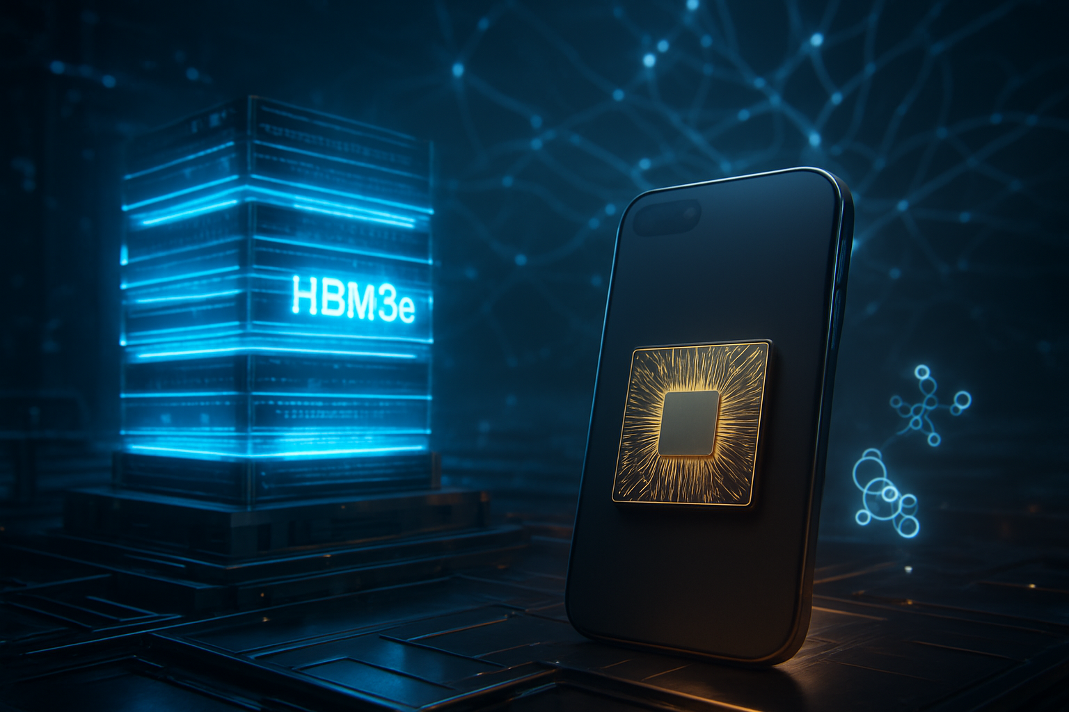
    The core of this restructuring is Samsung's aggressive push to reclaim its technological edge in the HBM market. The company has faced criticism since 2024 for lagging behind rivals like SK Hynix (KRX: 000660) in supplying HBM chips crucial for AI accelerators. The new office will spearhead efforts to accelerate the mass production of advanced HBM chips, specifically HBM4. Notably, Samsung is in "close discussion" with Nvidia (NASDAQ: NVDA), a key AI industry player, for HBM4 supply, and has secured deals to provide HBM3e chips for Broadcom (NASDAQ: AVGO) and Advanced Micro Devices (NASDAQ: AMD) new MI350 Series AI accelerators. These strategic partnerships and product developments underscore a vigorous drive to diversify its client base and solidify its position in the high-growth HBM segment, which was once considered a "biggest drag" on its financial performance.

    This organizational overhaul also coincides with the resolution of significant legal risks for Chairman Lee Jae-yong, following his acquittal by the Supreme Court in July 2025. This legal clarity has provided the impetus for the sweeping personnel changes and the establishment of the permanent Business Support Office, enabling Chairman Lee to consolidate control and prepare for future business initiatives without the shadow of prolonged legal battles. Unlike previous strategies that saw Samsung dominate in broad memory segments like DRAM and NAND flash, this new direction indicates a more targeted approach, prioritizing high-value, high-growth areas like HBM, potentially even re-evaluating its Integrated Device Manufacturer (IDM) strategy to focus more intensely on advanced memory offerings.

    Reshaping the AI Memory Landscape: Competitive Ripples and Strategic Realignment

    Samsung Electronics' reinvigorated strategic focus on High Bandwidth Memory (HBM), underpinned by its internal restructuring, is poised to send significant competitive ripples across the AI memory landscape, affecting tech giants, AI companies, and even startups. Having lagged behind in the HBM race, particularly in securing certifications for its HBM3E products, Samsung's aggressive push to reclaim its leadership position will undoubtedly intensify the battle for market share and innovation.

    The most immediate impact will be felt by its direct competitors in the HBM market. SK Hynix (KRX: 000660), which currently holds a dominant market share (estimated 55-62% as of Q2 2025), faces a formidable challenge in defending its lead. Samsung's plans to aggressively increase HBM chip production, accelerate HBM4 development with samples already shipping to key clients like Nvidia, and potentially engage in price competition, could erode SK Hynix's market share and its near-monopoly in HBM3E supply to Nvidia. Similarly, Micron Technology (NASDAQ: MU), which has recently climbed to the second spot with 20-25% market share by Q2 2025, will encounter tougher competition from Samsung in the HBM4 segment, even as it solidifies its role as a critical third supplier.

    Conversely, major consumers of HBM, such as AI chip designers Nvidia and Advanced Micro Devices (NASDAQ: AMD), stand to be significant beneficiaries. A more competitive HBM market promises greater supply stability, potentially lower costs, and accelerated technological advancements. Nvidia, already collaborating with Samsung on HBM4 development and its AI factory, will gain from a diversified HBM supply chain, reducing its reliance on a single vendor. This dynamic could also empower AI model developers and cloud AI providers, who will benefit from the increased availability of high-performance HBM, enabling the creation of more complex and efficient AI models and applications across various sectors.

    The intensified competition is also expected to shift pricing power from HBM manufacturers to their major customers, potentially leading to a 6-10% drop in HBM Average Selling Prices (ASPs) in the coming year, according to industry observers. This could disrupt existing revenue models for memory manufacturers but simultaneously fuel the "AI Supercycle" by making high-performance memory more accessible. Furthermore, Samsung's foray into AI-powered semiconductor manufacturing, utilizing over 50,000 Nvidia GPUs, signals a broader industry trend towards integrating AI into the entire chip production process, from design to quality assurance. This vertical integration strategy could present challenges for smaller AI hardware startups that lack the capital and technological expertise to compete at such a scale, while niche semiconductor design startups might find opportunities in specialized IP blocks or custom accelerators that can integrate with Samsung's advanced manufacturing processes.

    The AI Supercycle and Samsung's Resurgence: Broader Implications and Looming Challenges

    Samsung Electronics' strategic overhaul and intensified focus on High Bandwidth Memory (HBM) resonate deeply within the broader AI landscape, signaling a critical juncture in the ongoing "AI supercycle." HBM has emerged as the indispensable backbone for high-performance computing, providing the unprecedented speed, efficiency, and lower power consumption essential for advanced AI workloads, particularly in training and inferencing large language models (LLMs). Samsung's renewed commitment to HBM, driven by its restructured Business Support Office, is not merely a corporate maneuver but a strategic imperative to secure its position in an era where memory bandwidth dictates the pace of AI innovation.

    This pivot underscores HBM's transformative role in dismantling the "memory wall" that once constrained AI accelerators. The continuous push for higher bandwidth, capacity, and power efficiency across HBM generations—from HBM1 to the impending HBM4 and beyond—is fundamentally reshaping how AI systems are designed and optimized. HBM4, for instance, is projected to deliver a 200% bandwidth increase over HBM3E and up to 36 GB capacity, sufficient for high-precision LLMs, while simultaneously achieving approximately 40% lower power per bit. This level of innovation is comparable to historical breakthroughs like the transition from CPUs to GPUs for parallel processing, enabling AI to scale to unprecedented levels and accelerate discovery in deep learning.

    However, this aggressive pursuit of HBM leadership also brings potential concerns. The HBM market is effectively an oligopoly, dominated by SK Hynix (KRX: 000660), Samsung, and Micron Technology (NASDAQ: MU). SK Hynix initially gained a significant competitive edge through early investment and strong partnerships with AI chip leader Nvidia (NASDAQ: NVDA), while Samsung initially underestimated HBM's potential, viewing it as a niche market. Samsung's current push with HBM4, including reassigning personnel from its foundry unit to HBM and substantial capital expenditure, reflects a determined effort to regain lost ground. This intense competition among a few dominant players could lead to market consolidation, where only those with massive R&D budgets and manufacturing capabilities can meet the stringent demands of AI leaders.

    Furthermore, the high-stakes environment in HBM innovation creates fertile ground for intellectual property disputes. As the technology becomes more complex, involving advanced 3D stacking techniques and customized base dies, the likelihood of patent infringement claims and defensive patenting strategies increases. Such "patent wars" could slow down innovation or escalate costs across the entire AI ecosystem. The complexity and high cost of HBM production also pose challenges, contributing to the expensive nature of HBM-equipped GPUs and accelerators, thus limiting their widespread adoption primarily to enterprise and research institutions. While HBM is energy-efficient per bit, the sheer scale of AI workloads results in substantial absolute power consumption in data centers, necessitating costly cooling solutions and adding to the environmental footprint, which are critical considerations for the sustainable growth of AI.

    The Road Ahead: HBM's Evolution and the Future of AI Memory

    The trajectory of High Bandwidth Memory (HBM) is one of relentless innovation, driven by the insatiable demands of artificial intelligence and high-performance computing. Samsung Electronics' strategic repositioning underscores a commitment to not only catch up but to lead in the next generations of HBM, shaping the future of AI memory. The near-term and long-term developments in HBM technology promise to push the boundaries of bandwidth, capacity, and power efficiency, unlocking new frontiers for AI applications.

    In the near term, the focus remains squarely on HBM4, with Samsung aggressively pursuing its development and mass production for a late 2025/2026 market entry. HBM4 is projected to deliver unprecedented bandwidth, ranging from 1.2 TB/s to 2.8 TB/s per stack, and capacities up to 36GB per stack through 12-high configurations, potentially reaching 64GB. A critical innovation in HBM4 is the introduction of client-specific 'base die' layers, allowing processor vendors like Nvidia (NASDAQ: NVDA) and Advanced Micro Devices (NASDAQ: AMD) to design custom base dies that integrate portions of GPU functionality directly into the HBM stack. This customization capability, coupled with Samsung's transition to FinFET-based logic processes for HBM4, promises significant performance boosts, area reduction, and power efficiency improvements, targeting a 50% power reduction with its new process.

    Looking further ahead, HBM5, anticipated around 2028-2029, is projected to achieve bandwidths of 4 TB/s per stack and capacities scaling up to 80GB using 16-high stacks, with some roadmaps even hinting at 20-24 layers by 2030. Advanced bonding technologies like wafer-to-wafer (W2W) hybrid bonding are expected to become mainstream from HBM5, crucial for higher I/O counts, lower power consumption, and improved heat dissipation. Moreover, future HBM generations may incorporate Processing-in-Memory (PIM) or Near-Memory Computing (NMC) structures, further reducing data movement and enhancing bandwidth by bringing computation closer to the data.

    These technological advancements will fuel a proliferation of new AI applications and use cases. HBM's high bandwidth and low power consumption make it a game-changer for edge AI and machine learning, enabling more efficient processing in resource-constrained environments for real-time analytics in smart cities, industrial IoT, autonomous vehicles, and portable healthcare. For specialized generative AI, HBM is indispensable for accelerating the training and inference of complex models with billions of parameters, enabling faster response times for applications like chatbots and image generation. The synergy between HBM and other technologies like Compute Express Link (CXL) will further enhance memory expansion, pooling, and sharing across heterogeneous computing environments, accelerating AI development across the board.

    However, significant challenges persist. Power consumption remains a critical concern; while HBM is energy-efficient per bit, the overall power consumption of HBM-powered AI systems continues to rise, necessitating advanced thermal management solutions like immersion cooling for future generations. Manufacturing complexity, particularly with 3D-stacked architectures and the transition to advanced packaging, poses yield challenges and increases production costs. Supply chain resilience is another major hurdle, given the highly concentrated HBM market dominated by just three major players. Experts predict an intensified competitive landscape, with the "real showdown" in the HBM market commencing with HBM4. Samsung's aggressive pricing strategies and accelerated development, coupled with Nvidia's pivotal role in influencing HBM roadmaps, will shape the future market dynamics. The HBM market is projected for explosive growth, with its revenue share within the DRAM market expected to reach 50% by 2030, making technological leadership in HBM a critical determinant of success for memory manufacturers in the AI era.

    A New Era for Samsung and the AI Memory Market

    Samsung Electronics' strategic transition of its business support office, coinciding with a renewed and aggressive focus on High Bandwidth Memory (HBM), marks a pivotal moment in the company's history and for the broader AI memory chip sector. After navigating a period of legal challenges and facing criticism for falling behind in the HBM race, Samsung is clearly signaling its intent to reclaim its leadership position through a comprehensive organizational overhaul and substantial investments in next-generation memory technology.

    The key takeaways from this development are Samsung's determined ambition to not only catch up but to lead in the HBM4 era, its critical reliance on strong partnerships with AI industry giants like Nvidia (NASDAQ: NVDA), and the strategic shift towards a more customer-centric and customizable "Open HBM" approach. The significant capital expenditure and the establishment of an AI-powered manufacturing facility underscore the lucrative nature of the AI memory market and Samsung's commitment to integrating AI into every facet of its operations.

    In the grand narrative of AI history, HBM chips are not merely components but foundational enablers. They have fundamentally addressed the "memory wall" bottleneck, allowing GPUs and AI accelerators to process the immense data volumes required by modern large language models and complex generative AI applications. Samsung's pioneering efforts in concepts like Processing-in-Memory (PIM) further highlight memory's evolving role from a passive storage unit to an active computational element, a crucial step towards more energy-efficient and powerful AI systems. This strategic pivot is an assessment of memory's significance in AI history as a continuous trajectory of innovation, where advancements in hardware directly unlock new algorithmic and application possibilities.

    The long-term impact of Samsung's HBM strategy will be a sustained acceleration of AI growth, fueled by a robust and competitive HBM supply chain. This renewed competition among the few dominant players—Samsung, SK Hynix (KRX: 000660), and Micron Technology (NASDAQ: MU)—will drive continuous innovation, pushing the boundaries of bandwidth, capacity, and energy efficiency. Samsung's vertical integration advantage, spanning memory and foundry operations, positions it uniquely to control costs and timelines in the complex HBM production process, potentially reshaping market leadership dynamics in the coming years. The "Open HBM" strategy could also foster a more collaborative ecosystem, leading to highly specialized and optimized AI hardware solutions.

    In the coming weeks and months, the industry will be closely watching the qualification results of Samsung's HBM4 samples with key customers like Nvidia. Successful certification will be a major validation of Samsung's technological prowess and a crucial step towards securing significant orders. Progress in achieving high yield rates for HBM4 mass production, along with competitive responses from SK Hynix and Micron regarding their own HBM4 roadmaps and customer engagements, will further define the evolving landscape of the "HBM Wars." Any additional collaborations between Samsung and Nvidia, as well as developments in complementary technologies like CXL and PIM, will also provide important insights into Samsung's broader AI memory strategy and its potential to regain the "memory crown" in this critical AI era.


    This content is intended for informational purposes only and represents analysis of current AI developments.

    TokenRing AI delivers enterprise-grade solutions for multi-agent AI workflow orchestration, AI-powered development tools, and seamless remote collaboration platforms.
    For more information, visit https://www.tokenring.ai/.

  • Micron Technology: Powering the AI Revolution and Reshaping the Semiconductor Landscape

    Micron Technology: Powering the AI Revolution and Reshaping the Semiconductor Landscape

    Micron Technology (NASDAQ: MU) has emerged as an undeniable powerhouse in the semiconductor industry, propelled by the insatiable global demand for high-bandwidth memory (HBM) – the critical fuel for the burgeoning artificial intelligence (AI) revolution. The company's recent stellar stock performance and escalating market capitalization underscore a profound re-evaluation of memory's role, transforming it from a cyclical commodity to a strategic imperative in the AI era. As of November 2025, Micron's market cap hovers around $245 billion, cementing its position as a key market mover and a bellwether for the future of AI infrastructure.

    This remarkable ascent is not merely a market anomaly but a direct reflection of Micron's strategic foresight and technological prowess in delivering the high-performance, energy-efficient memory solutions that underpin modern AI. With its HBM3e chips now powering the most advanced AI accelerators from industry giants, Micron is not just participating in the AI supercycle; it is actively enabling the computational leaps that define it, driving unprecedented growth and reshaping the competitive landscape of the global tech industry.

    The Technical Backbone of AI: Micron's Memory Innovations

    Micron Technology's deep technical expertise in memory solutions, spanning DRAM, High Bandwidth Memory (HBM), and NAND, forms the essential backbone for today's most demanding AI and high-performance computing (HPC) workloads. These technologies are meticulously engineered for unprecedented bandwidth, low latency, expansive capacity, and superior power efficiency, setting them apart from previous generations and competitive offerings.

    At the forefront is Micron's HBM, a critical component for AI training and inference. Its HBM3E, for instance, delivers industry-leading performance with bandwidth exceeding 1.2 TB/s and pin speeds greater than 9.2 Gbps. Available in 8-high stacks with 24GB capacity and 12-high stacks with 36GB capacity, the 8-high cube offers 50% more memory capacity per stack. Crucially, Micron's HBM3E boasts 30% lower power consumption than competitors, a vital differentiator for managing the immense energy and thermal challenges of AI data centers. This efficiency is achieved through advanced CMOS innovations, Micron's 1β process technology, and advanced packaging techniques. The company is also actively sampling HBM4, promising even greater bandwidth (over 2.0 TB/s per stack) and a 20% improvement in power efficiency, with plans for a customizable base die for enhanced caches and specialized AI/HPC interfaces.

    Beyond HBM, Micron's LPDDR5X, built on the world's first 1γ (1-gamma) process node, achieves data rates up to 10.7 Gbps with up to 20% power savings. This low-power, high-speed DRAM is indispensable for AI at the edge, accelerating on-device AI applications in mobile phones and autonomous vehicles. The use of Extreme Ultraviolet (EUV) lithography in the 1γ node enables denser bitline and wordline spacing, crucial for high-speed I/O within strict power budgets. For data centers, Micron's DDR5 MRDIMMs offer up to a 39% increase in effective memory bandwidth and 40% lower latency, while CXL (Compute Express Link) memory expansion modules provide a flexible way to pool and disaggregate memory, boosting read-only bandwidth by 24% and mixed read/write bandwidth by up to 39% across HPC and AI workloads.

    In the realm of storage, Micron's advanced NAND flash, particularly its 232-layer 3D NAND (G8 NAND) and 9th Generation (G9) TLC NAND, provides the foundational capacity for the colossal datasets that AI models consume. The G8 NAND offers over 45% higher bit density and the industry's fastest NAND I/O speed of 2.4 GB/s, while the G9 TLC NAND boasts an industry-leading transfer speed of 3.6 GB/s and is integrated into Micron's PCIe Gen6 NVMe SSDs, delivering up to 28 GB/s sequential read speeds. These advancements are critical for data ingestion, persistent storage, and rapid data access in AI training and retrieval-augmented generation (RAG) pipelines, ensuring seamless data flow throughout the AI lifecycle.

    Reshaping the AI Ecosystem: Beneficiaries and Competitive Dynamics

    Micron Technology's advanced memory solutions are not just components; they are enablers, profoundly impacting the strategic positioning and competitive dynamics of AI companies, tech giants, and innovative startups across the globe. The demand for Micron's high-performance memory is directly fueling the ambitions of the most prominent players in the AI race.

    Foremost among the beneficiaries are leading AI chip developers and hyperscale cloud providers. NVIDIA (NASDAQ: NVDA), a dominant force in AI accelerators, relies heavily on Micron's HBM3E chips for its next-generation Blackwell Ultra, H100, H800, and H200 Tensor Core GPUs. This symbiotic relationship is crucial for NVIDIA's projected $150 billion in AI chip sales in 2025. Similarly, AMD (NASDAQ: AMD) is integrating Micron's HBM3E into its upcoming Instinct MI350 Series GPUs, targeting large AI model training and HPC. Hyperscale cloud providers like Microsoft (NASDAQ: MSFT), Google (NASDAQ: GOOGL), and Amazon (NASDAQ: AMZN) are significant consumers of Micron's memory and storage, utilizing them to scale their AI capabilities, manage distributed AI architectures, and optimize energy consumption in their vast data centers, even as they develop their own custom AI chips. Major AI labs, including OpenAI, also require "tons of compute, tons of memory" for their cutting-edge AI infrastructure, making them key customers.

    The competitive landscape within the memory sector has intensified dramatically, with Micron positioned as a leading contender in the high-stakes HBM market, alongside SK Hynix (KRX: 000660) and Samsung (KRX: 005930). Micron's HBM3E's 30% lower power consumption offers a significant competitive advantage, translating into substantial operational cost savings and more sustainable AI data centers for its customers. As the only major U.S.-based memory manufacturer, Micron also enjoys a unique strategic advantage in terms of supply chain resilience and geopolitical considerations. However, the aggressive ramp-up in HBM production by competitors could lead to a potential oversupply by 2027, potentially impacting pricing. Furthermore, reported delays in Micron's HBM4 could temporarily cede an advantage to its rivals in the next generation of HBM.

    The impact extends beyond the data center. Smartphone manufacturers leverage Micron's LPDDR5X for on-device AI, enabling faster experiences and longer battery life for AI-powered features. The automotive industry utilizes LPDDR5X and GDDR6 for advanced driver-assistance systems (ADAS), while the gaming sector benefits from GDDR6X and GDDR7 for immersive, AI-enhanced gameplay. Micron's strategic reorganization into customer-focused business units—Cloud Memory Business Unit (CMBU), Core Data Center Business Unit (CDBU), Mobile and Client Business Unit (MCBU), and Automotive and Embedded Business Unit (AEBU)—further solidifies its market positioning, ensuring tailored solutions for each segment of the AI ecosystem. With its entire 2025 HBM production capacity sold out and bookings extending into 2026, Micron has secured robust demand, driving significant revenue growth and expanding profit margins.

    Wider Significance: Micron's Role in the AI Landscape

    Micron Technology's pivotal role in the AI landscape transcends mere component supply; it represents a fundamental re-architecture of how AI systems are built and operated. The company's continuous innovations in memory and storage are not just keeping pace with AI's demands but are actively shaping its trajectory, addressing critical bottlenecks and enabling capabilities previously thought impossible.

    This era marks a profound shift where memory has transitioned from a commoditized product to a strategic asset. In previous technology cycles, memory was often a secondary consideration, but the AI revolution has elevated advanced memory, particularly HBM, to a critical determinant of AI performance and innovation. We are witnessing an "AI supercycle," a period of structural and persistent demand for specialized memory infrastructure, distinct from prior boom-and-bust patterns. Micron's advancements in HBM, LPDDR, GDDR, and advanced NAND are directly enabling faster training and inference for AI models, supporting larger models and datasets with billions of parameters, and enhancing multi-GPU and distributed computing architectures. The focus on energy efficiency in technologies like HBM3E and 1-gamma DRAM is also crucial for mitigating the substantial energy demands of AI data centers, contributing to more sustainable and cost-effective AI operations.

    Moreover, Micron's solutions are vital for the burgeoning field of edge AI, facilitating real-time processing and decision-making on devices like autonomous vehicles and smartphones, thereby reducing reliance on cloud infrastructure and enhancing privacy. This expansion of AI from centralized cloud data centers to the intelligent edge is a key trend, and Micron is a crucial enabler of this distributed AI model.

    Despite its strong position, Micron faces inherent challenges. Intense competition from rivals like SK Hynix and Samsung in the HBM market could lead to pricing pressures. The "memory wall" remains a persistent bottleneck, where the speed of processing often outpaces memory delivery, limiting AI performance. Balancing performance with power efficiency is an ongoing challenge, as is the complexity and risk associated with developing entirely new memory technologies. Furthermore, the rapid evolution of AI makes it difficult to predict future needs, and geopolitical factors, such as regulations mandating domestic AI chips, could impact market access. Nevertheless, Micron's commitment to technological leadership and its strategic investments position it as a foundational player in overcoming these challenges and continuing to drive AI advancement.

    The Horizon: Future Developments and Expert Predictions

    Looking ahead, Micron Technology is poised for continued significant developments in the AI and semiconductor landscape, with a clear roadmap for advancing HBM, CXL, and process node technologies. These innovations are critical for sustaining the momentum of the AI supercycle and addressing the ever-growing demands of future AI workloads.

    In the near term (late 2024 – 2026), Micron is aggressively scaling its HBM3E production, with its 24GB 8-High solution already integrated into NVIDIA (NASDAQ: NVDA) H200 Tensor Core GPUs. The company is also sampling its 36GB 12-High HBM3E, promising superior performance and energy efficiency. Micron aims to significantly increase its HBM market share to 20-25% by 2026, supported by capacity expansion, including a new HBM packaging facility in Singapore by 2026. Simultaneously, Micron's CZ120 CXL memory expansion modules are in sample availability, designed to provide flexible memory scaling for various workloads. In DRAM, the 1-gamma (1γ) node, utilizing EUV lithography, is being sampled, offering speed increases and lower power consumption. For NAND, volume production of 232-layer 3D NAND (G8) and G9 TLC NAND continues to drive performance and density.

    Longer term (2027 and beyond), Micron's HBM roadmap includes HBM4, projected for mass production in 2025, offering a 40% increase in bandwidth and 70% reduction in power consumption compared to HBM3E. HBM4E is anticipated by 2028, targeting 48GB to 64GB stack capacities and over 2 TB/s bandwidth, followed by HBM5 (2029) and HBM6 (2032) with even more ambitious bandwidth targets. CXL 3.0/3.1 will be crucial for memory pooling and disaggregation, enabling dynamic memory access for CPUs and GPUs in complex AI/HPC workloads. Micron's DRAM roadmap extends to the 1-delta (1δ) node, potentially skipping the 8th-generation 10nm process for a direct leap to a 9nm DRAM node. In NAND, the company envisions 500+ layer 3D NAND for even greater storage density.

    These advancements will unlock a wide array of potential applications: HBM for next-generation LLM training and AI accelerators, CXL for optimizing data center performance and TCO, and low-power DRAM for enabling sophisticated AI on edge devices like AI PCs, smartphones, AR/VR headsets, and autonomous vehicles. However, challenges persist, including intensifying competition, technological hurdles (e.g., reported HBM4 yield challenges), and the need for scalable and resilient supply chains. Experts remain overwhelmingly bullish, predicting Micron's fiscal 2025 earnings to surge by nearly 1000%, driven by the AI-driven supercycle. The HBM market is projected to expand from $4 billion in 2023 to over $25 billion by 2025, potentially exceeding $100 billion by 2030, directly fueling Micron's sustained growth and profitability.

    A New Era: Micron's Enduring Impact on AI

    Micron Technology's journey as a key market cap stock mover is intrinsically linked to its foundational role in powering the artificial intelligence revolution. The company's strategic investments, relentless innovation, and leadership in high-bandwidth, low-power, and high-capacity memory solutions have firmly established it as an indispensable enabler of modern AI.

    The key takeaway is clear: advanced memory is no longer a peripheral component but a central strategic asset in the AI era. Micron's HBM solutions, in particular, are facilitating the "computational leaps" required for cutting-edge AI acceleration, from training massive language models to enabling real-time inference at the edge. This period of intense AI-driven demand and technological innovation is fundamentally re-architecting the global technology landscape, with Micron at its epicenter.

    The long-term impact of Micron's contributions is expected to be profound and enduring. The AI supercycle promises a new paradigm of more stable pricing and higher margins for leading memory manufacturers, positioning Micron for sustained growth well into the next decade. Its strategic focus on HBM and next-generation technologies like HBM4, coupled with investments in energy-efficient solutions and advanced packaging, are crucial for maintaining its leadership and supporting the ever-increasing computational demands of AI while prioritizing sustainability.

    In the coming weeks and months, industry observers and investors should closely watch Micron's upcoming fiscal first-quarter results, anticipated around December 17, for further insights into its performance and outlook. Continued strong demand for AI-fueled memory into 2026 will be a critical indicator of the supercycle's longevity. Progress in HBM4 development and adoption, alongside the competitive landscape dominated by Samsung (KRX: 005930) and SK Hynix (KRX: 000660), will shape market dynamics. Additionally, overall pricing trends for standard DRAM and NAND will provide a broader view of the memory market's health. While the fundamentals are strong, the rapid climb in Micron's stock suggests potential for short-term volatility, and careful assessment of growth potential versus current valuation will be essential. Micron is not just riding the AI wave; it is helping to generate its immense power.


    This content is intended for informational purposes only and represents analysis of current AI developments.

    TokenRing AI delivers enterprise-grade solutions for multi-agent AI workflow orchestration, AI-powered development tools, and seamless remote collaboration platforms.
    For more information, visit https://www.tokenring.ai/.