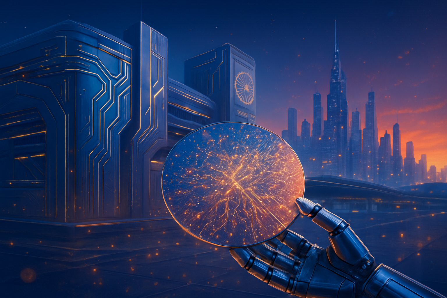
For decades, the "Memory Wall"—the widening performance gap between lightning-fast processors and significantly slower memory—has been the single greatest hurdle to achieving peak artificial intelligence efficiency. As of early 2026, the semiconductor industry is no longer just chipping away at this wall; it is tearing it down. The shift from planar, two-dimensional memory to vertical 3D DRAM and the integration of Processing-In-Memory (PIM) has officially moved from the laboratory to the production floor, promising to fundamentally rewrite the energy physics of modern computing.
This architectural revolution is arriving just in time. As next-generation large language models (LLMs) and multi-modal agents demand trillions of parameters and near-instantaneous response times, traditional hardware configurations have hit a "Power Wall." By eliminating the energy-intensive movement of data across the motherboard, these new memory architectures are enabling AI capabilities that were computationally impossible just two years ago. The industry is witnessing a transition where memory is no longer a passive storage bin, but an active participant in the thinking process.
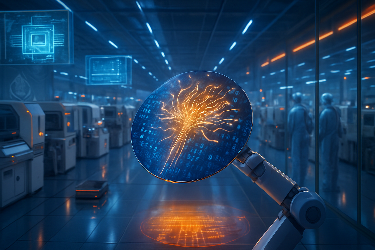
The Technical Leap: Vertical Stacking and Computing at Rest
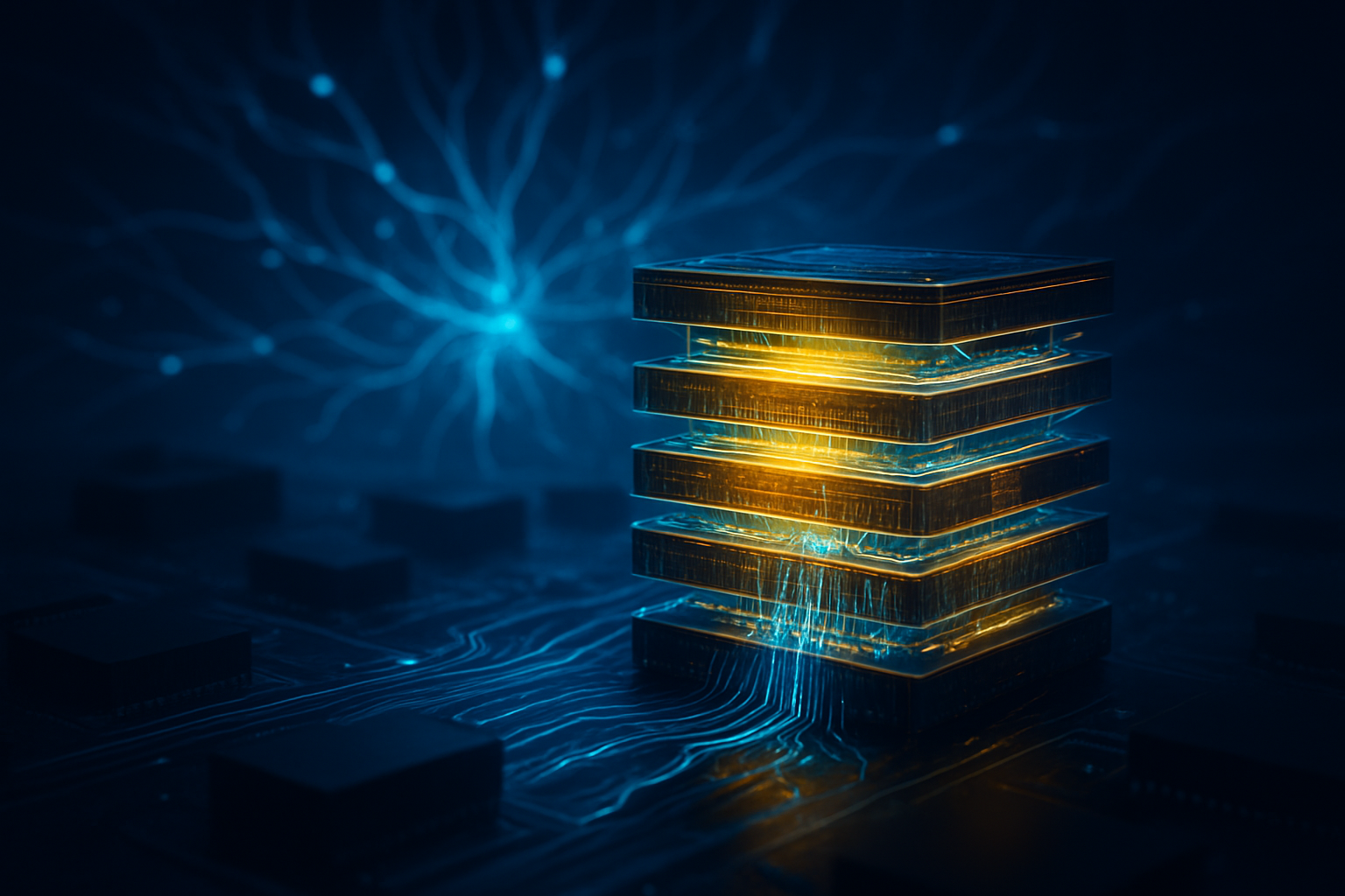
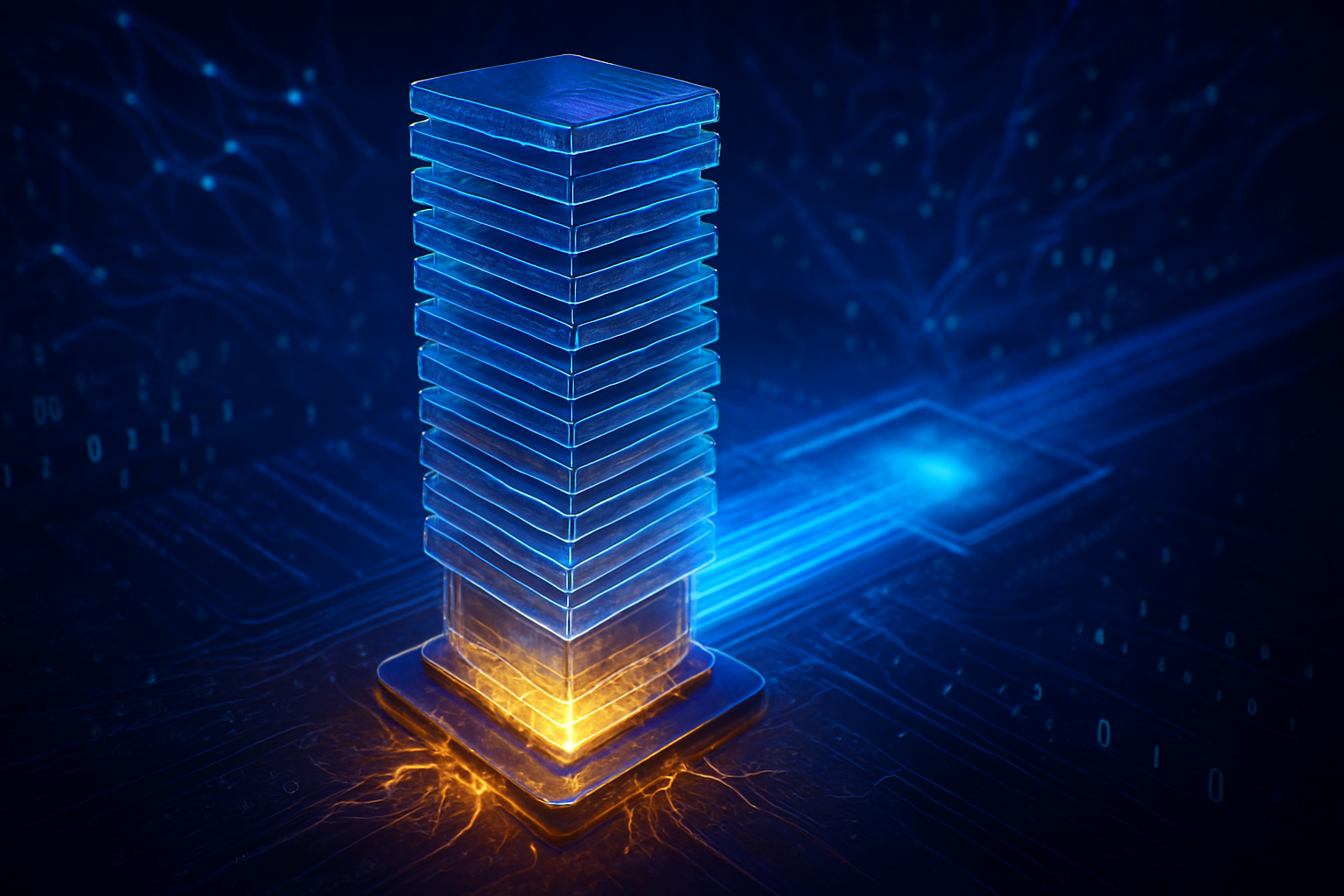
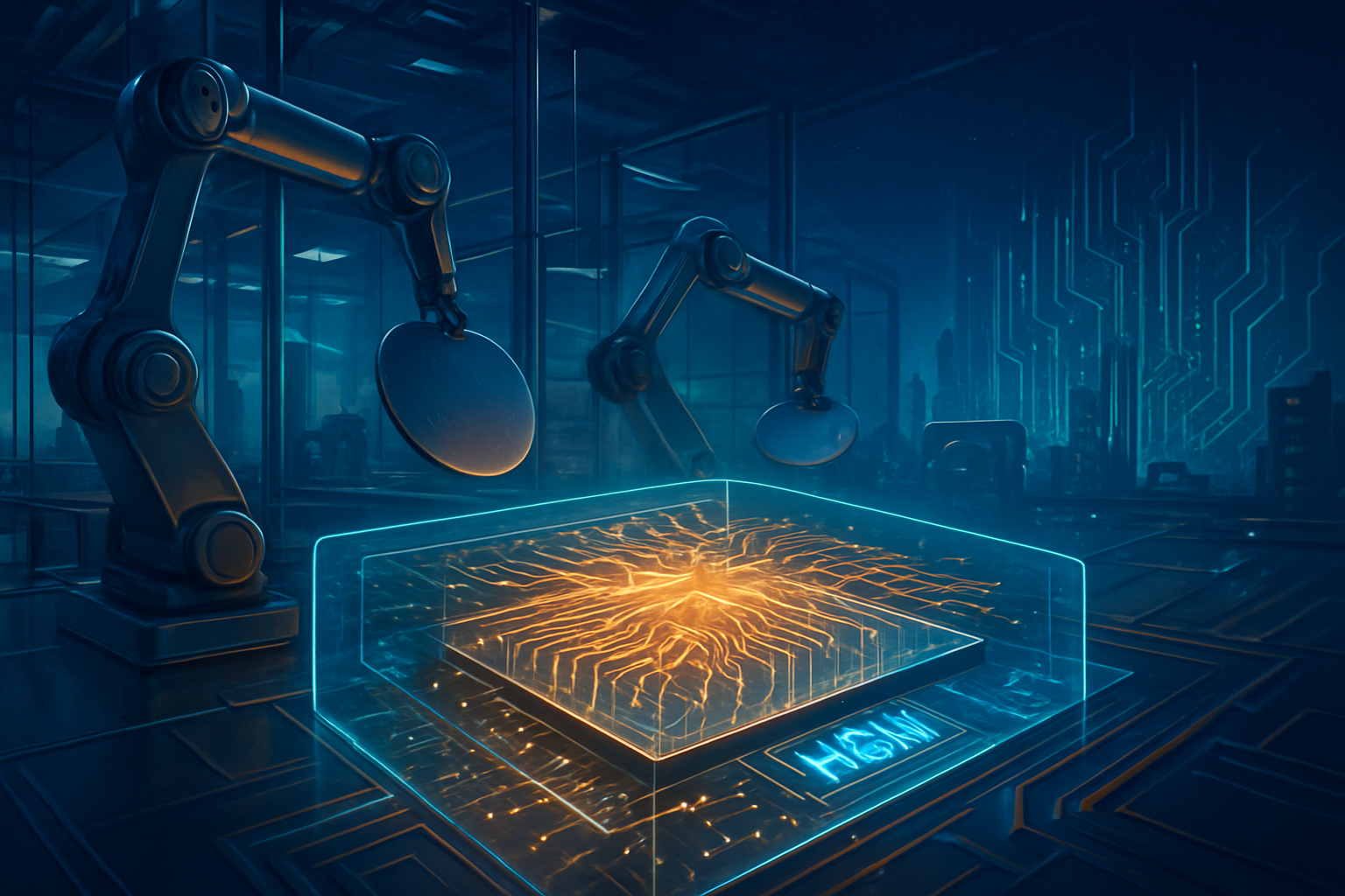
The most significant shift in memory fabrication is the transition to Vertical Channel Transistor (VCT) technology. Samsung (KRX:005930) has pioneered this move with the introduction of 4F² (four-square-feature) DRAM cell structures, which stack transistors vertically to reduce the physical footprint of each cell. By early 2026, this has allowed manufacturers to shrink die areas by 30% while increasing performance by 50%. Simultaneously, SK Hynix (KRX:000660) has pushed the boundaries of High Bandwidth Memory with its 16-Hi HBM4 modules. These units utilize "Hybrid Bonding" to connect memory dies directly without traditional micro-bumps, resulting in a thinner profile and dramatically better thermal conductivity—a critical factor for AI chips that generate intense heat.
Processing-In-Memory (PIM) takes this a step further by integrating AI engines directly into the memory banks themselves. This architecture addresses the "Von Neumann bottleneck," where the constant shuffling of data between the memory and the processor (GPU or CPU) consumes up to 1,000 times more energy than the actual calculation. In early 2026, the finalization of the LPDDR6-PIM standard has brought this technology to mobile devices, allowing for local "Multiply-Accumulate" (MAC) operations. This means that a smartphone or edge device can now run complex LLM inference locally with a 21% increase in energy efficiency and double the performance of previous generations.
Initial reactions from the AI research community have been overwhelmingly positive. Dr. Elena Rodriguez, a senior fellow at the AI Hardware Institute, noted that "we have spent ten years optimizing software to hide memory latency; with 3D DRAM and PIM, that latency is finally beginning to disappear at the hardware level." This shift allows researchers to design models with even larger context windows and higher reasoning capabilities without the crippling power costs that previously stalled deployment.
The Competitive Landscape: The "Big Three" and the Foundry Alliance
The race to dominate this new memory era has created a fierce rivalry between Samsung, SK Hynix, and Micron (NASDAQ:MU). While Samsung has focused on the 4F² vertical transition for mass-market DRAM, Micron has taken a more aggressive "Direct to 3D" approach, skipping transitional phases to focus on HBM4 with a 2048-bit interface. This move has paid off; Micron has reportedly locked in its entire 2026 production capacity for HBM4 with major AI accelerator clients. The strategic advantage here is clear: companies that control the fastest, most efficient memory will dictate the performance ceiling for the next generation of AI GPUs.
The development of Custom HBM (cHBM) has also forced a deeper collaboration between memory makers and foundries like TSMC (NYSE:TSM). In 2026, we are seeing "Logic-in-Base-Die" designs where SK Hynix and TSMC integrate GPU-like logic directly into the foundation of a memory stack. This effectively turns the memory module into a co-processor. This trend is a direct challenge to the traditional dominance of pure-play chip designers, as memory companies begin to capture a larger share of the value chain.
For tech giants like NVIDIA (NASDAQ:NVDA), these innovations are essential to maintaining the momentum of their AI data center business. By integrating PIM and 16-layer HBM4 into their 2026 Blackwell-successors, they can offer massive performance-per-watt gains that satisfy the tightening environmental and energy regulations faced by data center operators. Startups specializing in "Edge AI" also stand to benefit, as PIM-enabled LPDDR6 allows them to deploy sophisticated agents on hardware that previously lacked the thermal and battery headroom.
Wider Significance: Breaking the Energy Deadlock
The broader significance of 3D DRAM and PIM lies in its potential to solve the AI energy crisis. As of 2026, global power consumption from data centers has become a primary concern for policymakers. Because moving data "over the bus" is the most energy-intensive part of AI workloads, processing data "at rest" within the memory cells represents a paradigm shift. Experts estimate that PIM architectures can reduce power consumption for specific AI workloads by up to 80%, a milestone that makes the dream of sustainable, ubiquitous AI more realistic.
This development mirrors previous milestones like the transition from HDDs to SSDs, but with much higher stakes. While SSDs changed storage speed, 3D DRAM and PIM are changing the nature of computation itself. There are, however, concerns regarding the complexity of manufacturing and the potential for lower yields as vertical stacking pushes the limits of material science. Some industry analysts worry that the high cost of HBM4 and 3D DRAM could widen the "AI divide," where only the wealthiest tech companies can afford the most efficient hardware, leaving smaller players to struggle with legacy, energy-hungry systems.
Furthermore, these advancements represent a structural shift toward "near-data processing." This trend is expected to move the focus of AI optimization away from just making "bigger" models and toward making models that are smarter about how they access and store information. It aligns with the growing industry trend of sovereign AI and localized data processing, where privacy and speed are paramount.
Future Horizons: From HBM4 to Truly Autonomous Silicon
Looking ahead, the near-term future will likely see the expansion of PIM into every facet of consumer electronics. Within the next 24 months, we expect to see the first "AI-native" PCs and automobiles that utilize 3D DRAM to handle real-time sensor fusion and local reasoning without a constant connection to the cloud. The long-term vision involves "Cognitive Memory," where the distinction between the processor and the memory becomes entirely blurred, creating a unified fabric of silicon that can learn and adapt in real-time.
However, significant challenges remain. Standardizing the software stack so that developers can easily write code for PIM-enabled chips is a major undertaking. Currently, many AI frameworks are still optimized for traditional GPU architectures, and a "re-tooling" of the software ecosystem is required to fully exploit the 80% energy savings promised by PIM. Experts predict that the next two years will be defined by a "Software-Hardware Co-design" movement, where AI models are built specifically to live within the architecture of 3D memory.
A New Foundation for Intelligence
The arrival of 3D DRAM and Processing-In-Memory marks the end of the traditional computer architecture that has dominated the industry since the mid-20th century. By moving computation into the memory and stacking cells vertically, the industry has found a way to bypass the physical constraints that threatened to stall the AI revolution. The 2026 breakthroughs from Samsung, SK Hynix, and Micron have effectively moved the "Memory Wall" far enough into the distance to allow for a new generation of hyper-capable AI models.
As we move forward, the most important metric for AI success will likely shift from "FLOPs" (floating-point operations per second) to "Efficiency-per-Bit." This evolution in memory architecture is not just a technical upgrade; it is a fundamental reimagining of how machines think. In the coming weeks and months, all eyes will be on the first mass-market deployments of HBM4 and LPDDR6-PIM, as the industry begins to see just how far the AI revolution can go when it is no longer held back by the physics of data movement.
This content is intended for informational purposes only and represents analysis of current AI developments.
TokenRing AI delivers enterprise-grade solutions for multi-agent AI workflow orchestration, AI-powered development tools, and seamless remote collaboration platforms.
For more information, visit https://www.tokenring.ai/.