CLAY, N.Y. — Micron Technology (NASDAQ: MU) has officially broken ground on its historic $100 billion semiconductor mega-site in Central New York, marking the start of the largest private investment in the state’s history. Dubbed the "Silicon Empire," the massive project in the town of Clay is designed to secure the United States' domestic supply of DRAM (Dynamic Random Access Memory), a foundational component of the global artificial intelligence infrastructure.
The groundbreaking ceremony, held at the White Pine Commerce Park, represents a pivotal victory for the CHIPS and Science Act and the Biden-Harris administration’s long-term strategy to reshore critical technology. With a commitment to producing 40% of Micron's global DRAM supply on U.S. soil by the 2040s, this facility is intended to insulate the American AI industry from geopolitical volatility in East Asia, where memory manufacturing has been concentrated for decades.
Technical Specifications and the Push for 1-Gamma Nodes
The "Silicon Empire" is not merely a manufacturing plant; it is a sprawling technological complex that will eventually house four massive fabrication plants (fabs). At the heart of these facilities is the transition to the 1-gamma (1γ) process node. This next-generation manufacturing technology utilizes Extreme Ultraviolet (EUV) lithography to etch features smaller than 10 nanometers onto silicon wafers. By implementing EUV at scale in New York, Micron aims to achieve higher density and energy efficiency in its memory chips, which are critical requirements for the power-hungry data centers fueling modern Large Language Models (LLMs).
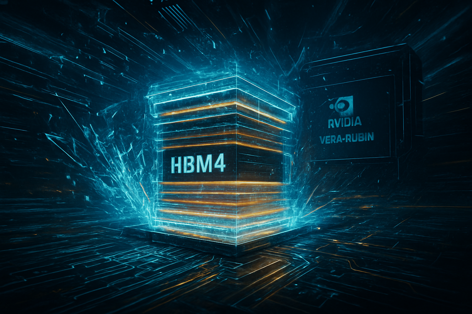
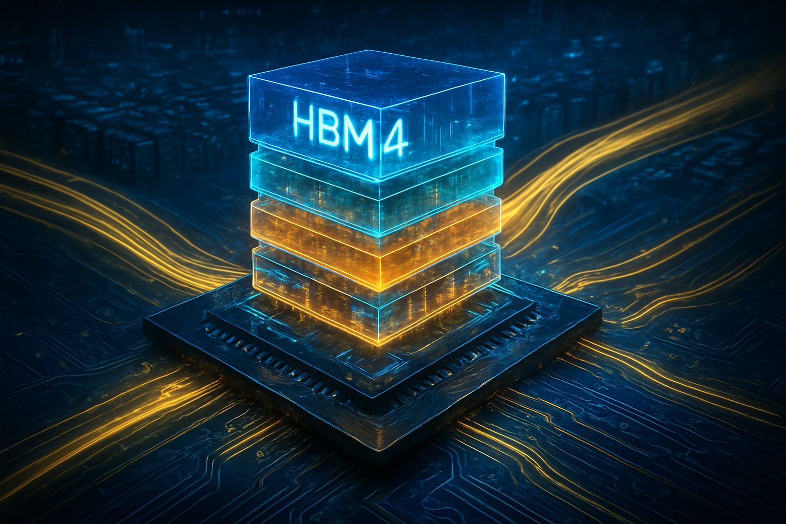
Each of the four planned cleanrooms will span approximately 600,000 square feet, totaling an unprecedented 2.4 million square feet of cleanroom space—roughly the equivalent of 40 football fields. This massive scale is necessary to address the "Memory Wall," a bottleneck in AI performance where the speed of data transfer between the processor and memory lags behind the processing power of the GPU. Micron’s New York fabs will focus on high-volume production of High Bandwidth Memory (HBM), specifically designed to sit close to AI accelerators to minimize latency.
Initial reactions from the industry have been overwhelmingly positive, though some experts note the technical hurdles ahead. Moving from pilot production in Idaho and Taiwan to high-volume manufacturing in New York using 1-gamma nodes and advanced EUV machinery is a logistical feat. However, the AI research community views the project as a necessary step toward sustaining the scaling laws of AI, which demand exponential increases in memory capacity and bandwidth every few years.
Reshaping the AI Supply Chain: Winners and Losers
The domestic production of DRAM and HBM in New York will have profound implications for AI giants and hardware manufacturers alike. Companies like NVIDIA (NASDAQ: NVDA), Advanced Micro Devices (NASDAQ: AMD), and Intel (NASDAQ: INTC) stand to benefit the most from a shortened, more reliable supply chain. By reducing the reliance on South Korean leaders like Samsung and SK Hynix, U.S. chipmakers can lower the risk of supply disruptions that have previously sent prices skyrocketing and delayed AI server deployments.
From a strategic standpoint, Micron’s expansion shifts the competitive balance of the global memory market. For years, the U.S. has dominated the design of AI logic chips but outsourced the "storage" of that data to overseas foundries. By integrating memory production into the domestic ecosystem, the "Silicon Empire" provides a logistical advantage for the hyperscalers—Amazon (NASDAQ: AMZN), Google (NASDAQ: GOOGL), and Microsoft (NASDAQ: MSFT)—who are racing to build out their own custom AI silicon and cloud infrastructure.
However, the road to dominance is not without competition. While Micron cements its footprint in New York, its South Korean rivals are also investing heavily in domestic and international expansion. The market positioning of the "Silicon Empire" hinges on its ability to produce HBM4 and future generations of memory faster and more cost-effectively than its competitors. If Micron can successfully leverage the billions in federal subsidies to undercut global pricing or offer superior integration with U.S.-made GPUs, it could significantly erode the market share of established Asian players.
National Security and the Broader AI Landscape
The significance of the Clay facility extends far beyond corporate balance sheets; it is a matter of national and economic security. In the current geopolitical climate, the concentration of semiconductor manufacturing in the Indo-Pacific region has been identified as a single point of failure for the American economy. By reshoring memory production, the U.S. is creating a "technological moat" that ensures the brains of the AI revolution remain within its borders, even in the event of regional conflict or trade embargoes.
Furthermore, the "Silicon Empire" serves as the anchor for the broader "NY SMART I-Corridor," a regional tech hub stretching from Buffalo to Syracuse. This initiative aims to revitalize the Rust Belt by creating a high-tech manufacturing ecosystem similar to Silicon Valley. The project is expected to create 9,000 direct Micron jobs and upwards of 40,000 to 50,000 indirect community jobs, including specialized roles in logistics, chemical supply, and engineering services.
Comparatively, this milestone is being viewed as the modern-day equivalent of the Erie Canal for New York—a transformative infrastructure project that redefines the state’s economic identity. While concerns have been raised regarding the environmental impact, including wastewater management and the preservation of local habitats, Micron has committed to a "Green CHIPS" framework, utilizing 100% renewable energy and achieving industry-leading water recycling rates.
The Horizon: From Groundbreaking to 2030 and Beyond
While the groundbreaking is a monumental step, the "Silicon Empire" is a long-term play. The first fab is not expected to reach operational status until 2030, with the full four-fab campus not reaching maturity until 2045. In the near term, the focus will shift to site preparation and the construction of massive infrastructure to support the facility's power and water needs. We can expect to see a flurry of secondary investments in the Syracuse area as suppliers for gases, chemicals, and equipment move into the region to support Micron’s operations.
The next critical phase for Micron will be the installation of the first EUV lithography machines, which are among the most complex pieces of equipment ever created. Experts will be watching closely to see how Micron manages the transition of its 1-gamma process node from development labs to high-volume manufacturing in a brand-new facility. Challenges such as labor shortages in the construction and engineering sectors could still pose risks to the timeline, though the massive influx of state and federal support is designed to mitigate these pressures.
A New Era for American Silicon
The groundbreaking in Clay, New York, signifies the dawn of a new era for American semiconductor manufacturing. Micron’s $100 billion "Silicon Empire" is a testament to the power of industrial policy and the recognition that memory is a strategic asset in the age of artificial intelligence. By successfully reshoring 40% of its DRAM production, Micron is not just building a factory; it is building a foundation for the next century of American innovation.
As the first walls of the mega-fab rise over the coming years, the project will serve as a bellwether for the success of the CHIPS Act. If the "Silicon Empire" can deliver on its promises of technological leadership and economic revitalization, it will provide a blueprint for other critical industries to return to U.S. shores. For now, all eyes are on Central New York as it begins its journey toward becoming the beating heart of the global AI supply chain.
This content is intended for informational purposes only and represents analysis of current AI developments.
TokenRing AI delivers enterprise-grade solutions for multi-agent AI workflow orchestration, AI-powered development tools, and seamless remote collaboration platforms.
For more information, visit https://www.tokenring.ai/.