Tag: Micron

  • The AI Memory Supercycle: Micron Shatters Records as HBM Capacity Sells Out Through 2026

    The AI Memory Supercycle: Micron Shatters Records as HBM Capacity Sells Out Through 2026

    In a definitive signal that the artificial intelligence infrastructure boom is far from over, Micron Technology (NASDAQ: MU) has delivered a fiscal first-quarter 2026 earnings report that has sent shockwaves through the semiconductor industry. Reporting a staggering $13.64 billion in revenue—a 57% year-over-year increase—Micron has not only beaten analyst expectations but has fundamentally redefined the market's understanding of the "AI Memory Supercycle." The company's guidance for the second quarter was even more audacious, projecting revenue of $18.7 billion, a figure that implies a massive 132% growth compared to the previous year.

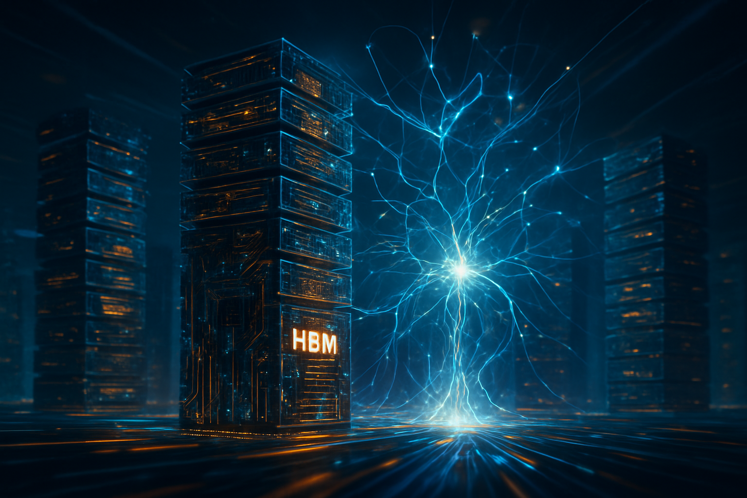
    The significance of these numbers cannot be overstated. As of late December 2025, it has become clear that memory is no longer a peripheral component of the AI stack; it is the fundamental "oxygen" that allows AI accelerators to breathe. Micron’s announcement that its High Bandwidth Memory (HBM) capacity for the entire 2026 calendar year is already sold out highlights a critical bottleneck in the global AI supply chain. With major hyperscalers locked into long-term agreements, the industry is entering an era where the ability to compute is strictly governed by the ability to store and move data at lightning speeds.

    The Technical Evolution: From HBM3E to the HBM4 Frontier

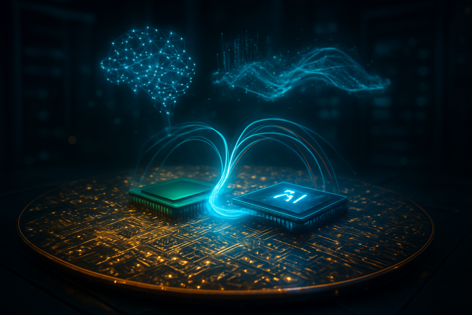
    The technical drivers behind Micron’s record-breaking quarter lie in the rapid adoption of HBM3E and the impending transition to HBM4. High Bandwidth Memory is uniquely engineered to provide the massive data throughput required by modern Large Language Models (LLMs). Unlike traditional DDR5 memory, HBM stacks DRAM dies vertically and connects them directly to the processor using a silicon interposer. Micron’s current HBM3E 12-high stacks offer industry-leading power efficiency and bandwidth, but the demand has already outpaced the company’s ability to manufacture them.

    The manufacturing process for HBM is notoriously "wafer-intensive." For every bit of HBM produced, approximately three bits of standard DRAM capacity are lost due to the complexity of the stacking and through-silicon via (TSV) processes. This "capacity asymmetry" is a primary reason for the persistent supply crunch. Furthermore, AI servers now require six to eight times more DRAM than conventional enterprise servers, creating a multiplier effect on demand that the industry has never seen before.

    Looking ahead, the shift toward HBM4 is slated for mid-2026. This next generation of memory is expected to offer bandwidth exceeding 2.0 TB/s per stack—a 60% improvement over HBM3E—while utilizing a 12nm logic process. This transition represents a significant architectural shift, as HBM4 will increasingly blur the lines between memory and logic, allowing for even tighter integration with next-generation AI accelerators.

    A New Competitive Landscape for Tech Giants

    The "sold out" status of Micron’s 2026 capacity creates a complex strategic environment for the world’s largest tech companies. NVIDIA (NASDAQ: NVDA), Meta Platforms (NASDAQ: META), and Microsoft (NASDAQ: MSFT) are currently in a high-stakes race to secure enough HBM to power their upcoming data center expansions. Because Micron can currently only fulfill about half to two-thirds of the requirements for some of its largest customers, these tech giants are forced to navigate a "scarcity economy" for silicon.

    For NVIDIA, Micron’s roadmap is particularly vital. Micron has already begun sampling its 36GB HBM4 modules, which are positioned as the primary memory solution for NVIDIA’s upcoming Vera Rubin AI architecture. This partnership gives Micron a strategic advantage over competitors like SK Hynix and Samsung, as it solidifies its role as a preferred supplier for the most advanced AI chips on the planet.

    Meanwhile, startups and smaller AI labs may find themselves at a disadvantage. As the "big three" memory producers (Micron, SK Hynix, and Samsung) prioritize high-margin HBM for hyperscalers, the availability of standard DRAM for other sectors could tighten, driving up costs across the entire electronics industry. This market positioning has led analysts at JPMorgan Chase (NYSE: JPM) and Morgan Stanley (NYSE: MS) to suggest that "Memory is the New Compute," shifting the power dynamics of the semiconductor sector.

    The Structural Shift: Why This Cycle is Different

    The term "AI Memory Supercycle" describes a structural shift in the industry rather than a typical boom-and-bust commodity cycle. Historically, the memory market has been plagued by volatility, with periods of oversupply leading to price crashes. However, the current environment is driven by multi-year infrastructure build-outs that are less sensitive to consumer spending and more tied to the fundamental race for AGI (Artificial General Intelligence).

    The wider significance of Micron's $13.64 billion quarter is the realization that the Total Addressable Market (TAM) for HBM is expanding much faster than anticipated. Micron now expects the HBM market to reach $100 billion by 2028, a milestone previously not expected until 2030 or later. This accelerated timeline suggests that the integration of AI into every facet of enterprise software and consumer technology is happening at a breakneck pace.

    However, this growth is not without concerns. The extreme capital intensity required to build new fabs—Micron has raised its FY2026 CapEx to $20 billion—means that the barrier to entry is higher than ever. There are also potential risks regarding the geographic concentration of manufacturing, though Micron’s expansion into Idaho and Syracuse, New York, supported by the CHIPS Act, provides a degree of domestic supply chain security that is increasingly valuable in the current geopolitical climate.

    Future Horizons: The Road to Mid-2026 and Beyond

    As we look toward the middle of 2026, the primary focus will be the mass production ramp of HBM4. This transition will be the most significant technical hurdle for the industry in years, as it requires moving to more advanced logic processes and potentially adopting "base die" customization where the memory is tailored specifically for the processor it sits next to.

    Beyond HBM, we are likely to see the emergence of new memory architectures like CXL (Compute Express Link), which allows for memory pooling across data centers. This could help alleviate some of the supply pressures by allowing for more efficient use of existing resources. Experts predict that the next eighteen months will be defined by "co-engineering," where memory manufacturers like Micron work hand-in-hand with chip designers from the earliest stages of development.

    The challenge for Micron will be executing its massive capacity expansion without falling into the traps of the past. Building the Syracuse and Idaho fabs is a multi-year endeavor that must perfectly time the market's needs. If AI demand remains on its current trajectory, even these massive investments may only barely keep pace with the world's hunger for data.

    Final Reflections on a Watershed Moment

    Micron’s fiscal Q1 2026 results represent a watershed moment in AI history. By shattering revenue records and guiding for an even more explosive Q2, the company has proved that the AI revolution is as much about the "bits" of memory as it is about the "flops" of processing power. The fact that 2026 capacity is already spoken for is the ultimate validation of the AI Memory Supercycle.

    For investors and industry observers, the key takeaway is that the bottleneck for AI progress has shifted. While GPU availability was the story of 2024 and 2025, the narrative of 2026 will be defined by HBM supply. Micron has successfully transformed itself from a cyclical commodity producer into a high-tech cornerstone of the global AI economy.

    In the coming weeks, all eyes will be on how competitors respond and whether the supply chain can keep up with the $18.7 billion quarterly demand Micron has forecasted. One thing is certain: the era of "Memory as the New Compute" has officially arrived, and Micron Technology is leading the charge.


    This content is intended for informational purposes only and represents analysis of current AI developments.

    TokenRing AI delivers enterprise-grade solutions for multi-agent AI workflow orchestration, AI-powered development tools, and seamless remote collaboration platforms.
    For more information, visit https://www.tokenring.ai/.

  • Sustainability in the Fab: The Race for Net-Zero Water and Energy

    Sustainability in the Fab: The Race for Net-Zero Water and Energy

    As the artificial intelligence "supercycle" continues to accelerate, driving global chip sales to a record $72.7 billion in October 2025, the semiconductor industry is facing an unprecedented resource crisis. The transition to 2nm and 1.4nm manufacturing nodes has proven to be a double-edged sword: while these chips power the next generation of generative AI, their production requires up to 2.3 times more water and 3.5 times more electricity than previous generations. In response, the world’s leading foundries have transformed their operations, turning the "mega-fab" into a laboratory for radical sustainability and "Net-Zero" resource management.

    This shift has moved beyond corporate social responsibility into the realm of operational necessity. In late 2025, water scarcity in hubs like Arizona and Taiwan has made "Net-Positive" water status—where a company returns more water to the ecosystem than it withdraws—the new gold standard for the industry. From Micron’s billion-dollar conservation funds to TSMC’s pioneering reclaimed water plants, the race to build the first truly circular semiconductor ecosystem is officially on, powered by the very AI these facilities were built to produce.

    The Technical Frontiers of Ultrapure Water and Zero Liquid Discharge

    At the heart of the sustainability push is the management of Ultrapure Water (UPW), a substance thousands of times cleaner than pharmaceutical-grade water. In the 2nm era, even a "killer particle" as small as 10nm can ruin a wafer, making the purification process more intensive than ever. To combat the waste associated with this purity, companies like Micron Technology (NASDAQ: MU) have committed to a $1 billion sustainability initiative. As of late 2025, Micron has already deployed over $406 million of this fund, achieving a 66% global water conservation rate. Their planned $100 billion mega-fab in Clay, New York, is currently implementing a "Green CHIPS" framework designed to achieve near-100% water conservation through massive internal recycling loops.

    Taiwan Semiconductor Manufacturing Company (NYSE: TSM), or TSMC, has taken a different but equally ambitious path with its industrial-scale reclaimed water plants. In Taiwan’s Southern Taiwan Science Park, TSMC’s facilities reached a milestone in 2025, supplying nearly 67,000 metric tons of recycled water daily. Meanwhile, at its Phoenix, Arizona campus, TSMC broke ground in August 2025 on a new 15-acre Industrial Reclamation Water Plant (IRWP). Once fully operational, this facility is designed to recycle 90% of the fab's industrial wastewater, reducing the daily demand of a single fab from 4.75 million gallons to under 1.2 million gallons—a critical achievement in the water-stressed American Southwest.

    Technologically, these "Net-Zero" systems rely on a complex hierarchy of purification. Modern fabs in 2025 utilize segmented waste streams, separating chemical rinses from hydrofluoric acid waste to treat them individually. Advanced techniques such as Pulse-Flow Reverse Osmosis (PFRO) and Electrodeionization (EDI) are now standard, allowing for 98% water recovery. Furthermore, the introduction of 3D-printed spacers in membrane filtration—a technology backed by Micron—has significantly reduced the energy required to push water through these microscopic filters, addressing the energy-water nexus head-on.

    Competitive Advantages and the Rise of 'Green' Silicon

    The push for sustainability is reshaping the competitive landscape for chipmakers like Intel (NASDAQ: INTC) and Samsung Electronics (KRX: 005930). Intel’s Q4 2025 update confirmed that its 18A (1.8nm) process node is not just a performance leader but a sustainability one, delivering a 40% reduction in power consumption compared to older nodes. By simplifying the processing flow by 44% through advanced EUV lithography, Intel has reduced the total material intensity of its most advanced chips. This "green silicon" approach provides a strategic advantage as major customers like Microsoft (NASDAQ: MSFT) and NVIDIA (NASDAQ: NVDA) now demand verified "carbon and water receipts" for every wafer to meet their own 2030 net-zero goals.

    Samsung has countered with its own massive milestones, announcing in October 2025 that it achieved the UL Solutions "Zero Waste to Landfill" Platinum designation across all its global manufacturing sites. In South Korea, Samsung’s collaboration with the Ministry of Environment now supplies 120,000 tonnes of reclaimed water per day to its Giheung and Hwaseong fabs. For these giants, sustainability is no longer just about compliance; it is a market positioning tool. Foundries that can guarantee production continuity in water-stressed regions while lowering the carbon footprint of the end product are winning the lion's share of long-term supply contracts from sustainability-conscious tech titans.

    AI as the Architect of the Sustainable Fab

    Perhaps the most poetic development of 2025 is the use of AI to optimize the very factories that create it. "Agentic AI" ecosystems, such as those launched by Schneider Electric (EPA: SU) in mid-2025, now act as autonomous stewards of fab resources. these AI agents monitor thousands of sensors in real-time, making independent adjustments to chiller settings, HVAC airflow, and ultrapure water flow rates. This has led to an average 20% improvement in operational energy efficiency across modern mega-fabs.

    Digital Twin technology has also become a standard requirement for new construction. Companies like Applied Materials (NASDAQ: AMAT) are utilizing their EPIC platform to create high-fidelity virtual replicas of the manufacturing process. By simulating gas usage and chemical reactions before a single wafer is processed, these AI-driven systems have achieved a 50% reduction in gas usage and significantly reduced wafer scrap. This "yield-as-sustainability" metric is crucial; by reducing the number of defective chips, fabs indirectly save millions of gallons of water and megawatts of power that would have been "wasted" on failed silicon.

    The Road to 2030: Challenges and Next Steps

    Looking ahead, the industry faces the daunting task of scaling these "Net-Zero" successes as they move toward 1.4nm and 1nm nodes. While 90% water recycling is achievable today, the final 10%—often referred to as the "brine challenge"—remains difficult and energy-intensive to treat. Experts predict that the next three years will see a surge in investment toward Zero Liquid Discharge (ZLD) technologies that can evaporate and crystallize the final waste streams into solid minerals, leaving no liquid waste behind.

    Furthermore, the integration of AI into the power grid itself is a major focus for 2026. The U.S. Department of Energy’s "Genesis Mission," launched in December 2025, aims to use AI to coordinate the massive energy demands of semiconductor clusters with renewable energy availability. As fabs become larger and more complex, the ability to "load-balance" a mega-fab against a city’s power grid will be the next great frontier in industrial AI applications.

    A New Era for Semiconductor Manufacturing

    The semiconductor industry's evolution in 2025 marks a definitive end to the era of "growth at any cost." The race for Net-Zero water and energy has proven that high-performance computing and environmental stewardship are not mutually exclusive. Through a combination of radical transparency, multi-billion dollar infrastructure investments, and the deployment of agentic AI, the industry is setting a blueprint for how heavy industry can adapt to a resource-constrained world.

    As we move into 2026, the focus will shift from building these sustainable systems to proving their long-term resilience. The success of TSMC’s Arizona plant and Micron’s New York mega-fab will be the ultimate litmus test for the industry's green ambitions. For now, the "Sustainability in the Fab" movement has demonstrated that the most important breakthrough in the AI era might not be the chips themselves, but the sustainable way in which we make them.


    This content is intended for informational purposes only and represents analysis of current AI developments.

    TokenRing AI delivers enterprise-grade solutions for multi-agent AI workflow orchestration, AI-powered development tools, and seamless remote collaboration platforms.
    For more information, visit https://www.tokenring.ai/.

  • India’s Silicon Century: Micron’s Sanand Facility Ramps Up as Semiconductor Mission Hits $18 Billion Milestone

    India’s Silicon Century: Micron’s Sanand Facility Ramps Up as Semiconductor Mission Hits $18 Billion Milestone

    As 2025 draws to a close, India’s ambitious journey to become a global semiconductor powerhouse has reached a definitive turning point. Micron Technology, Inc. (NASDAQ: MU) has officially completed the civil construction of its landmark Assembly, Test, Marking, and Packaging (ATMP) facility in Sanand, Gujarat. This milestone marks the transition of the $2.75 billion project from a high-stakes construction site to a live operational hub, signaling the first major success of the India Semiconductor Mission (ISM). With cleanrooms validated and advanced machinery now humming, the facility is preparing for high-volume commercial production in early 2026, positioning India as a critical node in the global memory chip supply chain.

    The progress at Sanand is not an isolated success but the centerpiece of a broader industrial awakening. As of December 2025, the ISM has successfully catalyzed a cumulative investment of $18.2 billion across ten major approved projects. From the massive 300mm wafer fab being erected by Tata Electronics in Dholera to the operational pilot lines of the CG Power and Industrial Solutions Ltd (NSE: CGPOWER) and Renesas Electronics Corp (TYO: 6723) joint venture, the Indian landscape is being physically reshaped by the "Silicon Century." This rapid industrialization represents one of the most significant shifts in the global technology hardware sector in decades, directly challenging established hubs in East Asia.

    Engineering the Future: Technical Feats at Sanand and Dholera

    The Micron Sanand facility is a marvel of modern modular engineering, a first for the company’s global operations. Spanning 93 acres with a built-up area of 1.4 million square feet, the plant utilized a "modularization strategy" where massive structural sections—some weighing over 700 tonnes—were pre-assembled and lifted into place using precision strand jacks. This approach allowed Micron to complete the Phase 1 structure in record time despite the complexities of building a Class 100 cleanroom. The facility is now entering its final equipment calibration phase, utilizing Zero Liquid Discharge (ZLD) technology to ensure sustainability in the arid Gujarat climate, a technical requirement that has become a blueprint for future Indian fabs.

    Further north in Dholera, Tata Electronics is making parallel strides with its $11 billion mega-fab, partnered with Powerchip Semiconductor Manufacturing Corp (TPE: 6770). As of late 2025, the primary building structures are complete, and the project has moved into the "Advanced Equipment Installation" phase. This facility is designed to process 300mm (12-inch) wafers, targeting mature nodes between 28nm and 110nm. These nodes are the workhorses of the automotive, power management, and IoT sectors. Initial pilot runs for "Made-in-India" logic chips are expected to emerge from the Dholera lines by the end of this month, marking the first time a commercial-grade silicon wafer has been processed on Indian soil.

    The technical ecosystem is further bolstered by the inauguration of the G1 facility in Sanand by the CG Power-Renesas-Stars Microelectronics joint venture. This unit serves as India’s first end-to-end OSAT (Outsourced Semiconductor Assembly and Test) pilot line to reach operational status. With a capacity of 0.5 million units per day, the G1 facility is already undergoing customer qualification trials for chips destined for 5G infrastructure and electric vehicles. The speed at which these facilities have moved from groundbreaking to equipment installation has surprised global industry experts, who initially viewed India’s 2021 semiconductor policy as overly optimistic.

    Shifting Tides: Impact on Tech Giants and the Global Supply Chain

    The operationalizing of these facilities is already causing a ripple effect across the boardrooms of global tech giants. Apple Inc. (NASDAQ: AAPL), which now sources approximately 20% of its global iPhone output from India, stands as a primary beneficiary. Localized semiconductor packaging and eventual fabrication will allow Apple and its manufacturing partners, such as Foxconn, to further reduce lead times and logistics costs. Similarly, Samsung Electronics (KRX: 005930) has continued to pivot its production focus toward its massive Noida hub, viewing India's emerging chip ecosystem as a hedge against geopolitical volatility in the Taiwan Strait and the ongoing tech decoupling from China.

    For the incumbent semiconductor leaders, India’s rise presents a new competitive theater. While the current focus is on "legacy" nodes and backend packaging, the strategic advantage lies in the "China+1" strategy. Major AI labs and tech companies are increasingly looking to diversify their hardware dependencies. The presence of Micron and Tata Electronics provides a viable alternative for high-volume, cost-sensitive components. This shift is also empowering a new generation of Indian fabless startups. Under the Design Linked Incentive (DLI) scheme, over 70 startups are now designing indigenous processors, such as the DHRUV64, which will eventually be manufactured in the very fabs now rising in Dholera and Sanand.

    The market positioning of these new Indian facilities is focused on the "middle of the pyramid"—the high-volume chips that power the world's appliances, cars, and smartphones. By securing the packaging and mature-node fabrication segments first, India is building the foundational expertise required to eventually compete in the sub-7nm "leading-edge" space. This strategic patience has earned the respect of the industry, as it avoids the "white elephant" projects that have plagued other nations' attempts to enter the semiconductor market.

    A Geopolitical Pivot: India’s Role in the Global Landscape

    The completion of Micron’s civil work and the $18 billion investment milestone are more than just industrial achievements; they are geopolitical statements. In the broader AI and technology landscape, hardware sovereignty has become as crucial as software prowess. India’s successful execution of the ISM projects by late 2025 places it in an elite group of nations capable of hosting complex semiconductor manufacturing. This development mirrors previous milestones like the rise of Taiwan’s TSMC in the 1980s or South Korea’s memory boom in the 1990s, though India is attempting this transition at a significantly faster pace.

    However, the rapid expansion has not been without concerns. The massive requirements for ultrapure water and stable, high-voltage electricity have forced the Gujarat and Assam state governments to invest billions in dedicated utility corridors. Environmentalists have raised questions regarding the long-term impact of semiconductor manufacturing on local water tables, prompting companies like Micron to adopt world-class recycling technologies. Despite these challenges, the consensus among global analysts is that India’s entry into the semiconductor value chain is a "net positive" for global supply chain resilience, reducing the world's over-reliance on a few concentrated geographic zones.

    Comparing this to previous AI and tech milestones, the "ramping of Sanand" is being viewed as the hardware equivalent of India's IT services boom in the late 1990s. While the software era made India the "back office" of the world, the semiconductor era aims to make it the "engine room." The integration of AI-driven manufacturing processes within these new fabs is also a notable trend, with Micron utilizing advanced AI for defect detection and yield optimization, further bridging the gap between India's software expertise and its new hardware ambitions.

    The Road Ahead: What’s Next for the India Semiconductor Mission?

    Looking toward 2026 and beyond, the focus will shift from "building" to "yielding." The immediate priority for Micron will be the successful ramp-up of commercial shipments to global markets, while Tata Electronics will aim to move from pilot runs to high-volume 300mm wafer production. Experts predict that the next phase of the ISM will involve attracting a "leading-edge" fab (sub-10nm) and expanding the domestic ecosystem for semiconductor grade chemicals and gases. The government is expected to announce "ISM 2.0" in early 2026, which may include expanded fiscal support to reach a total investment target of $50 billion by 2030.

    Potential applications on the horizon include the domestic manufacturing of AI accelerators and specialized chips for India’s burgeoning space and defense sectors. Challenges remain, particularly in the realm of talent acquisition. While India has a massive pool of chip designers, the specialized workforce required for "cleanroom operations" and "wafer fabrication" is still being developed through intensive training programs in collaboration with universities in the US and Taiwan. The success of these talent pipelines will be the ultimate factor in determining the long-term sustainability of the Dholera and Sanand clusters.

    Conclusion: A New Era of Indian Electronics

    The progress of the India Semiconductor Mission in late 2025 represents a historic triumph of policy and industrial execution. The completion of Micron’s Sanand facility and the rapid advancement of Tata’s Dholera fab are the tangible fruits of an $18 billion gamble that many doubted would pay off. These facilities are no longer just blueprints; they are the physical foundations of a self-reliant digital economy that will influence the global technology landscape for decades to come.

    As we move into 2026, the world will be watching the first commercial exports of memory chips from Sanand and the first logic chips from Dholera. These milestones will serve as the final validation of India’s place in the global semiconductor hierarchy. For the tech industry, the message is clear: the global supply chain has a new, formidable anchor in the Indian subcontinent. The "Silicon Century" has truly begun, and its heart is beating in the industrial corridors of Gujarat.


    This content is intended for informational purposes only and represents analysis of current AI developments.

    TokenRing AI delivers enterprise-grade solutions for multi-agent AI workflow orchestration, AI-powered development tools, and seamless remote collaboration platforms.
    For more information, visit https://www.tokenring.ai/.

  • Micron’s AI Supercycle: Record $13.6B Revenue Fueled by HBM4 Dominance

    Micron’s AI Supercycle: Record $13.6B Revenue Fueled by HBM4 Dominance

    The artificial intelligence revolution has officially entered its next phase, moving beyond the processors themselves to the high-performance memory that feeds them. On December 17, 2025, Micron Technology, Inc. (NASDAQ: MU) stunned Wall Street with a record-breaking Q1 2026 earnings report that solidified its position as a linchpin of the global AI infrastructure. Reporting a staggering $13.64 billion in revenue—a 57% increase year-over-year—Micron has proven that the "AI memory super-cycle" is not just a trend, but a fundamental shift in the semiconductor landscape.

    This financial milestone is driven by the insatiable demand for High Bandwidth Memory (HBM), specifically the upcoming HBM4 standard, which is now being treated as a strategic national asset. As data centers scramble to support increasingly massive large language models (LLMs) and generative AI applications, Micron’s announcement that its HBM supply for the entirety of 2026 is already fully sold out has sent a clear signal to the industry: the bottleneck for AI progress is no longer just compute power, but the ability to move data fast enough to keep that power utilized.

    The HBM4 Paradigm Shift: More Than Just an Upgrade

    The technical specifications revealed during the Q1 earnings call highlight why HBM4 is being hailed as a "paradigm shift" rather than a simple generational improvement. Unlike HBM3E, which utilized a 1,024-bit interface, HBM4 doubles the interface width to 2,048 bits. This change allows for a massive leap in bandwidth, reaching up to 2.8 TB/s per stack. Furthermore, Micron is moving toward the normalization of 16-Hi stacks, a feat of precision engineering that allows for higher density and capacity in a smaller footprint.

    Perhaps the most significant technical evolution is the transition of the base die from a standard memory process to a logic process (utilizing 12nm or even 5nm nodes). This convergence of memory and logic allows for superior IOPS per watt, enabling the memory to run a wider bus at a lower frequency to maintain thermal efficiency—a critical factor for the next generation of AI accelerators. Industry experts have noted that this architecture is specifically designed to feed the upcoming "Rubin" GPU architecture from NVIDIA Corporation (NASDAQ: NVDA), which requires the extreme throughput that only HBM4 can provide.

    Reshaping the Competitive Landscape of Silicon Valley

    Micron’s performance has forced a reevaluation of the competitive dynamics between the "Big Three" memory makers: Micron, SK Hynix, and Samsung Electronics (KRX: 005930). By securing a definitive "second source" status for NVIDIA’s most advanced chips, Micron is well on its way to capturing its targeted 20%–25% share of the HBM market. This shift is particularly disruptive to existing products, as the high margins of HBM (expected to keep gross margins in the 60%–70% range) allow Micron to pivot away from the more volatile and sluggish consumer PC and smartphone markets.

    Tech giants like Meta Platforms, Inc. (NASDAQ: META), Microsoft Corp (NASDAQ: MSFT), and Alphabet Inc. (NASDAQ: GOOGL) stand to benefit—and suffer—from this development. While the availability of HBM4 will enable more powerful AI services, the "fully sold out" status through 2026 creates a high-stakes environment where access to memory becomes a primary strategic advantage. Companies that did not secure long-term supply agreements early may find themselves unable to scale their AI hardware at the same pace as their competitors.

    The $100 Billion Horizon and National Security

    The wider significance of Micron’s report lies in its revised market forecast. CEO Sanjay Mehrotra announced that the HBM Total Addressable Market (TAM) is now projected to hit $100 billion by 2028—a milestone reached two years earlier than previous estimates. This explosive growth underscores how central memory has become to the broader AI landscape. It is no longer a commodity; it is a specialized, high-tech component that dictates the ceiling of AI performance.

    This shift has also taken on a geopolitical dimension. The U.S. government recently reallocated $1.2 billion in support to fast-track Micron’s domestic manufacturing sites, classifying HBM4 as a strategic national asset. This move reflects a broader trend of "onshoring" critical technology to ensure supply chain resilience. As memory becomes as vital as oil was in the 20th century, the expansion of domestic capacity in Idaho and New York is seen as a necessary step for national economic security, mirroring the strategic importance of the original CHIPS Act.

    Mapping the $20 Billion Expansion and Future Challenges

    To meet this unprecedented demand, Micron has hiked its fiscal 2026 capital expenditure (CapEx) to $20 billion. A primary focus of this investment is the "Idaho Acceleration" project, with the first new fab expected to produce wafers by mid-2027 and a second site by late 2028. Beyond the U.S., Micron is expanding its global footprint with a $9.6 billion fab in Hiroshima, Japan, and advanced packaging operations in Singapore and India. This massive investment aims to solve the capacity crunch, but it comes with significant engineering hurdles.

    The primary challenge moving forward will be yield rates. As HBM4 moves to 16-Hi stacks, the manufacturing complexity increases exponentially. A single defect in just one of the 16 layers can render the entire stack useless, leading to potentially high waste and lower-than-expected output in the early stages of mass production. Experts predict that the "yield war" of 2026 will be the next major story in the semiconductor industry, as Micron and its rivals race to perfect the bonding processes required for these vertical skyscrapers of silicon.

    A New Era for the Memory Industry

    Micron’s Q1 2026 earnings report marks a definitive turning point in semiconductor history. The transition from $13.64 billion in quarterly revenue to a projected $100 billion annual market for HBM by 2028 signals that the AI era is still in its early innings. Micron has successfully transformed itself from a provider of commodity storage into a high-margin, indispensable partner for the world’s most advanced AI labs.

    As we move into 2026, the industry will be watching two key metrics: the progress of the Idaho fab construction and the initial yield rates of the HBM4 mass production scheduled for the second quarter. If Micron can execute on its $20 billion expansion plan while maintaining its technical lead, it will not only secure its own future but also provide the essential foundation upon which the next generation of artificial intelligence will be built.


    This content is intended for informational purposes only and represents analysis of current AI developments.

    TokenRing AI delivers enterprise-grade solutions for multi-agent AI workflow orchestration, AI-powered development tools, and seamless remote collaboration platforms.
    For more information, visit https://www.tokenring.ai/.

  • The Silicon Backbone: How the AI Revolution Triggered a $52 Billion Semiconductor Talent War

    The Silicon Backbone: How the AI Revolution Triggered a $52 Billion Semiconductor Talent War

    As the global race for artificial intelligence supremacy accelerates, the industry has hit a formidable and unexpected bottleneck: a critical shortage of the human experts required to build the hardware that powers AI. As of late 2025, the United States semiconductor industry is grappling with a staggering "talent war," characterized by more than 25,000 immediate job openings across the "Silicon Desert" of Arizona and the "Silicon Heartland" of Ohio. This labor crisis threatens to derail the ambitious domestic manufacturing goals set by the CHIPS and Science Act, as the demand for 2nm and below processing nodes outstrips the supply of qualified engineers and technicians.

    The immediate significance of this development cannot be overstated. While the federal government has committed billions to build physical fabrication plants (fabs), the lack of a specialized workforce has turned into a primary risk factor for project timelines. From entry-level fab technicians to PhD-level Extreme Ultraviolet (EUV) lithography experts, the industry is pivoting away from traditional recruitment models toward aggressive "skills academies" and unprecedented university partnerships. This shift marks a fundamental restructuring of how the tech industry prepares its workforce for the era of hardware-defined AI.

    From Degrees to Certifications: The Rise of Semiconductor Skills Academies

    The current talent gap is not merely a numbers problem; it is a specialized skills mismatch. Of the 25,000+ current openings, a significant portion is for mid-level technicians who do not necessarily require a four-year engineering degree but do need highly specific training in cleanroom protocols and vacuum systems. To address this, industry leaders like Intel (NASDAQ:INTC) have pioneered "Quick Start" programs. In Arizona, Intel partnered with Maricopa Community Colleges to offer a two-week intensive program that transitions workers from adjacent industries—such as automotive or aerospace—into entry-level semiconductor roles.

    Technically, these programs are a departure from the "ivory tower" approach to engineering. They utilize "digital twin" training environments—virtual replicas of multi-billion dollar fabs—allowing students to practice complex maintenance on EUV machines without risking damage to actual equipment. This technical shift is supported by the National Semiconductor Technology Center (NSTC) Workforce Center of Excellence, which received a $250 million investment in early 2025 to standardize these digital training modules nationwide.

    Initial reactions from the AI research community have been cautiously optimistic. Experts note that while these "skills academies" can solve the technician shortage, the "brain drain" at the higher end of the spectrum—specifically in advanced packaging and circuit design—remains acute. The complexity of 2nm chip architectures requires a level of physics and materials science expertise that cannot be fast-tracked in a two-week boot camp, leading to a fierce bidding war for graduate-level talent.

    Corporate Giants and the Strategic Hunt for Human Capital

    The talent war has created a new competitive landscape where a company’s valuation is increasingly tied to its ability to secure a workforce. Intel (NASDAQ:INTC) has been the most aggressive, committing $100 million to its Semiconductor Education and Research Program (SERP). By embedding itself in the curriculum of eight leading Ohio universities, including Ohio State, Intel is effectively "pre-ordering" the next generation of graduates to staff its $20 billion manufacturing hub in Licking County.

    TSMC (NYSE:TSM) has followed a similar playbook in Arizona. By partnering with Arizona State University (ASU) through the CareerCatalyst platform, TSMC is leveraging non-degree, skills-based education to fill its Phoenix-based fabs. This move is a strategic necessity; TSMC’s expansion into the U.S. has been historically hampered by cultural and technical differences in workforce management. By funding local training centers, TSMC is attempting to build a "homegrown" workforce that can operate its most advanced 3nm and 2nm lines.

    Meanwhile, Micron (NASDAQ:MU) has looked toward international cooperation to solve the domestic shortage. Through the UPWARDS Network, a $60 million initiative involving Tokyo Electron (OTC:TOELY) and several U.S. and Japanese universities, Micron is cultivating a global talent pool. This cross-border strategy provides a competitive advantage by allowing Micron to tap into the specialized lithography expertise of Japanese engineers while training U.S. students at Purdue University and Virginia Tech.

    National Security and the Broader AI Landscape

    The semiconductor talent war is more than just a corporate HR challenge; it is a matter of national security and a critical pillar of the global AI landscape. The 2024-2025 surge in AI-specific chips has made it clear that the "software-first" mentality of the last decade is no longer sufficient. Without a robust workforce to operate domestic fabs, the U.S. remains vulnerable to supply chain disruptions that could freeze AI development overnight.

    This situation echoes previous milestones in tech history, such as the 1960s space race, where the government and private sector had to fundamentally realign the education system to meet a national objective. However, the current crisis is complicated by the fact that the semiconductor industry is competing for the same pool of STEM talent as the high-paying software and finance sectors. There are growing concerns that the "talent war" could lead to a cannibalization of other critical tech industries if not managed through a broad expansion of the total talent pool.

    Furthermore, the focus on "skills academies" and rapid certification raises questions about long-term innovation. While these programs fill the immediate 25,000-job gap, some industry veterans worry that a shift away from deep, fundamental research in favor of vocational training could slow the breakthrough discoveries needed for post-silicon computing or room-temperature superconductors.

    The Future of Silicon Engineering: Automation and Digital Twins

    Looking ahead to 2026 and beyond, the industry is expected to turn toward AI itself to solve the human talent shortage. "AI for EDA" (Electronic Design Automation) is a burgeoning field where machine learning models assist in the layout and verification of complex circuits, potentially reducing the number of human engineers required for a single project. We are also likely to see the expansion of "lights-out" manufacturing—fully automated fabs that require fewer human technicians on the floor, though this will only increase the demand for high-level software engineers to maintain the automation systems.

    In the near term, the success of the CHIPS Act will be measured by the graduation rates of programs like Purdue’s Semiconductor Degrees Program (SDP) and the STARS (Summer Training, Awareness, and Readiness for Semiconductors) initiative. Experts predict that if these university-corporate partnerships can bridge 50% of the projected 67,000-worker shortfall by 2030, the U.S. will have successfully secured its position as a global semiconductor powerhouse.

    A Decisive Moment for the Hardware Revolution

    The 25,000-job opening gap in the semiconductor industry is a stark reminder that the AI revolution is built on a foundation of physical hardware and human labor. The transition from traditional academic pathways to agile "skills academies" and deep corporate-university integration represents one of the most significant shifts in technical education in decades. As Intel, TSMC, and Micron race to staff their new facilities, the winners of the talent war will likely be the winners of the AI era.

    Key takeaways from this development include the critical role of federal funding in workforce infrastructure, the rising importance of "digital twin" training technologies, and the strategic necessity of regional talent hubs. In the coming months, industry watchers should keep a close eye on the first wave of graduates from the Intel-Ohio and TSMC-ASU partnerships. Their ability to seamlessly integrate into high-stakes fab environments will determine whether the U.S. can truly bring the silicon backbone of AI back to its own shores.


    This content is intended for informational purposes only and represents analysis of current AI developments.

    TokenRing AI delivers enterprise-grade solutions for multi-agent AI workflow orchestration, AI-powered development tools, and seamless remote collaboration platforms.
    For more information, visit https://www.tokenring.ai/.

  • The High-Bandwidth Bottleneck: Inside the 2025 Memory Race and the HBM4 Pivot

    The High-Bandwidth Bottleneck: Inside the 2025 Memory Race and the HBM4 Pivot

    As 2025 draws to a close, the artificial intelligence industry finds itself locked in a high-stakes "Memory Race" that has fundamentally shifted the economics of computing. In the final quarter of 2025, High-Bandwidth Memory (HBM) contract prices have surged by a staggering 30%, driven by an insatiable demand for the specialized silicon required to feed the next generation of AI accelerators. This price spike reflects a critical bottleneck: while GPU compute power has scaled exponentially, the ability to move data in and out of those processors—the "Memory Wall"—has become the primary constraint for trillion-parameter model training.

    The current market volatility is not merely a supply-demand imbalance but a symptom of a massive industrial pivot. As of December 24, 2025, the industry is aggressively transitioning from the current HBM3e standard to the revolutionary HBM4 architecture. This shift is being forced by the upcoming release of next-generation hardware like NVIDIA’s (NASDAQ: NVDA) Rubin architecture and AMD’s (NASDAQ: AMD) Instinct MI400 series, both of which require the massive throughput that only HBM4 can provide. With 2025 supply effectively sold out since mid-2024, the Q4 price surge highlights the desperation of AI cloud providers and enterprises to secure the memory needed for the 2026 deployment cycle.

    Doubling the Pipes: The Technical Leap to HBM4

    The transition to HBM4 represents the most significant architectural overhaul in the history of stacked memory. Unlike previous generations which offered incremental speed bumps, HBM4 doubles the memory interface width from 1024-bit to 2048-bit. This "wider is better" approach allows for massive bandwidth gains—reaching up to 2.8 TB/s per stack—without requiring the extreme clock speeds that lead to overheating. By moving to a wider bus, manufacturers can maintain lower data rates per pin (around 6.4 to 8.0 Gbps) while still nearly doubling the total throughput compared to HBM3e.

    A pivotal technical development in 2025 was the JEDEC Solid State Technology Association’s decision to relax the package thickness specification to 775 micrometers (μm). This change has allowed the "Big Three" memory makers to utilize 16-high (16-Hi) stacks using existing bonding technologies like Advanced MR-MUF (Mass Reflow Molded Underfill). Furthermore, HBM4 introduces the "logic base die," where the bottom layer of the memory stack is manufactured using advanced logic processes from foundries like TSMC (NYSE: TSM). This allows for direct integration of custom features and improved thermal management, effectively blurring the line between memory and the processor itself.

    Initial reactions from the AI research community have been a mix of relief and concern. While the throughput of HBM4 is essential for the next leap in Large Language Models (LLMs), the complexity of these 16-layer stacks has led to lower yields than previous generations. Experts at the 2025 International Solid-State Circuits Conference noted that the integration of logic dies requires unprecedented cooperation between memory makers and foundries, creating a new "triangular alliance" model of semiconductor manufacturing that departs from the traditional siloed approach.

    Market Dominance and the "One-Stop Shop" Strategy

    The memory race has reshaped the competitive landscape for the world’s leading semiconductor firms. SK Hynix (KRX: 000660) continues to hold a dominant market share, exceeding 50% in the HBM segment. Their early partnership with NVIDIA and TSMC has given them a first-mover advantage, with SK Hynix shipping the first 12-layer HBM4 samples in late 2025. Their "Advanced MR-MUF" technology has proven to be a reliable workhorse, allowing them to scale production faster than competitors who initially bet on more complex bonding methods.

    However, Samsung Electronics (KRX: 005930) has staged a formidable comeback in late 2025 by leveraging its unique position as a "one-stop shop." Samsung is the only company capable of providing HBM design, logic die foundry services, and advanced packaging all under one roof. This vertical integration has allowed Samsung to win back significant orders from major AI labs looking to simplify their supply chains. Meanwhile, Micron Technology (NASDAQ: MU) has carved out a lucrative niche by positioning itself as the power-efficiency leader. Micron’s HBM4 samples reportedly consume 30% less power than the industry average, a critical selling point for data center operators struggling with the cooling requirements of massive AI clusters.

    The financial implications for these companies are profound. To meet HBM demand, manufacturers have reallocated up to 30% of their standard DRAM wafer capacity to HBM production. This "capacity cannibalization" has not only fueled the 30% HBM price surge but has also caused a secondary price spike in consumer DDR5 and mobile LPDDR5X markets. For the memory giants, this represents a transition from a commodity-driven business to a high-margin, custom-silicon model that more closely resembles the logic chip industry.

    Breaking the Memory Wall in the Broader AI Landscape

    The urgency behind the HBM4 transition stems from a fundamental shift in the AI landscape: the move toward "Agentic AI" and trillion-parameter models that require near-instantaneous access to vast datasets. The "Memory Wall"—the gap between how fast a processor can calculate and how fast it can access data—has become the single greatest hurdle to achieving Artificial General Intelligence (AGI). HBM4 is the industry's most aggressive attempt to date to tear down this wall, providing the bandwidth necessary for real-time reasoning in complex AI agents.

    This development also carries significant geopolitical weight. As HBM becomes as strategically important as the GPUs themselves, the concentration of production in South Korea (SK Hynix and Samsung) and the United States (Micron) has led to increased government scrutiny of supply chain resilience. The 30% price surge in Q4 2025 has already prompted calls for more diversified manufacturing, though the extreme technical barriers to entry for HBM4 make it unlikely that new players will emerge in the near term.

    Furthermore, the energy implications of the memory race cannot be ignored. While HBM4 is more efficient per bit than its predecessors, the sheer volume of memory being packed into each server rack is driving data center power density to unprecedented levels. A single NVIDIA Rubin GPU is expected to feature up to 12 HBM4 stacks, totaling over 400GB of VRAM per chip. Scaling this across a cluster of tens of thousands of GPUs creates a power and thermal challenge that is pushing the limits of liquid cooling and data center infrastructure.

    The Horizon: HBM4e and the Path to 2027

    Looking ahead, the roadmap for high-bandwidth memory shows no signs of slowing down. Even as HBM4 begins its volume ramp-up in early 2026, the industry is already looking toward "HBM4e" and the eventual adoption of Hybrid Bonding. Hybrid Bonding will eliminate the need for traditional "bumps" between layers, allowing for even tighter stacking and better thermal performance, though it is not expected to reach high-volume manufacturing until 2027.

    In the near term, we can expect to see more "custom HBM" solutions. Instead of buying off-the-shelf memory stacks, hyperscalers like Google and Amazon may work directly with memory makers to customize the logic base die of their HBM4 stacks to optimize for specific AI workloads. This would further blur the lines between memory and compute, leading to a more heterogeneous and specialized hardware ecosystem. The primary challenge remains yield; as stack heights reach 16 layers and beyond, the probability of a single defective die ruining an entire expensive stack increases, making quality control the ultimate arbiter of success.

    A Defining Moment in Semiconductor History

    The Q4 2025 memory price surge and the subsequent HBM4 pivot mark a defining moment in the history of the semiconductor industry. Memory is no longer a supporting player in the AI revolution; it is now the lead actor. The 30% price hike is a clear signal that the "Memory Race" is the new front line of the AI war, where the ability to manufacture and secure advanced silicon is the ultimate competitive advantage.

    As we move into 2026, the industry will be watching the production yields of HBM4 and the initial performance benchmarks of NVIDIA’s Rubin and AMD’s MI400. The success of these platforms—and the continued evolution of AI itself—depends entirely on the industry's ability to scale these complex, 2048-bit memory "superhighways." For now, the message from the market is clear: in the era of generative AI, bandwidth is the only currency that matters.


    This content is intended for informational purposes only and represents analysis of current AI developments.

    TokenRing AI delivers enterprise-grade solutions for multi-agent AI workflow orchestration, AI-powered development tools, and seamless remote collaboration platforms.
    For more information, visit https://www.tokenring.ai/.

  • The HBM Gold Rush: Samsung and SK Hynix Pivot to HBM4 as Prices Soar

    The HBM Gold Rush: Samsung and SK Hynix Pivot to HBM4 as Prices Soar

    As 2025 draws to a close, the semiconductor landscape has been fundamentally reshaped by an insatiable hunger for artificial intelligence. What began as a surge in demand for GPUs has evolved into a full-scale "Gold Rush" for High-Bandwidth Memory (HBM), the critical silicon that feeds data to AI accelerators. Industry giants Samsung Electronics (KRX: 005930) and SK Hynix (KRX: 000660) are reporting record-breaking profit margins, fueled by a strategic pivot that is draining the supply of traditional DRAM to prioritize the high-margin HBM stacks required by the next generation of AI data centers.

    This week, as the industry looks toward 2026, the transition to the HBM4 standard has reached a fever pitch. With NVIDIA (NASDAQ: NVDA) preparing its upcoming "Rubin" architecture, the world’s leading memory makers are locked in a high-stakes race to qualify their 12-layer and 16-layer HBM4 samples. The financial stakes could not be higher: for the first time in history, memory manufacturers are reporting gross margins exceeding 60%, surpassing even the elite foundries they supply. This shift marks the end of the commodity era for memory, transforming DRAM into a specialized, high-performance compute platform.

    The Technical Leap to HBM4: Doubling the Pipe

    The HBM4 standard represents the most significant architectural shift in memory technology in a decade. Unlike the incremental transition from HBM3 to HBM3E, HBM4 doubles the interface width from 1024-bit to a massive 2048-bit bus. This "widening of the pipe" allows for unprecedented data transfer speeds, with SK Hynix and Micron Technology (NASDAQ: MU) demonstrating bandwidths exceeding 2.0 TB/s per stack. In practical terms, a single HBM4-equipped AI accelerator can process data at speeds that were previously only possible by combining multiple older-generation cards.

    One of the most critical technical advancements in late 2025 is the move toward 16-layer (16-Hi) stacks. Samsung has taken a technological lead in this area by committing to "bumpless" hybrid bonding. This manufacturing technique eliminates the traditional microbumps used to connect layers, allowing for thinner stacks and significantly improved thermal dissipation—a vital factor as AI chips generate increasingly intense heat. Meanwhile, SK Hynix has refined its Advanced Mass Reflow Molded Underfill (MR-MUF) process to maintain its dominance in yield and reliability, securing its position as the primary supplier for NVIDIA’s high-volume orders.

    Furthermore, the boundary between memory and logic is blurring. For the first time, memory makers are collaborating with Taiwan Semiconductor Manufacturing Company (NYSE: TSM) to manufacture the "base die" of the HBM stack on advanced 3nm and 5nm processes. This allows the memory controller to be integrated directly into the stack's base, offloading tasks from the main GPU and further increasing system efficiency. While SK Hynix and Micron have embraced this "one-team" approach with TSMC, Samsung is leveraging its unique position as both a memory maker and a foundry to offer a "turnkey" HBM4 solution, though it has recently opened the door to supporting TSMC-produced base dies to satisfy customer flexibility.

    Market Disruption: The Death of Cheap DRAM

    The pivot to HBM4 has sent shockwaves through the broader electronics market. To meet the demand for AI memory, Samsung, SK Hynix, and Micron have reallocated nearly 30% of their total DRAM wafer capacity to HBM production. Because HBM dies are significantly larger and more complex to manufacture than standard DDR5 or LPDDR5X chips, this shift has created a severe supply vacuum in the consumer and enterprise PC markets. As of December 2024, contract prices for traditional DRAM have surged by over 30% quarter-on-quarter, a trend that experts expect to continue well into 2026.

    For tech giants like Apple (NASDAQ: AAPL), Dell (NYSE: DELL), and HP (NYSE: HPQ), this means rising component costs for laptops and smartphones. However, the memory makers are largely indifferent to these pressures, as the margins on HBM are nearly triple those of commodity DRAM. SK Hynix recently posted record quarterly revenue of 24.45 trillion won, with HBM products accounting for a staggering 77% of its DRAM revenue. Samsung has seen a similar resurgence, with its Device Solutions division reclaiming the top spot in global memory revenue as its HBM4 prototypes passed qualification milestones in Q4 2025.

    This shift has also created a new competitive hierarchy. Micron, once considered a distant third in the HBM race, has successfully captured approximately 25% of the market by positioning itself as the power-efficiency leader. Micron’s HBM4 samples reportedly consume 30% less power than competing designs, a crucial selling point for hyperscalers like Microsoft (NASDAQ: MSFT) and Google (NASDAQ: GOOGL) who are struggling with the massive energy requirements of their AI clusters.

    The Broader AI Landscape: Infrastructure as the Bottleneck

    The HBM gold rush highlights a fundamental truth of the current AI era: the bottleneck is no longer just the logic of the GPU, but the ability to feed that logic with data. As LLMs (Large Language Models) grow in complexity, the "memory wall" has become the primary obstacle to performance. HBM4 is seen as the bridge that will allow the industry to move from 100-trillion parameter models to the quadrillion-parameter models expected in late 2026 and 2027.

    However, this concentration of production in South Korea and Taiwan has raised fresh concerns about supply chain resilience. With 100% of the world's HBM4 supply currently tied to just three companies and one primary foundry partner (TSMC), any geopolitical instability in the region could bring the global AI revolution to a grinding halt. This has led to increased pressure from the U.S. and European governments for these companies to diversify their advanced packaging facilities, resulting in Micron’s massive new investments in Idaho and Samsung’s expanded presence in Texas.

    Future Horizons: Custom HBM and Beyond

    Looking beyond the current HBM4 ramp-up, the industry is already eyeing "Custom HBM." In this upcoming phase, major AI players like Amazon (NASDAQ: AMZN) and Meta (NASDAQ: META) will no longer buy off-the-shelf memory. Instead, they will co-design the logic dies of their HBM stacks to include proprietary accelerators or security features. This will further entrench the partnership between memory makers and foundries, potentially leading to a future where memory and compute are fully integrated into a single 3D-stacked package.

    Experts predict that HBM4E will follow as early as 2027, pushing bandwidth even further. However, the immediate challenge remains scaling 16-layer production. Yields for these ultra-dense stacks remain lower than their 12-layer counterparts, and the industry must perfect hybrid bonding at scale to prevent overheating. If these hurdles are overcome, the AI data center of 2026 will possess an order of magnitude more memory bandwidth than the most advanced systems of 2024.

    Conclusion: A New Era of Silicon Dominance

    The transition to HBM4 represents more than just a technical upgrade; it is the definitive signal that the AI boom is a permanent structural shift in the global economy. Samsung, SK Hynix, and Micron have successfully pivoted from being suppliers of a commodity to being the gatekeepers of AI progress. Their record margins and sold-out capacity through 2026 reflect a market where performance is prized above all else, and price is no object for the titans of the AI industry.

    As we move into 2026, the key metrics to watch will be the mass-production yields of 16-layer HBM4 and the success of Samsung’s "turnkey" strategy versus the SK Hynix-TSMC alliance. For now, the message from Seoul and Boise is clear: the AI gold rush is only just beginning, and the memory makers are the ones selling the most expensive shovels in history.


    This content is intended for informational purposes only and represents analysis of current AI developments.

    TokenRing AI delivers enterprise-grade solutions for multi-agent AI workflow orchestration, AI-powered development tools, and seamless remote collaboration platforms. For more information, visit https://www.tokenring.ai/.

  • The High Bandwidth Memory Wars: SK Hynix’s 400-Layer Roadmap and the Battle for AI Data Centers

    The High Bandwidth Memory Wars: SK Hynix’s 400-Layer Roadmap and the Battle for AI Data Centers

    As of December 22, 2025, the artificial intelligence revolution has shifted its primary battlefield from the logic of the GPU to the architecture of the memory chip. In a year defined by unprecedented demand for AI data centers, the "High Bandwidth Memory (HBM) Wars" have reached a fever pitch. The industry’s leaders—SK Hynix (KRX: 000660), Samsung Electronics (KRX: 005930), and Micron Technology (NASDAQ: MU)—are locked in a relentless pursuit of vertical scaling, with SK Hynix recently establishing a mass production system for HBM4 and fast-tracking its 400-layer NAND roadmap to maintain its crown as the preferred supplier for the AI elite.

    The significance of this development cannot be overstated. As AI models like GPT-5 and its successors demand exponential increases in data throughput, the "memory wall"—the bottleneck where data transfer speeds cannot keep pace with processor power—has become the single greatest threat to AI progress. By successfully transitioning to next-generation stacking technologies and securing massive supply deals for projects like OpenAI’s "Stargate," these memory titans are no longer just component manufacturers; they are the gatekeepers of the next era of computing.

    Scaling the Vertical Frontier: 400-Layer NAND and HBM4 Technicals

    The technical achievement of 2025 is the industry's shift toward the 400-layer NAND threshold and the commercialization of HBM4. SK Hynix, which began mass production of its 321-layer 4D NAND earlier this year, has officially moved to a "Hybrid Bonding" (Wafer-to-Wafer) manufacturing process to reach the 400-layer milestone. This technique involves manufacturing memory cells and peripheral circuits on separate wafers before bonding them, a radical departure from the traditional "Peripheral Under Cell" (PUC) method. This shift is essential to avoid the thermal degradation and structural instability that occur when stacking over 300 layers directly onto a single substrate.

    HBM4 represents an even more dramatic leap. Unlike its predecessor, HBM3E, which utilized a 1024-bit interface, HBM4 doubles the bus width to 2048-bit. This allows for massive bandwidth increases even at lower clock speeds, which is critical for managing the heat generated by the latest NVIDIA (NASDAQ: NVDA) Rubin-class GPUs. SK Hynix’s HBM4 production system, finalized in September 2025, utilizes advanced Mass Reflow Molded Underfill (MR-MUF) packaging, which has proven to have superior heat dissipation compared to the Thermal Compression Non-Conductive Film (TC-NCF) methods favored by some competitors.

    Initial reactions from the AI research community have been overwhelmingly positive, particularly regarding SK Hynix’s new "AIN Family" (AI-NAND). The introduction of "High-Bandwidth Flash" (HBF) effectively treats NAND storage like HBM, allowing for massive capacity in AI inference servers that were previously limited by the high cost and lower density of DRAM. Experts note that this convergence of storage and memory is the first major architectural shift in data center design in over a decade.

    The Triad Tussle: Market Positioning and Competitive Strategy

    The competitive landscape in late 2025 has seen a dramatic narrowing of the gap between the "Big Three." SK Hynix remains the market leader, commanding approximately 55–60% of the HBM market and securing over 75% of initial HBM4 orders for NVIDIA’s upcoming Rubin platform. Their strategic partnership with Taiwan Semiconductor Manufacturing Company (NYSE: TSM) for HBM4 base dies has given them a distinct advantage in integration and yield.

    However, Samsung Electronics has staged a formidable comeback. After a difficult 2024, Samsung reportedly "topped" NVIDIA’s HBM4 performance benchmarks in December 2025, leveraging its "triple-stack" technology to reach 400-layer NAND density ahead of its rivals. Samsung’s ability to act as a "one-stop shop"—providing foundry, logic, and memory services—is beginning to appeal to hyperscalers like Meta and Google who are looking to reduce their reliance on the NVIDIA-TSMC-SK Hynix triumvirate.

    Micron Technology, while currently holding the third-place position with roughly 20-25% market share, has been the most aggressive in pricing and efficiency. Micron’s HBM3E (12-layer) was a surprise success in early 2025, though the company has faced reported yield challenges with its early HBM4 samples. Despite this, Micron’s deep ties with AMD and its focus on power-efficient designs have made it a critical partner for the burgeoning "sovereign AI" projects across Europe and North America.

    The Stargate Era: Wider Significance and the Global AI Landscape

    The broader significance of the HBM wars is most visible in the "Stargate" project—a $500 billion initiative by OpenAI and Microsoft to build the world's most powerful AI supercomputer. In late 2025, both Samsung and SK Hynix signed landmark letters of intent to supply up to 900,000 DRAM wafers per month for this project by 2029. This deal essentially guarantees that the next five years of memory production are already spoken for, creating a "permanent" supply crunch for smaller players and startups.

    This concentration of resources has raised concerns about the "AI Divide." With DRAM contract prices having surged between 170% and 500% throughout 2025, the cost of training and running large-scale models is becoming prohibitive for anyone not backed by a trillion-dollar balance sheet. Furthermore, the physical limits of stacking are forcing a conversation about power consumption. AI data centers now consume nearly 40% of global memory output, and the energy required to move data from memory to processor is becoming a major environmental hurdle.

    The HBM4 transition also marks a geopolitical shift. The announcement of "Stargate Korea"—a massive data center hub in South Korea—highlights how memory-producing nations are leveraging their hardware dominance to secure a seat at the table of AI policy and development. This is no longer just about chips; it is about which nations control the infrastructure of intelligence.

    Looking Ahead: The Road to 500 Layers and HBM4E

    The roadmap for 2026 and beyond suggests that the vertical race is far from over. Industry insiders predict that the first "500-layer" NAND prototypes will appear by late 2026, likely utilizing even more exotic materials and "quad-stacking" techniques. In the HBM space, the focus will shift toward HBM4E (Extended), which is expected to push pin speeds beyond 12 Gbps, further narrowing the gap between on-chip cache and off-chip memory.

    Potential applications on the horizon include "Edge-HBM," where high-bandwidth memory is integrated into consumer devices like smartphones and laptops to run trillion-parameter models locally. However, the industry must first address the challenge of "yield maturity." As stacking becomes more complex, a single defect in one of the 400+ layers can ruin an entire wafer. Addressing these manufacturing tolerances will be the primary focus of R&D budgets in the coming 12 to 18 months.

    Summary of the Memory Revolution

    The HBM wars of 2025 have solidified the role of memory as the cornerstone of the AI era. SK Hynix’s leadership in HBM4 and its aggressive 400-layer NAND roadmap have set a high bar, but the resurgence of Samsung and the persistence of Micron ensure a competitive environment that will continue to drive rapid innovation. The key takeaways from this year are the transition to hybrid bonding, the doubling of bandwidth with HBM4, and the massive long-term supply commitments that have reshaped the global tech economy.

    As we look toward 2026, the industry is entering a phase of "scaling at all costs." The battle for memory supremacy is no longer just a corporate rivalry; it is the fundamental engine driving the AI boom. Investors and tech leaders should watch closely for the volume ramp-up of the NVIDIA Rubin platform in early 2026, as it will be the first real-world test of whether these architectural breakthroughs can deliver on their promises of a new age of artificial intelligence.


    This content is intended for informational purposes only and represents analysis of current AI developments.

    TokenRing AI delivers enterprise-grade solutions for multi-agent AI workflow orchestration, AI-powered development tools, and seamless remote collaboration platforms.
    For more information, visit https://www.tokenring.ai/.

  • The Backbone of Intelligence: Micron’s Q1 Surge Signals No End to the AI Memory Supercycle

    The Backbone of Intelligence: Micron’s Q1 Surge Signals No End to the AI Memory Supercycle

    The artificial intelligence revolution has found its latest champion not in the form of a new large language model, but in the silicon architecture that feeds them. Micron Technology (NASDAQ: MU) reported its fiscal first-quarter 2026 earnings on December 17, 2025, delivering a performance that shattered Wall Street expectations and underscored a fundamental shift in the tech landscape. The company’s revenue soared to $13.64 billion—a staggering 57% year-over-year increase—driven almost entirely by the insatiable demand for High Bandwidth Memory (HBM) in AI data centers.

    This "earnings beat" is more than just a financial milestone; it is a signal that the "AI Memory Supercycle" is entering a new, more aggressive phase. Micron CEO Sanjay Mehrotra revealed that the company’s entire HBM production capacity is effectively sold out through the end of the 2026 calendar year. As AI models grow in complexity, the industry’s focus has shifted from raw processing power to the "memory wall"—the critical bottleneck where data transfer speeds cannot keep pace with GPU calculations. Micron’s results suggest that for the foreseeable future, the companies that control the memory will control the pace of AI development.

    The Technical Frontier: HBM3E and the HBM4 Roadmap

    At the heart of Micron’s dominance is its leadership in HBM3E (High Bandwidth Memory 3 Extended), which is currently in high-volume production. Unlike traditional DRAM, HBM stacks memory chips vertically, utilizing Through-Silicon Vias (TSVs) to create a massive data highway directly adjacent to the AI processor. Micron’s HBM3E has gained significant traction because it is roughly 30% more power-efficient than competing offerings from rivals like SK Hynix (KRX: 000660). In an era where data center power consumption is a primary constraint for hyperscalers, this efficiency is a major competitive advantage.

    Looking ahead, the technical specifications for the next generation, HBM4, are already defining the 2026 roadmap. Micron plans to begin sampling HBM4 by mid-2026, with a full production ramp scheduled for the second quarter of that year. These new modules are expected to feature industry-leading speeds exceeding 11 Gbps and move toward a 12-layer and 16-layer stacking architecture. This transition is technically challenging, requiring precision at the nanometer scale to manage heat dissipation and signal integrity across the vertical stacks.

    The AI research community has noted that the shift to HBM4 will likely involve a move toward "custom HBM," where the base logic die of the memory stack is manufactured on advanced logic processes (like TSMC’s 5nm or 3nm). This differs significantly from previous approaches where memory was a standardized commodity. By integrating more logic directly into the memory stack, Micron and its partners aim to reduce latency even further, effectively blurring the line between where "thinking" happens and where "memory" resides.

    Market Dynamics: A Three-Way Battle for Supremacy

    Micron’s stellar quarter has profound implications for the competitive landscape of the semiconductor industry. While SK Hynix remains the market leader with approximately 62% of the HBM market share, Micron has solidified its second-place position at 21%, successfully leapfrogging Samsung (KRX: 005930), which currently holds 17%. The market is no longer a race to the bottom on price, but a race to the top on yield and reliability. Micron’s decision in late 2025 to exit its "Crucial" consumer-facing business to focus exclusively on AI and data center products highlights the strategic pivot toward high-margin enterprise silicon.

    The primary beneficiaries of Micron’s success are the GPU giants, Nvidia (NASDAQ: NVDA) and Advanced Micro Devices (NASDAQ: AMD). Micron is a critical supplier for Nvidia’s Blackwell (GB200) architecture and the upcoming Vera Rubin platform. For AMD, Micron’s HBM3E is a vital component of the Instinct MI350 accelerators. However, the "sold out" status of these memory chips creates a strategic dilemma: major AI labs and cloud providers are now competing not just for GPUs, but for the memory allocated to those GPUs. This scarcity gives Micron immense pricing power, reflected in its gross margin expansion to 56.8%.

    The competitive pressure is forcing rivals to take drastic measures. Samsung has recently announced a partnership with TSMC for HBM4 packaging, an unprecedented move for the vertically integrated giant, in an attempt to regain its footing. Meanwhile, the tight supply has turned memory into a geopolitical asset. Micron’s expansion of manufacturing facilities in Idaho and New York, supported by the CHIPS Act, provides a "Western" supply chain alternative that is increasingly attractive to U.S.-based tech giants looking to de-risk their infrastructure from East Asian dependencies.

    The Wider Significance: Breaking the Memory Wall

    The AI memory boom represents a pivot point in the history of computing. For decades, the industry followed Moore’s Law, focusing on doubling transistor density. But the rise of Generative AI has exposed the "Memory Wall"—the reality that even the fastest processors are useless if they are "starved" for data. This has elevated memory from a background commodity to a strategic infrastructure component on par with the processors themselves. Analysts now describe Micron’s revenue potential as "second only to Nvidia" in the AI ecosystem.

    However, this boom is not without concerns. The massive capital expenditure required to stay competitive—Micron raised its FY2026 CapEx to $20 billion—creates a high-stakes environment where any yield issue or technological delay could be catastrophic. Furthermore, the energy consumption of these high-performance memory stacks is contributing to the broader environmental challenge of AI. While Micron’s 30% efficiency gain is a step in the right direction, the sheer scale of the projected $100 billion HBM market by 2028 suggests that memory will remain a significant portion of the global data center power footprint.

    Comparing this to previous milestones, such as the mobile internet explosion or the shift to cloud computing, the AI memory surge is unique in its velocity. We are seeing a total restructuring of how hardware is designed. The "Memory-First" architecture is becoming the standard for the next generation of supercomputers, moving away from the von Neumann architecture that has dominated computing for over half a century.

    Future Horizons: Custom Silicon and the Vera Rubin Era

    As we look toward 2026 and beyond, the integration of memory and logic will only deepen. The upcoming Nvidia Vera Rubin platform, expected in the second half of 2026, is being designed from the ground up to utilize HBM4. This will likely enable models with tens of trillions of parameters to run with significantly lower latency. We can also expect to see the rise of CXL (Compute Express Link) technologies, which will allow for memory pooling across entire data center racks, further breaking down the barriers between individual servers.

    The next major challenge for Micron and its peers will be the transition to "hybrid bonding" for HBM4 and HBM5. This technique eliminates the need for traditional solder bumps between chips, allowing for even denser stacks and better thermal performance. Experts predict that the first company to master hybrid bonding at scale will likely capture the lion’s share of the HBM4 market, as it will be essential for the 16-layer stacks required by the next generation of AI training clusters.

    Conclusion: A New Era of Hardware-Software Co-Design

    Micron’s Q1 FY2026 earnings report is a watershed moment that confirms the AI memory boom is a structural shift, not a temporary spike. By exceeding revenue targets and selling out capacity through 2026, Micron has proven that memory is the indispensable fuel of the AI era. The company’s strategic pivot toward high-efficiency HBM and its aggressive roadmap for HBM4 position it as a foundational pillar of the global AI infrastructure.

    In the coming weeks and months, investors and industry watchers should keep a close eye on the HBM4 sampling process and the progress of Micron’s U.S.-based fabrication plants. As the "Memory Wall" continues to be the defining challenge of AI scaling, the collaboration between memory makers like Micron and logic designers like Nvidia will become the most critical relationship in technology. The era of the commodity memory chip is over; the era of the intelligent, high-bandwidth foundation has begun.


    This content is intended for informational purposes only and represents analysis of current AI developments.

    TokenRing AI delivers enterprise-grade solutions for multi-agent AI workflow orchestration, AI-powered development tools, and seamless remote collaboration platforms.
    For more information, visit https://www.tokenring.ai/.

  • The Great AI Rebound: Micron and Nvidia Lead ‘Supercycle’ Rally as Wall Street Rejects the Bubble Narrative

    The Great AI Rebound: Micron and Nvidia Lead ‘Supercycle’ Rally as Wall Street Rejects the Bubble Narrative

    The artificial intelligence sector experienced a thunderous resurgence on December 18, 2025, as a "blowout" earnings report from Micron Technology (NASDAQ: MU) effectively silenced skeptics and reignited a massive rally across the semiconductor landscape. After weeks of market anxiety characterized by a "Great Rotation" out of high-growth tech and into value sectors, the narrative has shifted back to the fundamental strength of AI infrastructure. Micron’s shares surged over 14% in mid-day trading, lifting the broader Nasdaq by 450 points and dragging industry titan Nvidia Corporation (NASDAQ: NVDA) up nearly 3% in its wake.

    This rally is more than just a momentary spike; it represents a fundamental validation of the AI "memory supercycle." With Micron announcing that its entire production capacity for High Bandwidth Memory (HBM) is already sold out through the end of 2026, the message to Wall Street is clear: the demand for AI hardware is not just sustained—it is accelerating. This development has provided a much-needed confidence boost to investors who feared that the massive capital expenditures of 2024 and early 2025 might lead to a glut of unused capacity. Instead, the industry is grappling with a structural supply crunch that is redefining the value of silicon.

    The Silicon Fuel: HBM4 and the Blackwell Ultra Era

    The technical catalyst for this rally lies in the rapid evolution of High Bandwidth Memory, the critical "fuel" that allows AI processors to function at peak efficiency. Micron confirmed during its earnings call that its next-generation HBM4 is on track for a high-yield production ramp in the second quarter of 2026. Built on a 1-beta process, Micron’s HBM4 is achieving data transfer speeds exceeding 11 Gbps. This represents a significant leap over the current HBM3E standard, offering the massive bandwidth necessary to feed the next generation of Large Language Models (LLMs) that are now approaching the 100-trillion parameter mark.

    Simultaneously, Nvidia is solidifying its dominance with the full-scale production of the Blackwell Ultra GB300 series. The GB300 offers a 1.5x performance boost in AI inferencing over the original Blackwell architecture, largely due to its integration of up to 288GB of HBM3E and early HBM4E samples. This "Ultra" cycle is a strategic pivot by Nvidia to maintain a relentless one-year release cadence, ensuring that competitors like Advanced Micro Devices (NASDAQ: AMD) are constantly chasing a moving target. Industry experts have noted that the Blackwell Ultra’s ability to handle massive context windows for real-time video and multimodal AI is a direct result of this tighter integration between logic and memory.

    Initial reactions from the AI research community have been overwhelmingly positive, particularly regarding the thermal efficiency of the new 12- and 16-layer HBM stacks. Unlike previous iterations that struggled with heat dissipation at high clock speeds, the 2025-era HBM4 utilizes advanced molded underfill (MR-MUF) techniques and hybrid bonding. This allows for denser stacking without the thermal throttling that plagued early AI accelerators, enabling the 15-exaflop rack-scale systems that are currently being deployed by cloud giants.

    A Three-Way War for Memory Supremacy

    The current rally has also clarified the competitive landscape among the "Big Three" memory makers. While SK Hynix (KRX: 000660) remains the market leader with a 55% share of the HBM market, Micron has successfully leapfrogged Samsung Electronics (KRX: 000660) to secure the number two spot in HBM bit shipments. Micron’s strategic advantage in late 2025 stems from its position as the primary U.S.-based supplier, making it a preferred partner for sovereign AI projects and domestic cloud providers looking to de-risk their supply chains.

    However, Samsung is mounting a significant comeback. After trailing in the HBM3E race, Samsung has reportedly entered the final qualification stage for its "Custom HBM" for Nvidia’s upcoming Vera Rubin platform. Samsung’s unique "one-stop-shop" strategy—manufacturing both the HBM layers and the logic die in-house—allows it to offer integrated solutions that its competitors cannot. This competition is driving a massive surge in profitability; for the first time in history, memory makers are seeing gross margins approaching 68%, a figure typically reserved for high-end logic designers.

    For the tech giants, this supply-constrained environment has created a strategic moat. Companies like Meta (NASDAQ: META) and Amazon (NASDAQ: AMZN) have moved to secure multi-year supply agreements, effectively "pre-buying" the next two years of AI capacity. This has left smaller AI startups and tier-2 cloud providers in a difficult position, as they must now compete for a dwindling pool of unallocated chips or turn to secondary markets where prices for standard DDR5 DRAM have jumped by over 420% due to wafer capacity being diverted to HBM.

    The Structural Shift: From Commodity to Strategic Infrastructure

    The broader significance of this rally lies in the transformation of the semiconductor industry. Historically, the memory market was a boom-and-bust commodity business. In late 2025, however, memory is being treated as "strategic infrastructure." The "memory wall"—the bottleneck where processor speed outpaces data delivery—has become the primary challenge for AI development. As a result, HBM is no longer just a component; it is the gatekeeper of AI performance.

    This shift has profound implications for the global economy. The HBM Total Addressable Market (TAM) is now projected to hit $100 billion by 2028, a milestone reached two years earlier than most analysts predicted in 2024. This rapid expansion suggests that the "AI trade" is not a speculative bubble but a fundamental re-architecting of global computing power. Comparisons to the 1990s internet boom are becoming less frequent, replaced by parallels to the industrialization of electricity or the build-out of the interstate highway system.

    Potential concerns remain, particularly regarding the concentration of supply in the hands of three companies and the geopolitical risks associated with manufacturing in East Asia. However, the aggressive expansion of Micron’s domestic manufacturing capabilities and Samsung’s diversification of packaging sites have partially mitigated these fears. The market's reaction on December 18 indicates that, for now, the appetite for growth far outweighs the fear of overextension.

    The Road to Rubin and the 15-Exaflop Future

    Looking ahead, the roadmap for 2026 and 2027 is already coming into focus. Nvidia’s Vera Rubin architecture, slated for a late 2026 release, is expected to provide a 3x performance leap over Blackwell. Powered by new R100 GPUs and custom ARM-based CPUs, Rubin will be the first platform designed from the ground up for HBM4. Experts predict that the transition to Rubin will mark the beginning of the "Physical AI" era, where models are large enough and fast enough to power sophisticated humanoid robotics and autonomous industrial fleets in real-time.

    AMD is also preparing its response with the MI400 series, which promises a staggering 432GB of HBM4 per GPU. By positioning itself as the leader in memory capacity, AMD is targeting the massive LLM inference market, where the ability to fit a model entirely on-chip is more critical than raw compute cycles. The challenge for both companies will be securing enough 3nm and 2nm wafer capacity from TSMC to meet the insatiable demand.

    In the near term, the industry will focus on the "Sovereign AI" trend, as nation-states begin to build out their own independent AI clusters. This will likely lead to a secondary "mini-cycle" of demand that is decoupled from the spending of U.S. hyperscalers, providing a safety net for chipmakers if domestic commercial demand ever starts to cool.

    Conclusion: The AI Trade is Back for the Long Haul

    The mid-december rally of 2025 has served as a definitive turning point for the tech sector. By delivering record-breaking earnings and a "sold-out" outlook, Micron has provided the empirical evidence needed to sustain the AI bull market. The synergy between Micron’s memory breakthroughs and Nvidia’s relentless architectural innovation has created a feedback loop that continues to defy traditional market cycles.

    This development is a landmark in AI history, marking the moment when the industry moved past the "proof of concept" phase and into a period of mature, structural growth. The AI trade is no longer about the potential of what might happen; it is about the reality of what is being built. Investors should watch closely for the first HBM4 qualification results in early 2026 and any shifts in capital expenditure guidance from the major cloud providers. For now, the "AI Chip Rally" suggests that the foundation of the digital future is being laid in silicon, and the builders are working at full capacity.


    This content is intended for informational purposes only and represents analysis of current AI developments.

    TokenRing AI delivers enterprise-grade solutions for multi-agent AI workflow orchestration, AI-powered development tools, and seamless remote collaboration platforms.
    For more information, visit https://www.tokenring.ai/.


    Disclaimer: The dates and events described in this article are based on the user-provided context of December 18, 2025.