Tag: Mitsubishi Electric

  • The $550 Billion Power Play: U.S. and Japan Cement Global AI Dominance Through Landmark Technology Prosperity Deal

    The $550 Billion Power Play: U.S. and Japan Cement Global AI Dominance Through Landmark Technology Prosperity Deal

    In a move that fundamentally reshapes the global artificial intelligence landscape, the United States and Japan have operationalized the "U.S.-Japan Technology Prosperity Deal," a massive strategic framework directing up to $550 billion in Japanese capital toward the American industrial and tech sectors. Formalized in late 2025 and moving into high-gear this January 2026, the agreement positions Japan as the primary architect of the "physical layer" of the U.S. AI revolution. The deal is not merely a financial pledge but a deep industrial integration designed to secure the energy and hardware supply chains required for the next decade of silicon-based innovation.

    The immediate significance of this partnership lies in its scale and specificity. By aligning the technological prowess of Japanese giants like Mitsubishi Electric Corp (OTC: MIELY) and TDK Corp (OTC: TTDKY) with the burgeoning demand for U.S. data center capacity, the two nations are creating a fortified "Golden Age of Innovation" corridor. This alliance effectively addresses the two greatest bottlenecks in the AI industry: the desperate need for specialized electrical infrastructure and the stabilization of high-efficiency component supply chains, all while navigating a complex geopolitical environment.

    Powering the Silicon Giants: Mitsubishi and TDK Take Center Stage

    At the heart of the technical implementation are massive commitments from Japan’s industrial elite. Mitsubishi Electric has pledged $30 billion to overhaul the electrical infrastructure of U.S. data centers. Unlike traditional power systems, AI training clusters require unprecedented energy density and load-balancing capabilities. Mitsubishi is deploying "Advanced Switchgear" and vacuum circuit breakers—critical components that prevent catastrophic failures in hyperscale facilities. This includes a newly commissioned manufacturing hub in Western Pennsylvania, designed to produce grid-scale equipment that can support the massive 2.8 GW capacity envisioned for upcoming AI campuses.

    TDK Corp is simultaneously leading a $25 billion initiative focused on the internal architecture of the AI server stack. As AI models grow in complexity, the efficiency of power delivery at the chip level becomes a limiting factor. TDK is introducing advanced magnetic and ceramic technologies that reduce energy loss during power conversion, a technical leap that addresses the heat-management crises currently facing data center operators. This shift from standard components to these specialized, high-efficiency modules represents a departure from the "off-the-shelf" hardware era, moving toward a custom-integrated hardware environment specifically tuned for generative AI workloads.

    Industry experts note that this collaboration differs from previous technology transfers by focusing on the "unseen" infrastructure—the transformers, capacitors, and cooling systems—rather than just the chips themselves. While NVIDIA (NASDAQ: NVDA) provides the brains, the U.S.-Japan deal provides the nervous system and the heart. Initial reactions from the AI research community have been overwhelmingly positive, with many noting that the massive capital injection from Japanese firms will likely lower the operational costs of AI training by as much as 20% over the next three years.

    Market Shifting: Winners and the Competitive Landscape

    The influx of $550 billion is set to create a "rising tide" effect for U.S. hyperscalers. Microsoft (NASDAQ: MSFT), Alphabet Inc. (NASDAQ: GOOGL), and Amazon (NASDAQ: AMZN) stand as the primary beneficiaries, as the deal ensures a steady supply of Japanese-engineered infrastructure to fuel their cloud expansions. By de-risking the physical construction of data centers, these tech giants can pivot their internal capital toward further R&D in large language models and autonomous systems. Furthermore, SoftBank Group (OTC: SFTBY) has emerged as a critical bridge in this ecosystem, announcing massive new AI data center campuses across Virginia and Illinois that will serve as the testing grounds for this new equipment.

    For smaller startups and mid-tier AI labs, this deal could be disruptive. The concentration of high-efficiency infrastructure in the hands of major Japanese-backed projects may create a tiered market where the most advanced hardware is reserved for the "Prosperity Deal" participants. Strategic advantages are also shifting toward firms like GE Vernova (NYSE: GEV) and Westinghouse (controlled by Brookfield, NYSE: BAM), which are partnering with Japanese firms to deploy Small Modular Reactors (SMRs). This clean-energy synergy ensures that the AI boom isn't derailed by the surging carbon footprint of traditional power grids.

    The competitive implications for non-allied tech hubs are stark. This deal essentially creates a "trusted tech" zone that excludes components from geopolitical rivals, reinforcing a bifurcated global supply chain. This strategic alignment provides a moat for Western and Japanese firms, making it difficult for competitors to match the efficiency and scale of the U.S. data center market, which is now backed by the full weight of the Japanese treasury.

    Geopolitical Stakes and the AI Arms Race

    The U.S.-Japan Technology Prosperity Deal is as much a diplomatic masterstroke as it is an economic one. By capping tariffs on Japanese goods at 15% in exchange for this $550 billion investment, the U.S. has secured a loyal partner in the ongoing technological rivalry with China. This fits into a broader trend of "friend-shoring," where critical technology is kept within a closed loop of allied nations. It is a significant escalation from previous AI milestones, moving beyond software breakthroughs into a phase of total industrial mobilization.

    However, the scale of the deal has raised concerns regarding over-reliance. Critics point out that by outsourcing the backbone of U.S. power and AI infrastructure to Japanese firms, the U.S. is creating a new form of dependency. There are also environmental concerns; while the deal emphasizes nuclear and fusion energy, the short-term demand is being met by natural gas acquisitions, such as Mitsubishi Corp's (OTC: MSBHF) recent $5.2 billion investment in U.S. shale assets. This highlights the paradox of the AI era: the drive for digital intelligence requires a massive, physical, and often carbon-intensive expansion.

    Historically, this agreement may be remembered alongside the Bretton Woods or the Plaza Accord, but for the digital age. It represents a transition where AI is no longer treated as a niche software industry but as a fundamental utility, akin to water or electricity, requiring a multi-national industrial policy to sustain it.

    The Road Ahead: 2026 and Beyond

    Looking toward the remainder of 2026, the focus will shift from high-level signatures to ground-level deployment. We expect to see the first "Smart Data Center" prototypes—facilities designed from the ground up using TDK’s power modules and Mitsubishi’s advanced switchgear—coming online in late 2026. These will serve as blueprints for a planned 14-campus expansion by Mitsubishi Estate (OTC: MITEY), which aims to deliver nearly 3 gigawatts of AI-ready capacity by the end of the decade.

    The next major challenge will be the workforce. The deal includes provisions for educational exchange, but the sheer volume of construction and high-tech maintenance required will likely strain the U.S. labor market. Experts predict a surge in "AI Infrastructure" jobs, focusing on specialized electrical engineering and nuclear maintenance. If these bottlenecks can be cleared, the next phase will likely involve the integration of 6G and quantum sensors into these Japanese-built hubs, further cementing the U.S.-Japan lead in autonomous systems.

    A New Era of Allied Innovation

    The U.S.-Japan Technology Prosperity Deal marks a definitive turning point in the history of artificial intelligence. By committing $550 billion to the physical and energetic foundations of the U.S. tech sector, Japan has not only secured its own economic future but has effectively underwritten the American AI dream. The partnership between Mitsubishi Electric, TDK, and U.S. tech leaders provides a blueprint for how democratic nations can collaborate to maintain a competitive edge in the most transformative technology of the 21st century.

    As we move through 2026, the world will be watching to see if this unprecedented industrial experiment can deliver on its promises. The integration of Japanese precision and American innovation is more than a trade deal; it is the construction of a new global engine for growth. Investors and industry leaders should watch for the first quarterly progress reports from the U.S. Department of Commerce this spring, which will provide the first hard data on the deal's impact on the domestic energy grid and AI capacity.


    This content is intended for informational purposes only and represents analysis of current AI developments.

    TokenRing AI delivers enterprise-grade solutions for multi-agent AI workflow orchestration, AI-powered development tools, and seamless remote collaboration platforms.
    For more information, visit https://www.tokenring.ai/.

  • The End of the Silicon Age: How GaN and SiC are Electrifying the 2026 Green Energy Revolution

    The End of the Silicon Age: How GaN and SiC are Electrifying the 2026 Green Energy Revolution

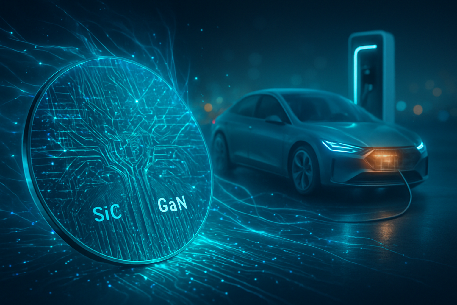
    The global transition to sustainable energy has reached a pivotal tipping point this week as the foundational hardware of the electric vehicle (EV) industry undergoes its most significant transformation in decades. On January 14, 2026, Mitsubishi Electric (OTC: MIELY) announced it would begin shipping samples of its newest trench Silicon Carbide (SiC) MOSFET bare dies on January 21, marking a definitive shift away from traditional silicon-based power electronics. This development is not merely a marginal improvement; it represents a fundamental re-engineering of how energy is managed, moving the industry toward "wide-bandgap" (WBG) materials that promise to unlock unprecedented range for EVs and near-instantaneous charging speeds.

    As of early 2026, the era of "Good Enough" silicon is officially over for high-performance applications. The rapid deployment of Gallium Nitride (GaN) and Silicon Carbide (SiC) in everything from 800V vehicle architectures to 500kW ultra-fast chargers is slashing energy waste and enabling a leaner, more efficient "green" grid. With Mitsubishi’s latest shipment of 750V and 1200V trench-gate dies, the industry is witnessing a "50-70-90" shift: a 50% reduction in power loss compared to previous-gen SiC, a 70% reduction compared to traditional silicon, and a push toward 99% total system efficiency in power conversion.

    The Trench Revolution: Technical Leaps in Power Density

    The technical core of this transition lies in the move from "Planar" to "Trench" architectures in SiC MOSFETs. Mitsubishi Electric's new bare dies, including the 750V WF0020P-0750AA series, utilize a proprietary trench structure where gate electrodes are etched vertically into the wafer. This design drastically increases cell density and reduces "on-resistance," the primary culprit behind heat generation and energy loss. Unlike traditional Silicon Insulated-Gate Bipolar Transistors (Si-IGBTs), which have dominated the industry for 30 years, these SiC devices can handle significantly higher voltages and temperatures while maintaining a footprint that is nearly 60% smaller.

    Beyond SiC, Gallium Nitride (GaN) has made its own breakthrough into the 800V EV domain. Historically relegated to consumer electronics and low-power chargers, new "Vertical GaN" architectures launched in late 2025 now allow GaN to operate at 1200V+ levels. While SiC remains the "muscle" for the main traction inverters that drive a car's wheels, GaN has become the "speedster" for onboard chargers (OBC) and DC-DC converters. Because GaN can switch at frequencies in the megahertz range—orders of magnitude faster than silicon—it allows for much smaller passive components, such as transformers and inductors. This "miniaturization" has led to a 40% reduction in the weight of power electronics in 2026 model-year vehicles, directly translating to more miles per kilowatt-hour.

    Initial reactions from the power electronics community have been overwhelmingly positive. Dr. Elena Vance, a senior semiconductor analyst, noted that "the efficiency gains we are seeing with the 2026 trench-gate chips are the equivalent of adding 30-40 miles of range to an EV without increasing the battery size." Furthermore, the use of "Oblique Ion Implantation" in Mitsubishi's process has solved the long-standing trade-off between power loss and short-circuit robustness, a technical hurdle that had previously slowed the adoption of SiC in the most demanding automotive environments.

    A New Hierarchy: Market Leaders and the 300mm Race

    The shift to WBG materials has completely redrawn the competitive map of the semiconductor industry. STMicroelectronics (NYSE: STM) has solidified its lead as the dominant SiC supplier, capturing nearly 45% of the automotive market through its massive vertically integrated production hub in Catania, Italy. However, the most disruptive market move of 2026 came from Infineon Technologies (OTC: IFNNY), which recently operationalized the world’s first 300mm (12-inch) power GaN production line. This allows for a 2.3x higher chip yield per wafer, effectively commoditizing high-efficiency power chips that were once considered luxury components.

    The landscape also features a reborn Wolfspeed (NYSE: WOLF), which emerged from a 2025 restructuring as a "pure-play" SiC powerhouse. Operating the world’s largest fully automated 200mm fab in New York, Wolfspeed is now focusing on the high-end 1200V+ market required for heavy-duty trucking and AI data centers. Meanwhile, specialized players like Navitas Semiconductor (NASDAQ: NVTS) are dominating the "GaNFast" integrated circuit market, pushing the efficiency of 500kW fast chargers to the "Golden 99%" mark. This level of efficiency is critical because it eliminates the need for massive, expensive liquid cooling systems in chargers, allowing for slimmer, more reliable "plug-and-go" infrastructure.

    Strategic partnerships are also shifting. Automakers like Tesla (NASDAQ: TSLA) and BYD (OTC: BYDDF) are increasingly moving away from buying discrete components and are instead co-developing custom "power modules" with companies like onsemi (NASDAQ: ON). This vertical integration allows OEMs to optimize the thermal management of the SiC/GaN chips specifically for their unique chassis designs, further widening the gap between legacy manufacturers and the new "software-and-silicon" defined car companies.

    AI and the Grid: The Brains Behind the Power

    The "Green Energy Transition" is no longer just about better materials; it is increasingly about the intelligence controlling them. In 2026, the integration of Edge AI into power modules has become the standard. Mitsubishi's 1700V modules now feature Real-Time Control (RTC) circuits that use machine learning algorithms to predict and prevent short-circuits within nanoseconds. This "Smart Power" approach allows the system to push the SiC chips to their physical limits while maintaining a safety buffer that was previously impossible.

    This development fits into a broader trend where AI optimizes the entire energy lifecycle. In the 500kW fast chargers appearing at highway hubs this year, AI-driven switching optimization dynamically adjusts the frequency of the GaN/SiC switches based on the vehicle's state-of-charge and the grid's current load. This reduces "switching stress" and extends the lifespan of the charger by up to 30%. Furthermore, Deep Learning is now used in the manufacturing of these chips themselves; companies like Applied Materials use AI to scan SiC crystals for microscopic "killer defects," bringing the yield of high-voltage wafers closer to that of traditional silicon and lowering the cost for the end consumer.

    The wider significance of this shift cannot be overstated. By reducing the heat loss in power conversion, the world is effectively "saving" terawatts of energy that would have otherwise been wasted as heat. In an era where AI data centers are putting unprecedented strain on the electrical grid, the efficiency gains provided by SiC and GaN are becoming a critical pillar of global energy security, ensuring that the transition to EVs does not collapse the existing power infrastructure.

    Looking Ahead: The Road to 1.2MW and Beyond

    As we move deeper into 2026, the next frontier for WBG materials is the Megawatt Charging System (MCS) for commercial shipping and aviation. Experts predict that the 1700V and 3300V SiC MOSFETs currently being sampled by Mitsubishi and its peers will be the backbone of 1.2MW charging stations, capable of refilling a long-haul electric semi-truck in under 20 minutes. These high-voltage systems will require even more advanced "SBD-embedded" MOSFETs, which integrate Schottky Barrier Diodes directly into the chip to maximize power density.

    On the horizon, the industry is already looking toward "Gallium Oxide" (Ga2O3) as a potential successor to SiC in the 2030s, offering even wider bandgaps for ultra-high-voltage applications. However, for the next five years, the focus will remain on the maturation of the GaN-on-Silicon and SiC-on-SiC ecosystems. The primary challenge remains the supply chain of raw materials, particularly the high-purity carbon and silicon required for SiC crystal growth, leading many nations to designate these semiconductors as "critical strategic assets."

    A New Standard for a Greener Future

    The shipment of Mitsubishi Electric’s latest SiC samples this week is more than a corporate milestone; it is a signpost for the end of the Silicon Age in power electronics. The transition to GaN and SiC has enabled a 70% reduction in power losses, a 5-7% increase in EV range, and the birth of 500kW fast-charging networks that finally rival the convenience of gasoline.

    As we look toward the remainder of 2026, the key developments to watch will be the scaling of 300mm GaN production and the integration of these high-efficiency chips into the "smart grid." The significance of this breakthrough in technology history will likely be compared to the transition from vacuum tubes to transistors—a fundamental shift that makes the "impossible" (like a 600-mile range EV that charges in 10 minutes) a standard reality. The green energy transition is now being fueled by the smallest of switches, and they are faster, cooler, and more efficient than ever before.


    This content is intended for informational purposes only and represents analysis of current technology and market developments.

    TokenRing AI delivers enterprise-grade solutions for multi-agent AI workflow orchestration, AI-powered development tools, and seamless remote collaboration platforms.
    For more information, visit https://www.tokenring.ai/.
  • The 1,000,000-Watt Rack: Mitsubishi Electric Breakthrough in Trench SiC MOSFETs Solves AI’s Power Paradox

    The 1,000,000-Watt Rack: Mitsubishi Electric Breakthrough in Trench SiC MOSFETs Solves AI’s Power Paradox

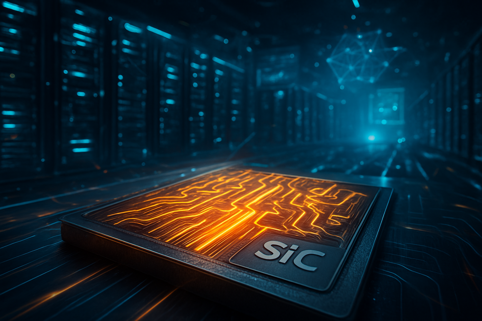
    In a move that signals a paradigm shift for high-density computing and sustainable transport, Mitsubishi Electric Corp (TYO: 6503) has announced a major breakthrough in Wide-Bandgap (WBG) power semiconductors. On January 14, 2026, the company revealed it would begin sample shipments of its next-generation trench Silicon Carbide (SiC) MOSFET bare dies on January 21. These chips, which utilize a revolutionary "trench" architecture, represent a 50% reduction in power loss compared to traditional planar SiC devices, effectively removing one of the primary thermal bottlenecks currently capping the growth of artificial intelligence and electric vehicle performance.

    The announcement comes at a critical juncture as the technology industry grapples with the energy-hungry nature of generative AI. With the latest AI-accelerated server racks now demanding up to 1 megawatt (1MW) of power, traditional silicon-based power conversion has hit a physical "efficiency wall." Mitsubishi Electric's new trench SiC technology is designed to operate in these extreme high-density environments, offering superior heat resistance and efficiency that allows power modules to shrink in size while handling significantly higher voltages. This development is expected to accelerate the deployment of next-generation data centers and extend the range of electric vehicles (EVs) by as much as 7% through more efficient traction inverters.

    Technical Superiority: The Trench Architecture Revolution

    At the heart of Mitsubishi Electric’s breakthrough is the transition from a "planar" gate structure to a "trench" design. In a traditional planar MOSFET, electricity flows horizontally across the surface of the chip before moving vertically, a path that inherently creates higher resistance and limits chip density. Mitsubishi’s new trench SiC-MOSFETs utilize a proprietary "oblique ion implantation" method. By implanting nitrogen in a specific diagonal orientation, the company has created a high-concentration layer that allows electricity to flow more easily through vertical channels. This innovation has resulted in a world-leading specific ON-resistance of approximately 1.84 mΩ·cm², a metric that translates directly into lower heat generation and higher efficiency.

    Technical specifications for the initial four models (WF0020P-0750AA through WF0080P-0750AA) indicate a rated voltage of 750V with ON-resistance ranging from 20 mΩ to 80 mΩ. Beyond mere efficiency, Mitsubishi has solved the "reliability gap" that has long plagued trench SiC devices. Trench structures are notorious for concentrated electric fields at the bottom of the "V" or "U" shape, which can degrade the gate-insulating film over time. To counter this, Mitsubishi engineers developed a unique electric-field-limiting structure by vertically implanting aluminum at the bottom of the trench. This protective layer reduces field stress to levels comparable to older planar devices, ensuring a stable lifecycle even under the high-speed switching demands of AI power supply units (PSUs).

    The industry reaction has been overwhelmingly positive, with power electronics researchers noting that Mitsubishi's focus on bare dies is a strategic masterstroke. By providing the raw chips rather than finished modules, Mitsubishi is allowing companies like NVIDIA Corp (NASDAQ: NVDA) and high-end EV manufacturers to integrate these power-dense components directly into custom liquid-cooled power shelves. Experts suggest that the 50% reduction in switching losses will be the deciding factor for engineers designing the 12kW+ power supplies required for the latest "Rubin" class GPUs, where every milliwatt saved reduces the massive cooling overhead of 1MW data center racks.

    Market Warfare: The Race for 200mm Dominance

    The release of these trench MOSFETs places Mitsubishi Electric in direct competition with a field of energized rivals. STMicroelectronics (NYSE: STM) currently holds the largest market share in the SiC space and is rapidly scaling its own 200mm (8-inch) wafer production in Italy and China. Similarly, Infineon Technologies AG (OTC: IFNNY) has recently brought its massive Kulim, Malaysia fab online, focusing on "CoolSiC" Gen2 trench devices. However, Mitsubishi’s proprietary gate oxide stability and its "bare die first" delivery strategy for early 2026 may give it a temporary edge in the high-performance "boutique" sector of the market, specifically for 800V EV architectures.

    The competitive landscape is also seeing a resurgence from Wolfspeed, Inc. (NYSE: WOLF), which recently emerged from a major restructuring to focus exclusively on its Mohawk Valley 8-inch fab. Meanwhile, ROHM Co., Ltd. (TYO: 6963) has been aggressive in the Japanese and Chinese markets with its 5th-generation trench designs. Mitsubishi’s entry into mass-production sample shipments marks a "normalization" of the 200mm SiC era, where increased yields are finally beginning to lower the "SiC tax"—the premium price that has historically kept Wide-Bandgap materials out of mid-range consumer electronics.

    Strategically, Mitsubishi is positioning itself as the go-to partner for the Open Compute Project (OCP) standards. As hyperscalers like Google and Meta move toward 1MW racks, they are shifting from 48V DC power distribution to high-voltage DC (HVDC) systems of 400V or 800V. Mitsubishi’s 750V-rated trench dies are perfectly positioned for the DC-to-DC conversion stages in these environments. By drastically reducing the footprint of the power infrastructure—sometimes by as much as 75% compared to silicon—Mitsubishi is enabling data center operators to pack more compute into the same physical square footage, a move that is essential for the survival of the current AI boom.

    Beyond the Chips: Solving the AI Sustainability Crisis

    The broader significance of this breakthrough cannot be overstated: it is a direct response to the "AI Power Crisis." The current generation of AI hardware, such as the Advanced Micro Devices, Inc. (NASDAQ: AMD) Instinct MI355X and NVIDIA’s Blackwell systems, has pushed the power density of data centers to a breaking point. A single AI rack in 2026 can consume as much electricity as a small town. Without the efficiency gains provided by Wide-Bandgap materials like SiC, the thermal load would require cooling systems so massive they would negate the economic benefits of the AI models themselves.

    This milestone is being compared to the transition from vacuum tubes to transistors in the mid-20th century. Just as the transistor allowed for the miniaturization of computers, SiC is allowing for the "miniaturization of power." By achieving 98% efficiency in power conversion, Mitsubishi's technology ensures that less energy is wasted as heat. This has profound implications for global sustainability goals; even a 1% increase in efficiency across the global data center fleet could save billions of kilowatt-hours annually.

    However, the rapid shift to SiC is not without concerns. The industry remains wary of supply chain bottlenecks, as the raw material—silicon carbide boules—is significantly harder to grow than standard silicon. Furthermore, the high-speed switching of SiC can create electromagnetic interference (EMI) issues in sensitive AI server environments. Mitsubishi’s unique gate oxide manufacturing process aims to address some of these reliability concerns, but the integration of these high-frequency components into existing legacy infrastructure remains a challenge for the broader engineering community.

    The Horizon: 2kV Chips and the End of Silicon

    Looking toward the late 2020s, the roadmap for trench SiC technology points toward even higher voltages and more extreme integration. Experts predict that Mitsubishi and its competitors will soon debut 2kV and 3.3kV trench MOSFETs, which would revolutionize the electrical grid itself. These devices could lead to "Solid State Transformers" that are a fraction of the size of current neighborhood transformers, enabling a more resilient and efficient smart grid capable of handling the intermittent nature of renewable energy sources like wind and solar.

    In the near term, we can expect to see these trench dies appearing in "Fusion" power modules that combine the best of Silicon and Silicon Carbide to balance cost and performance. Within the next 12 to 18 months, the first consumer EVs featuring these Mitsubishi trench dies are expected to hit the road, likely starting with high-end performance models that require the 20mΩ ultra-low resistance for maximum acceleration and fast-charging capabilities. The challenge for Mitsubishi will be scaling production fast enough to meet the insatiable demand of the "Mag-7" tech giants, who are currently buying every high-efficiency power component they can find.

    The industry is also watching for the potential "GaN-on-SiC" (Gallium Nitride on Silicon Carbide) hybrid chips. While SiC dominates the high-voltage EV and data center market, GaN is making inroads in lower-voltage consumer applications. The ultimate "holy grail" for power electronics would be a unified architecture that utilizes Mitsubishi's trench SiC for the main power stage and GaN for the ultra-high-frequency control stages, a development that researchers believe is only a few years away.

    A New Era for High-Power AI

    In summary, Mitsubishi Electric's announcement of trench SiC-MOSFET sample shipments marks a definitive end to the "Planar Era" of power semiconductors. By achieving a 50% reduction in power loss and solving the thermal reliability issues of trench designs, Mitsubishi has provided the industry with a vital tool to manage the escalating power demands of the AI revolution and the transition to 800V electric vehicle fleets. These chips are not just incremental improvements; they are the enabling hardware for the 1MW data center rack.

    As we move through 2026, the significance of this development will be felt across the entire tech ecosystem. For AI companies, it means more compute per watt. For EV owners, it means faster charging and longer range. And for the planet, it represents a necessary step toward decoupling technological progress from exponential energy waste. Watch for the results of the initial sample evaluations in the coming months; if the 20mΩ dies perform as advertised in real-world "Rubin" GPU clusters, Mitsubishi Electric may find itself at the center of the next great hardware gold rush.


    This content is intended for informational purposes only and represents analysis of current AI developments.

    TokenRing AI delivers enterprise-grade solutions for multi-agent AI workflow orchestration, AI-powered development tools, and seamless remote collaboration platforms.
    For more information, visit https://www.tokenring.ai/.

    Published on January 16, 2026.