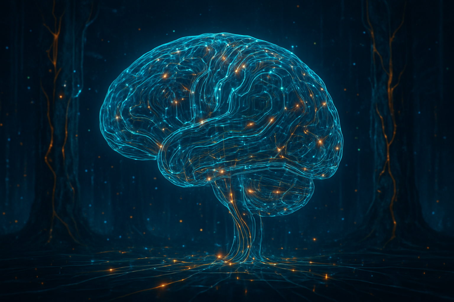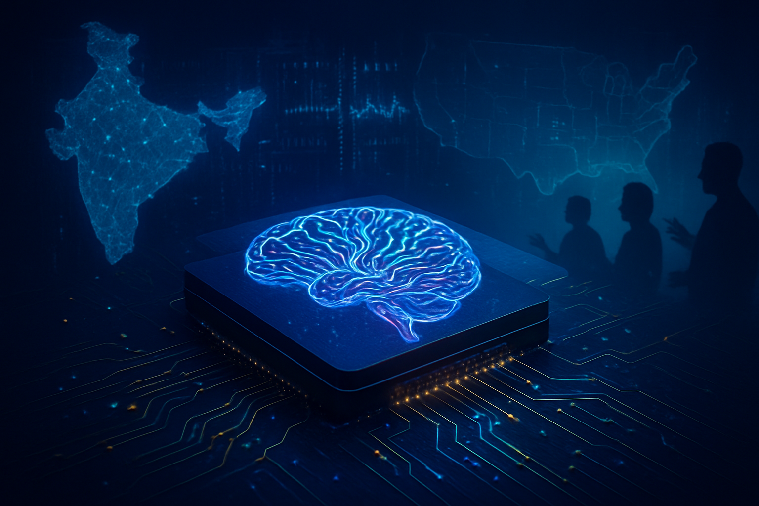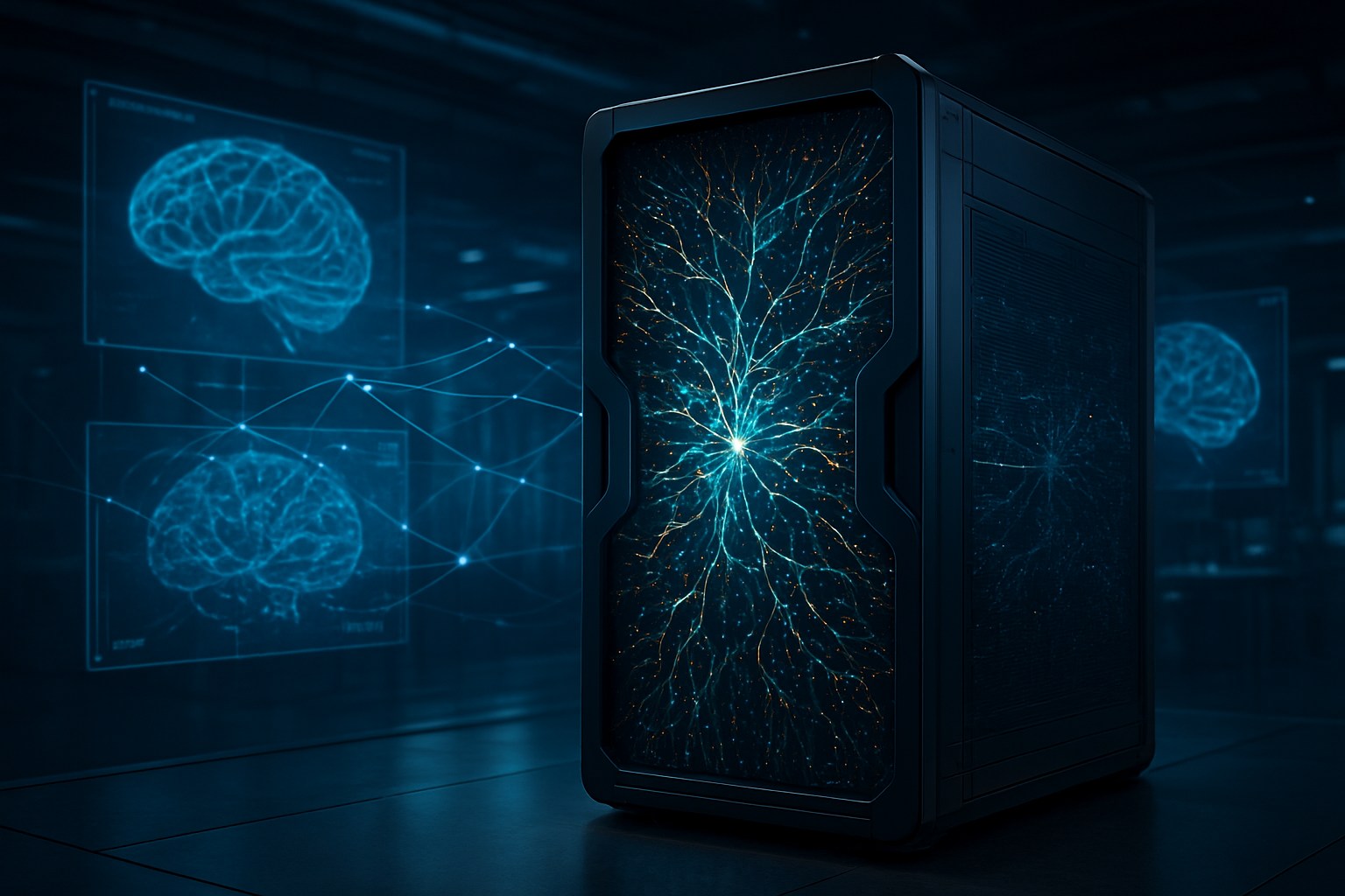
The era of brute-force artificial intelligence is facing a reckoning. As the power demands of traditional data centers soar to unsustainable levels, Intel Corporation (NASDAQ: INTC) has unveiled a radical alternative that mimics the most efficient computer known to exist: the human brain. Hala Point, the world’s largest neuromorphic system, marks a definitive shift from the "muscle" of traditional computing to the "intelligence" of biological architecture. Deployed at Sandia National Laboratories, this 1.15-billion-neuron system is not just a research project; it is a direct challenge to the energy-intensive status quo of modern AI development.
By utilizing the specialized Loihi 2 processor, Hala Point achieves a staggering 100x better energy efficiency than traditional GPUs for event-driven AI workloads. Unlike the synchronous, data-heavy processing required by today’s Large Language Models (LLMs), Hala Point operates on a principle of sparsity and "spikes," where artificial neurons only consume energy when they have information to process. This milestone arrives at a critical juncture as the industry grapples with the "energy wall"—the point at which the electrical and cooling costs of training massive models begin to outweigh their commercial utility.
Architecting the Synthetic Mind: Inside Loihi 2 and the Hala Point Chassis
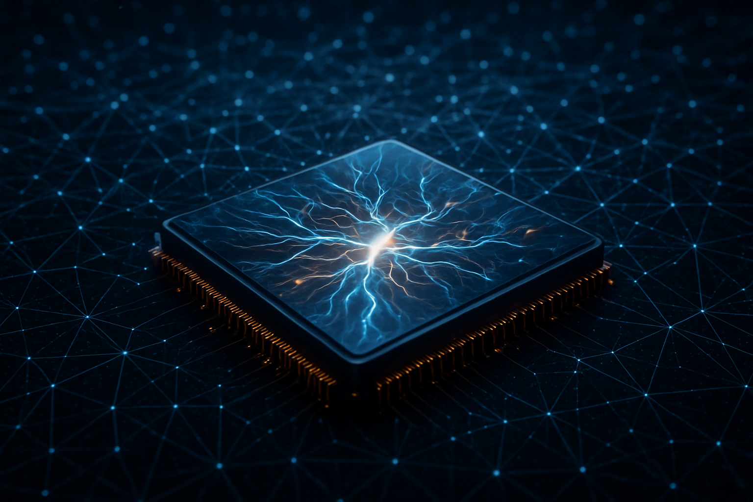
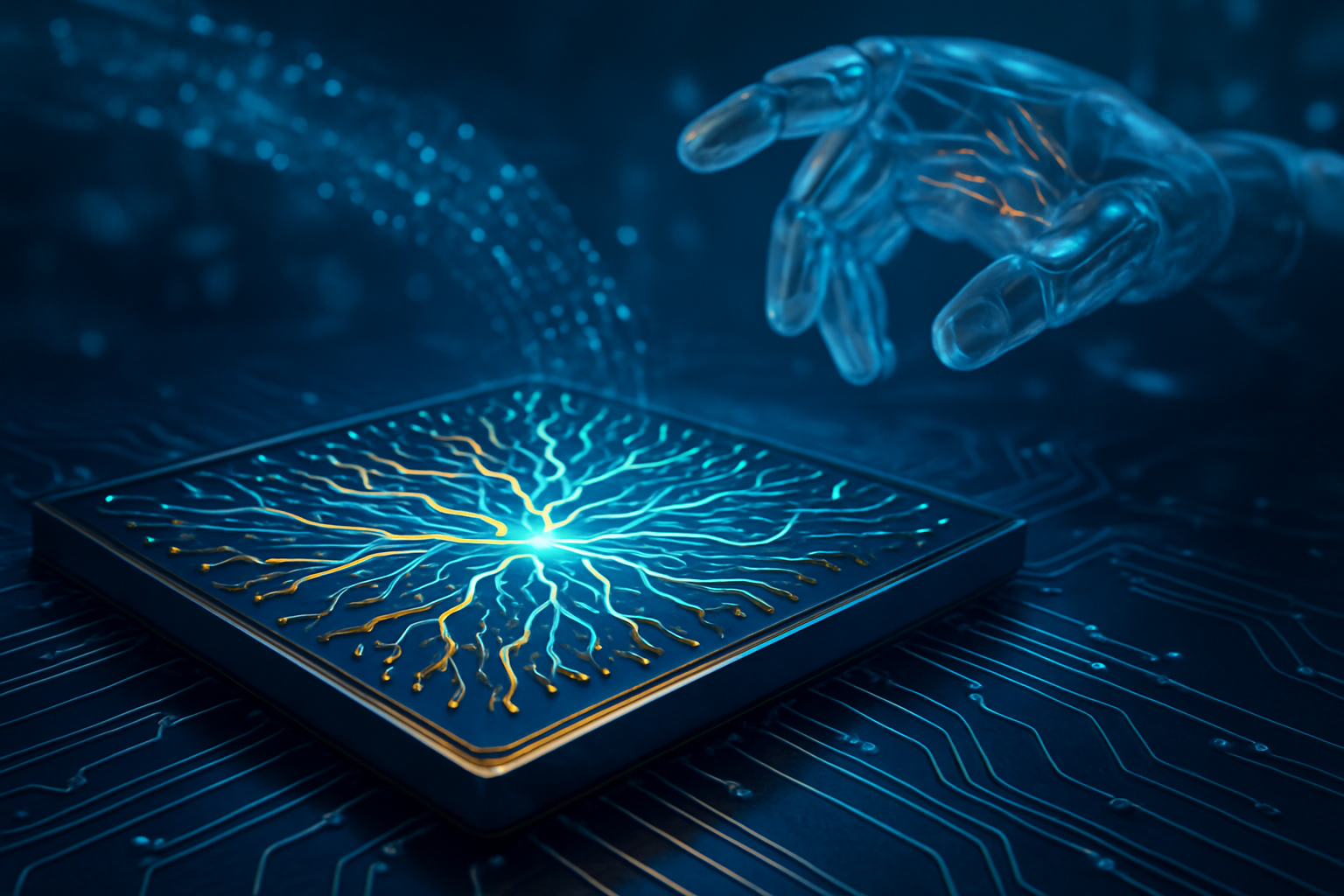
At the heart of Hala Point lies a massive array of 1,152 Loihi 2 neuromorphic research processors. Manufactured on the advanced Intel 4 process node, this system packs 1.15 billion artificial neurons and 128 billion synapses into a six-rack-unit chassis roughly the size of a microwave oven. This represents a nearly 25-fold increase in capacity over Intel’s previous-generation system, Pohoiki Springs. The architecture is fundamentally "non-von Neumann," meaning it eliminates the constant shuffling of data between a central processor and separate memory—a process that accounts for the vast majority of energy waste in traditional silicon.
Technically, Hala Point is designed for "event-driven" computing. In a standard GPU, like those produced by NVIDIA (NASDAQ: NVDA), every transistor is essentially "clocked" and active during a computation, regardless of whether the data is changing. In contrast, Hala Point’s neurons "spike" only when triggered by a change in input. This allows for massive parallelism without the massive heat signature. Benchmarks released in late 2025 and early 2026 show that for optimization problems and sparse neural networks, Hala Point can achieve up to 15 trillion 8-bit operations per second per watt (TOPS/W). For comparison, even the most advanced Blackwell-series GPUs from NVIDIA struggle to match a fraction of this efficiency in real-time, non-batched inference scenarios.
The reaction from the research community has been one of cautious optimism followed by rapid adoption in specialized fields. Scientists at Sandia National Laboratories have already begun using Hala Point to solve complex Partial Differential Equations (PDEs)—the mathematical foundations of physics and climate modeling. Through the development of the "NeuroFEM" algorithm, researchers have demonstrated that they can perform exascale-level simulations with a power draw of just 2.6 kilowatts, a feat that would normally require megawatts of power on a traditional supercomputer.
The Efficiency Pivot: Intel’s Strategic Moat Against NVIDIA’s Dominance
The deployment of Hala Point signifies a broader market shift that analysts are calling "The Efficiency Pivot." While NVIDIA has dominated the AI landscape by providing the raw "muscle" needed to train massive transformers, Intel is carving out a "third stream" of computing that focuses on the edge and real-time adaptation. This development poses a long-term strategic threat to the high-margin data center business of both NVIDIA and Advanced Micro Devices (NASDAQ: AMD), particularly as companies look to deploy AI in power-constrained environments like autonomous robotics, satellites, and mobile devices.
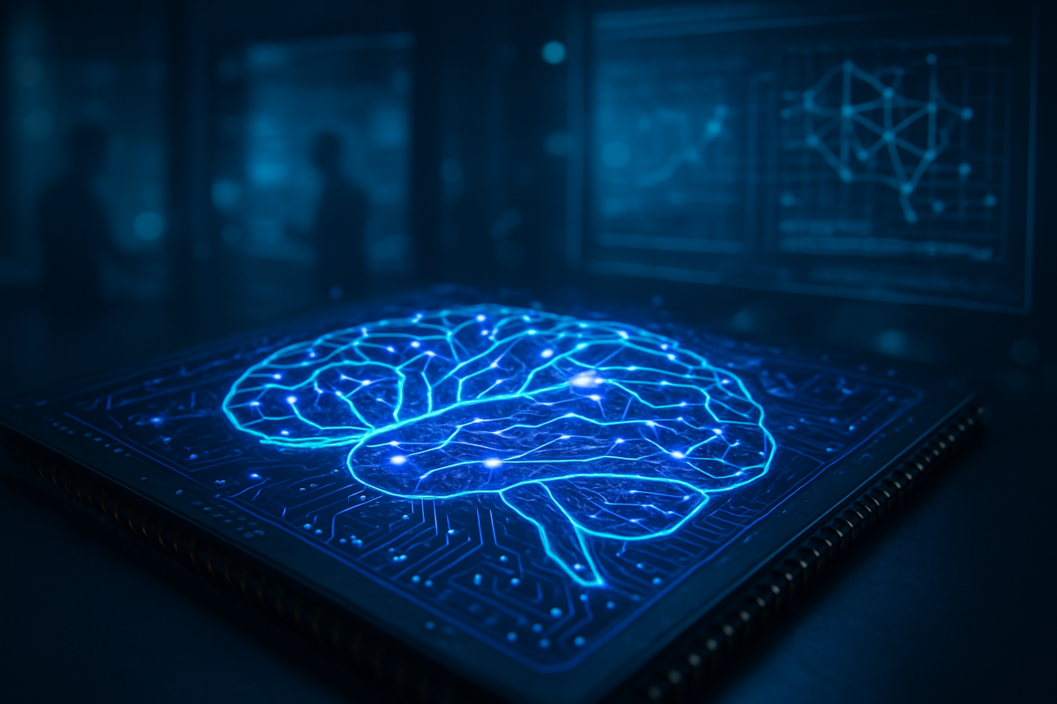
For Intel, Hala Point is a centerpiece of its IDM 2.0 strategy, proving that the company can still lead in architectural innovation even while playing catch-up in the GPU market. By positioning Loihi 2 as the premier solution for "Physical AI"—AI that interacts with the real world in real-time—Intel is targeting a high-growth sector where latency and battery life are more important than batch-processing throughput. This has already led to interest from sectors like telecommunications, where Ericsson has explored using neuromorphic chips to optimize wireless signals in 5G and 6G base stations with minimal energy overhead.
The competitive landscape is further complicated by the arrival of specialized hardware from other tech giants. International Business Machines (NYSE: IBM) has seen success with its NorthPole chip, which uses "spatial computing" to eliminate the memory wall. However, Intel’s Hala Point remains the only system capable of brain-scale spiking neural networks (SNNs), a distinction that keeps it at the forefront of "continuous learning." While a traditional AI model is "frozen" after training, Hala Point’s Loihi 2 cores feature programmable learning engines that allow the system to adapt to new data on the fly without losing its previous knowledge.
Beyond the Transistor: The Societal and Environmental Imperative
The significance of Hala Point extends far beyond a simple benchmark. In the broader AI landscape, there is a growing concern regarding the environmental footprint of the "AI Gold Rush." With data centers projected to consume nearly 3% of global electricity by 2030, the 100x efficiency gain offered by neuromorphic computing is no longer a luxury—it is a necessity. Hala Point serves as a proof of concept that we can achieve "brain-scale" intelligence without building power plants specifically to fuel it.
This shift mirrors previous milestones in computing history, such as the transition from vacuum tubes to transistors or the rise of RISC architecture. However, the move to neuromorphic computing is even more profound because it challenges the very way we think about information. By mimicking the "sparse" nature of biological thought, Hala Point avoids the pitfalls of the "Scaling Laws" that suggest we must simply build bigger and more power-hungry models to achieve smarter AI. Instead, it suggests that intelligence can be found in the efficiency of the connections, not just the number of parameters.
There are, however, potential concerns. The software ecosystem for neuromorphic hardware, such as Intel’s "Lava" framework, is still maturing and lacks the decades of optimization found in NVIDIA’s CUDA. Critics argue that until developers can easily port their existing PyTorch or TensorFlow models to spiking hardware, the technology will remain confined to national laboratories and elite research institutions. Furthermore, the "real-time learning" capability of these systems introduces new questions about AI safety and predictability, as a system that learns continuously may behave differently tomorrow than it does today.
The Road to Loihi 3: Commercializing the Synthetic Brain
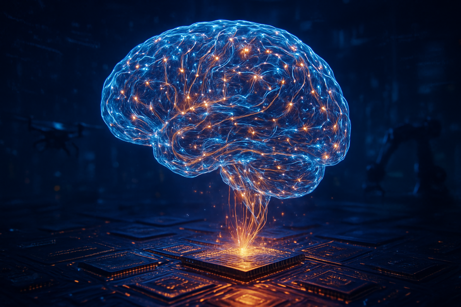
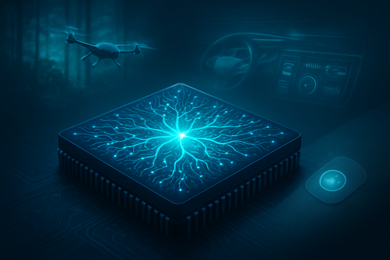
Looking ahead, the roadmap for Intel’s neuromorphic division is ambitious. As of early 2026, industry insiders are already tracking the development of "Loihi 3," which is expected to offer an 8x increase in neuron density and a move toward commercial-grade deployment. While Hala Point is a massive research testbed, the next generation of this technology is likely to be miniaturized for use in consumer products. Imagine a drone that can navigate a dense forest at 80 km/h by "learning" the layout in real-time, or a prosthetic limb that adapts to a user’s movements with the fluid grace of a biological appendage.
Experts predict that the next two years will see the rise of "Hybrid AI" models. In this configuration, traditional GPUs will still handle the heavy lifting of initial training, while neuromorphic chips like Loihi will handle the deployment and "on-device" refinement. This would allow for a smartphone that learns its user's unique speech patterns or health metrics locally, ensuring both extreme privacy and extreme efficiency. The challenge remains the integration of these disparate architectures into a unified software stack that is accessible to the average developer.
In the near term, watch for more results from Sandia National Laboratories as they push Hala Point toward more complex "multi-physics" simulations. These results will serve as the "ground truth" for whether neuromorphic hardware can truly replace traditional supercomputers for scientific discovery. If Sandia can prove that Hala Point can reliably model climate change or nuclear fusion with the power draw of a household appliance, the industrial shift toward neuromorphic architecture will become an unstoppable landslide.
A New Chapter in Artificial Intelligence
Intel’s Hala Point is more than a technical achievement; it is a manifesto for the future of computing. By delivering 1.15 billion neurons at 100x the efficiency of current hardware, Intel has demonstrated that the "energy wall" is not an impassable barrier, but a signpost pointing toward a different path. The deployment at Sandia National Laboratories marks the beginning of an era where AI is defined not by how much power it consumes, but by how much it can achieve with the energy it is given.
As we move further into 2026, the success of Hala Point will be measured by how quickly its innovations trickle down into the commercial sector. The "brain-scale" revolution has begun, and while NVIDIA remains the king of the data center for now, Intel’s investment in the architecture of the future has created a formidable challenge. The coming months will likely see a surge in "Efficiency AI" announcements as the rest of the industry tries to match the benchmarks set by Loihi 2. For now, Hala Point stands as a beacon of what is possible when we stop trying to force computers to think like machines and start teaching them to think like us.
This content is intended for informational purposes only and represents analysis of current AI developments.
TokenRing AI delivers enterprise-grade solutions for multi-agent AI workflow orchestration, AI-powered development tools, and seamless remote collaboration platforms.
For more information, visit https://www.tokenring.ai/.