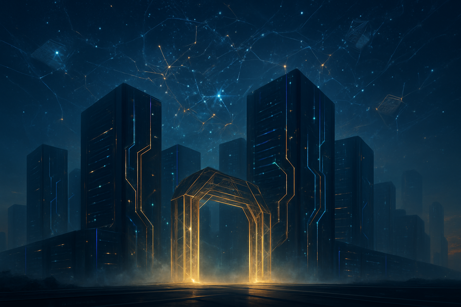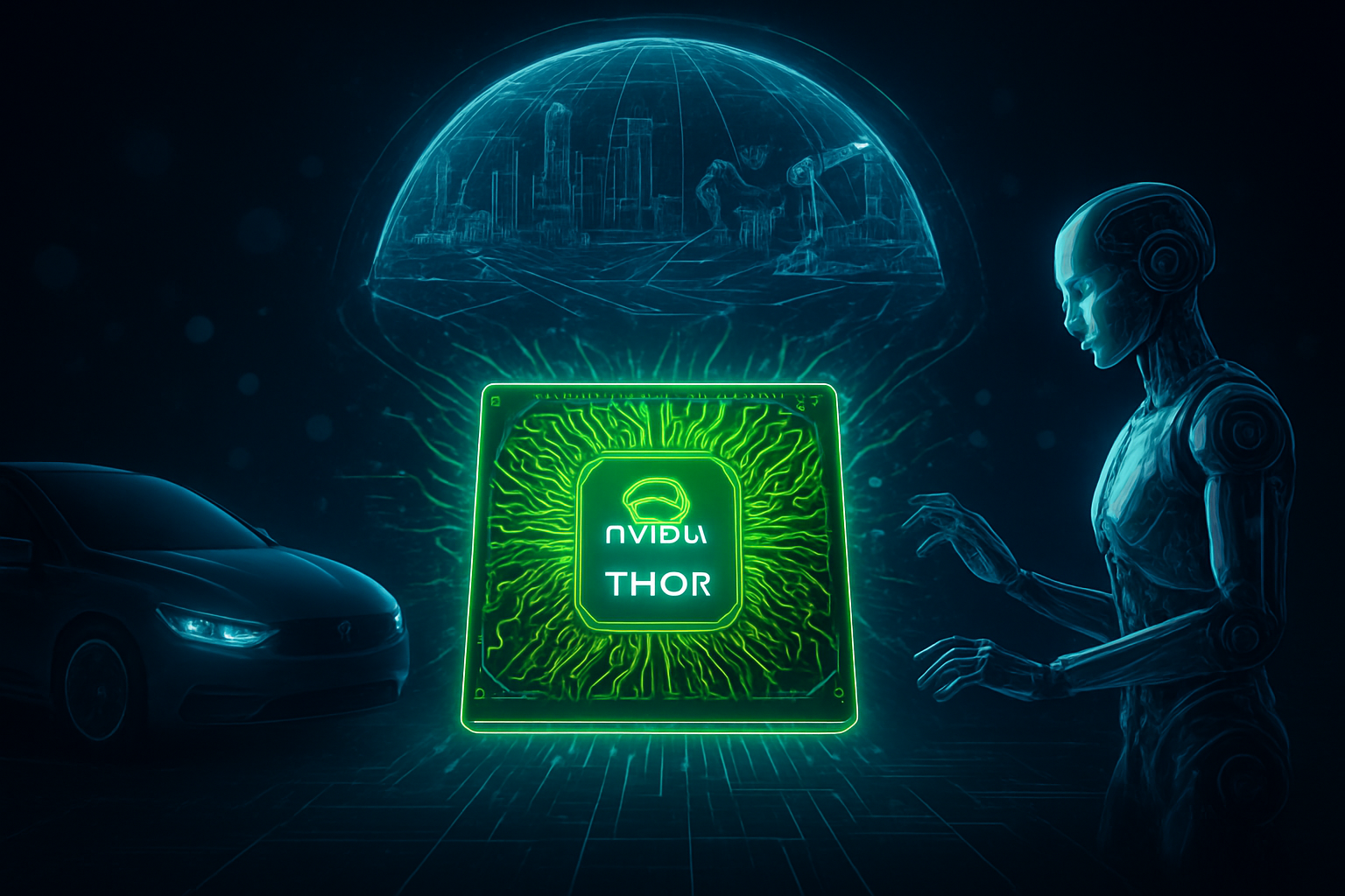
As of February 6, 2026, the boundary between digital simulation and physical reality has effectively dissolved. NVIDIA (NASDAQ: NVDA) has officially moved its DRIVE Thor "superchip" from the development labs into the heart of the global transportation and robotics industries. With the first Thor-powered production vehicles hitting roads in Europe and Asia this quarter, the chip has become more than just a processor; it is the foundational "brain" for a new era of Physical AI.
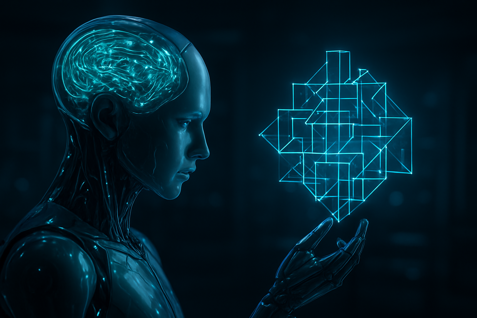
The significance of this milestone cannot be overstated. By centralizing the immense compute requirements of generative AI, autonomous driving, and humanoid movement into a single Blackwell-based architecture, NVIDIA is enabling machines to do more than just follow code—they are now beginning to "understand" the physical world. Through the use of a unified "world model," Thor-equipped machines can predict cause-and-effect relationships in real-time, allowing for a level of safety and autonomy that was once the stuff of science fiction.
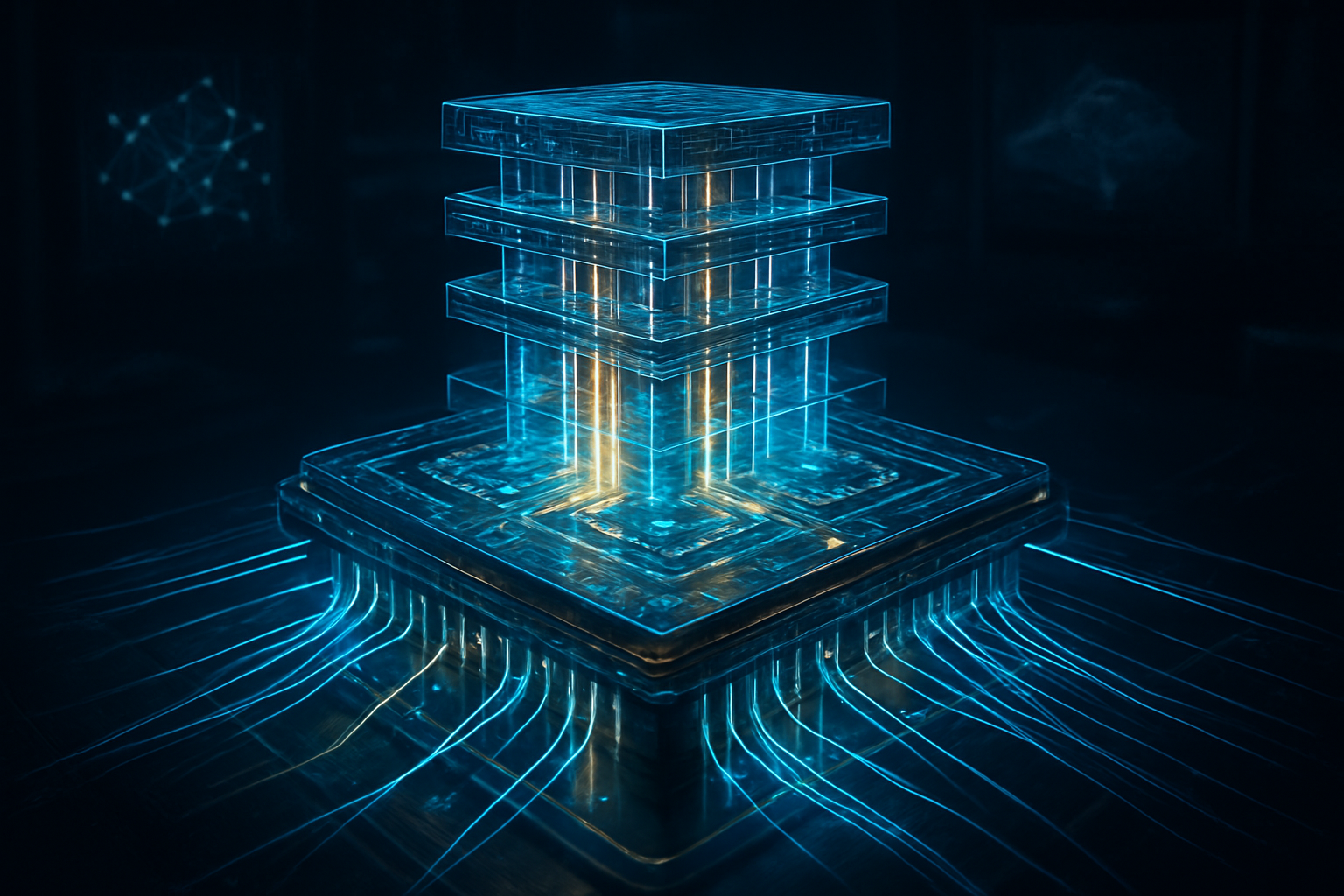
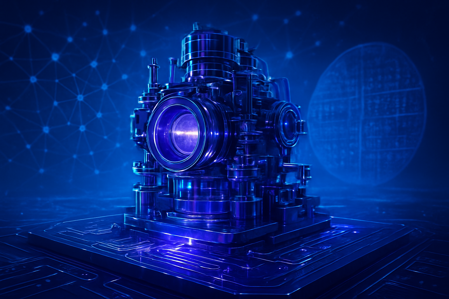
The Technical Core: Blackwell, 2,000 TFLOPS, and the Reasoning Engine
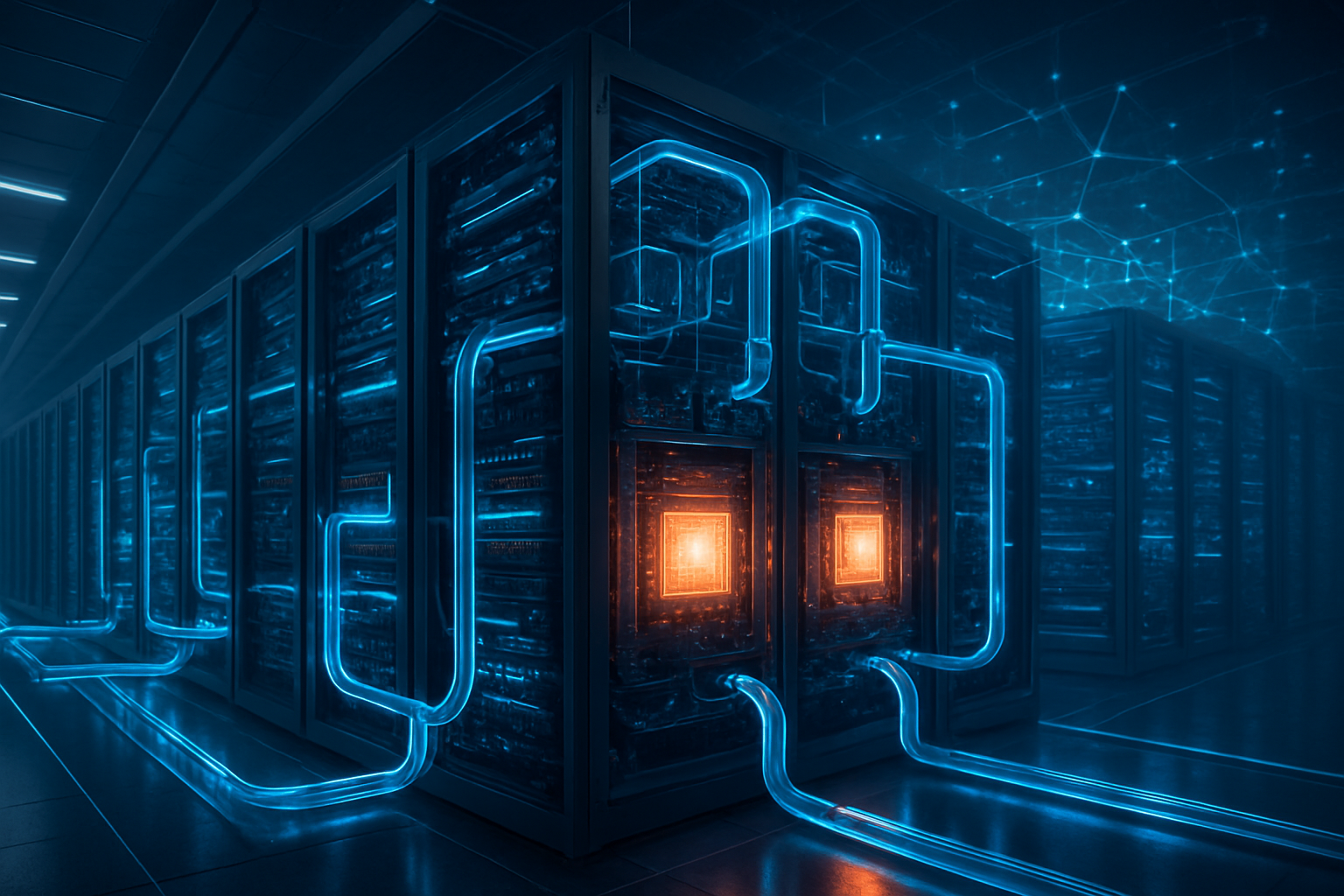
At the heart of the Thor platform lies NVIDIA’s Blackwell architecture, which has been specialized for the high-stakes environment of edge computing. Delivering a staggering 2,000 TFLOPS of 4-bit floating-point (FP4) performance, Thor offers a 7.5x leap over its predecessor, DRIVE Orin. This massive compute overhead is necessary to run the "NVIDIA Cosmos" and "Alpamayo" models—foundation models that act as the machine's cognitive core. Unlike previous generations that relied on fragmented neural networks for perception and planning, Thor uses a unified transformer-based inference engine to process a "world model."
This unified approach allows the chip to simulate thousands of potential future scenarios every second. For instance, the Alpamayo model—a Vision-Language-Action (VLA) model introduced at CES 2026—enables "Chain-of-Thought" reasoning for vehicles. A Thor-powered car no longer just sees a "moving object"; it reasons that "a child chasing a ball is likely to enter the street," and adjusts its path preemptively. This move toward reasoning-based AI marks a departure from the pattern-matching algorithms of the early 2020s, providing a more robust solution for the "long-tail" edge cases that have historically plagued autonomous systems.
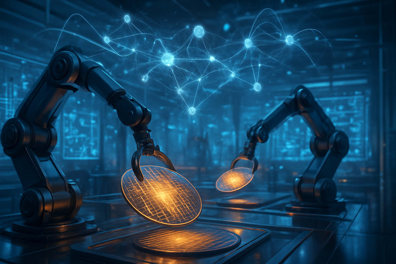
Furthermore, NVIDIA has expanded the platform with "Jetson Thor," a version specifically optimized for humanoid robotics. This module runs the Isaac GR00T N1.6 foundation model, allowing robots to learn complex dexterous manipulations and human-like locomotion. By utilizing Multi-Instance GPU (MIG) technology, Thor can simultaneously manage the complex balance required for a bipedal robot to walk while processing natural language commands and managing high-speed sensor fusion—all on a single, energy-efficient SoC.
Reshaping the Competitive Landscape of Silicon and Robotics
The rollout of Thor has sent shockwaves through the tech industry, solidifying NVIDIA’s position as the primary architect of the physical AI ecosystem. Major automotive giants, including Mercedes-Benz (OTC: MBGYY), Volvo (OTC: VLVLY), and Jaguar Land Rover, have already integrated Thor into their 2026 flagship models. Perhaps more importantly, the aggressive adoption by Chinese EV leaders like BYD (OTC: BYDDF), XPENG (NYSE: XPEV), Li Auto (NASDAQ: LI), and ZEEKR (NYSE: ZK) suggests that Thor has become the de facto standard for high-end intelligent vehicles.
This dominance presents a significant challenge to competitors like Qualcomm (NASDAQ: QCOM) and Tesla (NASDAQ: TSLA). While Tesla continues to iterate on its proprietary FSD hardware, NVIDIA’s open ecosystem—which provides not just the chip but the entire "Full Stack" of simulation tools and foundation models—has attracted a vast array of partners. Startups in the autonomous trucking space, such as Aurora (NASDAQ: AUR) and Waabi, are leveraging Thor to achieve Level 4 autonomy with fewer hardware sensors, significantly lowering the barrier to commercialization.
In the robotics sector, the impact is even more transformative. Companies like Boston Dynamics (owned by Hyundai (KRX: 005380)) and NEURA Robotics are now using Jetson Thor to power their latest humanoid prototypes. By providing a standardized, ultra-high-performance compute platform, NVIDIA is doing for robotics what the smartphone did for mobile software: creating a common hardware layer that allows developers to focus on the "intelligence" rather than the underlying silicon.
The Dawn of Physical AI and the Unified World Model
Beyond the specs and market share, Thor represents a fundamental shift in the AI landscape. We are moving from "Cyber AI"—LLMs that process text and images on servers—to "Physical AI," where the model interacts with and changes the physical world. The concept of a unified world model is central to this. By training on "NVIDIA Cosmos," these machines are essentially learning the laws of physics. They understand gravity, friction, and spatial permanence through massive-scale synthetic data generated in NVIDIA’s Omniverse.
This development mirrors the milestone of the original GPT models, but for the physical realm. Just as GPT-3 proved that scaling parameters could lead to linguistic emergence, Thor is proving that scaling compute at the edge can lead to physical intuition. However, this breakthrough is not without its concerns. The reliance on a centralized world model raises questions about data sovereignty and the "black box" nature of AI reasoning. If a Thor-powered robot or car makes a mistake, the complexity of its 2,000-TFLOPS reasoning engine may make it difficult for human investigators to parse exactly why the error occurred.
Comparisons are already being drawn to the introduction of the first iPhone or the launch of the internet. We are witnessing the birth of an "Internet of Moving Things," where every machine is capable of autonomous navigation and complex task execution. The social implications—from the displacement of manual labor to the restructuring of urban infrastructure—are only just beginning to be felt as these machines proliferate in 2026.
Looking Ahead: The Road to 2027 and Beyond
In the near term, we can expect NVIDIA to continue refining the Thor family, likely branching into specialized versions for aviation (eVTOLs) and maritime autonomy. The next major hurdle is the integration of even more sophisticated Vision-Language-Action models that allow robots to operate in unstructured environments, like a busy construction site or a dynamic hospital floor, without any prior mapping. Experts predict that by 2027, "Zero-Shot" robotics—where a robot can perform a task it has never seen before based solely on verbal instructions—will become the new standard, powered by Thor’s successors.
Challenges remain, particularly in the realm of power consumption and thermal management. While Thor is highly efficient for its class, the energy required to run a full world model at 2,000 TFLOPS is significant. We are likely to see a surge in innovation around "neuromorphic" co-processors or even more advanced cooling systems for humanoid robots. Furthermore, as regulators in the EU and the US finalize the 2026 AI Safety Accords, NVIDIA’s ability to provide "explainable AI" through Thor’s reasoning logs will be a critical factor in its continued dominance.
Final Assessment: A Historical Turning Point
NVIDIA’s Thor is more than a successful product launch; it is the catalyst for the "Physical AI" revolution. By providing the massive compute needed to run unified world models at the edge, NVIDIA has effectively given machines a sense of their surroundings and the ability to reason through complex physical interactions. The transition of this technology from experimental silicon to production vehicles and humanoid workers in February 2026 marks a historical turning point in human-machine interaction.
As we move forward into 2026, the key metric for AI success will no longer be how well a model can write an essay, but how safely and efficiently it can navigate a city street or assist in a manufacturing plant. With the Thor ecosystem now firmly established, the tech world is watching closely to see how the competition responds and how society adapts to a world where the objects around us are finally starting to "think."
This content is intended for informational purposes only and represents analysis of current AI developments.
TokenRing AI delivers enterprise-grade solutions for multi-agent AI workflow orchestration, AI-powered development tools, and seamless remote collaboration platforms.
For more information, visit https://www.tokenring.ai/.