Tag: Nvidia Blackwell

  • Silicon Sovereignty: US Levies 25% Section 232 Tariffs on Advanced AI Silicon

    Silicon Sovereignty: US Levies 25% Section 232 Tariffs on Advanced AI Silicon

    In a move that fundamentally reshapes the global semiconductor landscape, the United States government has officially implemented a 25% ad valorem tariff on high-performance AI and computing chips under Section 232 of the Trade Expansion Act of 1962. Formalized via a Presidential Proclamation on January 14, 2026, the tariffs specifically target high-end accelerators that form the backbone of modern large language model (LLM) training and inference. The policy, which went into effect at 12:01 a.m. EST on January 15, marks the beginning of an aggressive "tariffs-for-investment" strategy designed to force the relocation of advanced manufacturing to American soil.

    The immediate significance of this announcement cannot be overstated. By leveraging national security justifications—the hallmark of Section 232—the administration is effectively placing a premium on advanced silicon that is manufactured outside of the United States. While the measure covers a broad range of high-performance logic circuits, it explicitly identifies industry workhorses like NVIDIA’s H200 and AMD’s Instinct MI325X as primary targets. This shift signals a transition from "efficiency-first" global supply chains to a "security-first" domestic mandate, creating a bifurcated market for the world's most valuable technology.

    High-Performance Hardware in the Crosshairs

    The technical scope of the new tariffs is defined by rigorous performance benchmarks rather than just brand names. According to the Proclamation’s Annex, the 25% duty applies to integrated circuits with a Total Processing Performance (TPP) between 14,000 and 21,100, combined with DRAM bandwidth exceeding 4,500 GB/s. This technical net specifically ensnares the NVIDIA (NASDAQ: NVDA) H200, which features 141GB of HBM3E memory, and the AMD (NASDAQ: AMD) Instinct MI325X, a high-capacity 256GB HBM3E powerhouse. These specifications are essential for the massive throughput required by the Blackwell architecture and AMD’s latest enterprise offerings.

    This policy differs from previous export controls by focusing on the import of finished silicon into the U.S., rather than just restricting sales to foreign adversaries. It essentially creates a financial barrier that penalizes domestic reliance on foreign fabrication plants (fabs). Initial reactions from the AI research community have been a mix of strategic concern and cautious optimism. While some researchers fear the short-term cost of compute will rise, industry experts note that the technical specifications are carefully calibrated to capture the current "sweet spot" of enterprise AI, ensuring the government has maximum leverage over the most critical components of the AI revolution.

    Market Disruptions and the "Startup Shield"

    The market implications for tech giants and emerging startups are vastly different due to a sophisticated system of "end-use focused" exemptions. Major hyperscalers such as Microsoft (NASDAQ: MSFT), Alphabet (NASDAQ: GOOGL), and Meta (NASDAQ: META) are largely shielded from the immediate 25% price hike, provided the chips are destined for U.S.-based data centers. This carve-out ensures that the ongoing build-out of the "AI Factory" infrastructure—currently dominated by NVIDIA’s Blackwell (B200/GB200) systems—remains economically viable within American borders.

    Furthermore, the administration has introduced a "Startup Shield," exempting domestic AI developers and R&D labs from the tariffs. This strategic move is intended to maintain the competitive advantage of the U.S. innovation ecosystem while the manufacturing base catches up. However, companies that import these chips for secondary testing or re-export purposes without a domestic end-use certification will face the full 25% levy. This creates a powerful incentive for firms like NVIDIA and AMD to prioritize U.S. customers and domestic supply chain partners, potentially disrupting long-standing distribution channels in Asia and Europe.

    Geopolitical Realignment and the Taiwan Agreement

    This tariff rollout is the "Phase 1" of a broader geopolitical strategy to reshore 2nm and 3nm manufacturing. Coinciding with the tariff announcement, the U.S. and Taiwan signed a landmark $250 billion investment agreement. Under this deal, Taiwanese firms like TSMC (NYSE: TSM) have committed to massive new capacity in states like Arizona. In exchange, these companies receive "preferential Section 232 treatment," allowing them to import advanced chips duty-free at a ratio tied to their U.S. investment milestones. This effectively turns the tariff into a tool for industrial policy, rewarding companies that move their most advanced "crown jewel" fabrication processes to the U.S.

    The move fits into a broader trend of "computational nationalism," where the ability to produce and control AI silicon is viewed as a prerequisite for national sovereignty. It mirrors historical milestones like the 1980s semiconductor trade disputes but on a far more accelerated and high-stakes scale. By targeting the H200 and MI325X—chips that are currently "sold out" through much of 2026—the U.S. is leveraging high demand to force a permanent shift in where the next generation of silicon, such as NVIDIA's Rubin or AMD's MI455X, will be born.

    The Horizon: Rubin, MI455X, and the 2nm Era

    Looking ahead, the industry is already preparing for the "post-Blackwell" era. At CES 2026, NVIDIA CEO Jensen Huang detailed the Rubin (R100) architecture, which utilizes HBM4 memory and a 3nm process, scheduled for production in late 2026. Similarly, AMD has unveiled the MI455X, a 2nm-node beast with 432GB of HBM4 memory. The new Section 232 tariffs are designed to ensure that by the time these next-generation chips reach volume production, the domestic infrastructure—bolstered by the "Tariff Offset Program"—will be ready to handle a larger share of the manufacturing load.

    Near-term challenges remain, particularly regarding the complexity of end-use certifications and the potential for a "grey market" of non-certified silicon. However, analysts predict that the tariff will accelerate the adoption of "American-made" silicon as a premium tier for government and high-security enterprise contracts. As the U.S. domestic fabrication capacity from Intel (NASDAQ: INTC) and TSMC’s American fabs comes online between 2026 and 2028, the financial pressure of the 25% tariff is expected to transition into a permanent structural advantage for domestically produced AI hardware.

    A Pivot Point in AI History

    The January 2026 Section 232 tariffs represent a definitive pivot point in the history of artificial intelligence. It marks the moment when the U.S. government decided that the strategic risk of a distant supply chain outweighed the benefits of globalized production. By exempting startups and domestic data centers, the policy attempts a delicate "Goldilocks" approach: punishing foreign dependency without stifling the very innovation that the chips are meant to power.

    As we move deeper into 2026, the industry will be watching the "Tariff Offset Program" closely to see how quickly it can spur actual domestic output. The success of this measure will be measured not by the revenue the tariffs collect, but by the number of advanced fabs that break ground on American soil in the coming months. For NVIDIA, AMD, and the rest of the semiconductor world, the message is clear: the future of AI is no longer just about who has the fastest chip, but where that chip is made.


    This content is intended for informational purposes only and represents analysis of current AI developments.

    TokenRing AI delivers enterprise-grade solutions for multi-agent AI workflow orchestration, AI-powered development tools, and seamless remote collaboration platforms.
    For more information, visit https://www.tokenring.ai/.

  • Meta Unveils ‘Meta Compute’: A Gigawatt-Scale Blueprint for the Era of Superintelligence

    Meta Unveils ‘Meta Compute’: A Gigawatt-Scale Blueprint for the Era of Superintelligence

    In a move that signals the dawn of the "industrial AI" era, Meta Platforms (NASDAQ: META) has officially launched its "Meta Compute" initiative, a massive strategic overhaul of its global infrastructure designed to power the next generation of frontier models. Announced on January 12, 2026, by CEO Mark Zuckerberg, the initiative unifies the company’s data center engineering, custom silicon development, and energy procurement under a single organizational umbrella. This shift marks Meta's transition from an AI-first software company to a "sovereign-scale" infrastructure titan, aiming to deploy hundreds of gigawatts of power over the next decade.

    The immediate significance of Meta Compute lies in its sheer physical and financial scale. With an estimated 2026 capital expenditure (CAPEX) set to exceed $100 billion, Meta is moving away from the "reactive" scaling of the past three years. Instead, it is adopting a "proactive factory model" that treats AI compute as a primary industrial output. This infrastructure is not just a support system for the company's social apps; it is the engine for what Zuckerberg describes as "personal superintelligence"—AI systems capable of surpassing human performance in complex cognitive tasks, seamlessly integrated into consumer devices like Meta Glasses.

    The Prometheus Cluster and the Rise of the 'AI Tent'

    At the heart of the Meta Compute initiative is the newly completed "Prometheus" facility in New Albany, Ohio. This site represents a radical departure from traditional data center architecture. To bypass the lengthy 24-month construction cycles of concrete facilities, Meta utilized modular, hurricane-proof "tent-style" structures. This innovative "fast-build" approach allowed Meta to bring 1.02 gigawatts (GW) of IT power online in just seven months. The Prometheus cluster is projected to house a staggering 500,000 GPUs, featuring a mix of NVIDIA (NASDAQ: NVDA) GB300 "Clemente" and GV200 "Catalina" systems, making it one of the most powerful concentrated AI clusters in existence.

    Technically, the Meta Compute infrastructure is built to handle the extreme heat and networking demands of Blackwell-class silicon. Each rack houses 72 GPUs, pushing power density to levels that traditional air cooling can no longer manage. Meta has deployed Air-Assisted Liquid Cooling (AALC) and closed-loop direct-to-chip systems to stabilize these massive workloads. For networking, the initiative relies on a Disaggregated Scheduled Fabric (DSF) powered by Arista Networks (NYSE: ANET) 7808 switches and Broadcom (NASDAQ: AVGO) Jericho 3 and Ramon 3 ASICs, ensuring that data can flow between hundreds of thousands of chips with minimal latency.

    This infrastructure is the direct predecessor to the hardware currently training the upcoming Llama 5 model family. While Llama 4—released in April 2025—was trained on clusters exceeding 100,000 H100 GPUs, Llama 5 is expected to utilize the full weight of the Blackwell-integrated Prometheus site. Initial reactions from the AI research community have been split. While many admire the engineering feat of the "AI Tents," some experts, including those within Meta's own AI research labs (FAIR), have voiced concerns about the "Bitter Lesson" of scaling. Rumors have circulated that Chief Scientist Yann LeCun has shifted focus away from the scaling-law obsession, preferring to explore alternative architectures that might not require gigawatt-scale power to achieve reasoning.

    The Battle of the Gigawatts: Competitive Moats and Energy Wars

    The Meta Compute initiative places Meta in direct competition with the most ambitious infrastructure projects in history. Microsoft (NASDAQ: MSFT) and OpenAI are currently developing "Stargate," a $500 billion consortium project aimed at five major sites across the U.S. with a long-term goal of 10 GW. Meanwhile, Amazon (NASDAQ: AMZN) has accelerated "Project Rainier," a 2.2 GW campus in Indiana focused on its custom Trainium 3 chips. Meta’s strategy differs by emphasizing "speed-to-build" and vertical integration through its Meta Training and Inference Accelerator (MTIA) silicon.

    Meta's MTIA v3, a chiplet-based design prioritized for energy efficiency, is now being deployed at scale to reduce the "Nvidia tax" on inference workloads. By running its massive recommendation engines and agentic AI models on in-house silicon, Meta aims to achieve a 40% improvement in "TOPS per Watt" compared to general-purpose GPUs. This vertical integration provides a significant market advantage, allowing Meta to offer its Llama models at lower costs—or entirely for free via open-source—while its competitors must maintain high margins to recoup their hardware investments.

    However, the primary constraint for these tech giants has shifted from chip availability to energy procurement. To power Prometheus and future sites, Meta has entered into historic energy alliances. In January 2026, the company signed major agreements with Vistra (NYSE: VST) and natural gas firm Williams (NYSE: WMB) to build on-site generation facilities. Meta has also partnered with nuclear innovators like Oklo (NYSE: OKLO) and TerraPower to secure 24/7 carbon-free power, a necessity as the company's total energy consumption begins to rival that of mid-sized nations.

    Sovereignty and the Broader AI Landscape

    The formation of Meta Compute also has a significant political dimension. By hiring Dina Powell McCormick, a former U.S. Deputy National Security Advisor, as President and Vice Chair of the division, Meta is positioning its infrastructure as a national asset. This "Sovereign AI" strategy aims to align Meta’s massive compute clusters with U.S. national interests, potentially securing favorable regulatory treatment and energy subsidies. This marks a shift in the AI landscape where compute is no longer just a business resource but a form of geopolitical leverage.

    The broader significance of this move cannot be overstated. We are witnessing the physicalization of the AI revolution. Previous milestones, like the release of GPT-4, were defined by algorithmic breakthroughs. The milestones of 2026 are defined by steel, silicon, and gigawatts. However, this "gigawatt race" brings potential concerns. Critics like Gary Marcus have pointed to the astronomical CAPEX as evidence of a "depreciation bomb," noting that if model architectures shift away from the Transformers for which these clusters are optimized, billions of dollars in hardware could become obsolete overnight.

    Furthermore, the environmental impact of Meta’s 100 GW ambition remains a point of contention. While the company is aggressively pursuing nuclear and solar options, the immediate reliance on natural gas to bridge the gap has drawn criticism from environmental groups. The Meta Compute initiative represents a bet that the societal and economic benefits of "personal superintelligence" will outweigh the immense environmental and financial costs of building the infrastructure required to host it.

    Future Horizons: From Clusters to Personal Superintelligence

    Looking ahead, Meta Compute is designed to facilitate the leap from "Static AI" to "Agentic AI." Near-term developments include the deployment of thousands of specialized MTIA-powered sub-models that can run simultaneously on edge devices and in the cloud to manage a user’s entire digital life. On the horizon, Meta expects to move toward "Llama 6" and "Llama 7," which experts predict will require even more radical shifts in data center design, potentially involving deep-sea cooling or orbital compute arrays to manage the heat of trillion-parameter models.

    The primary challenge remaining is the "data wall." As compute continues to scale, the supply of high-quality human-generated data is becoming exhausted. Meta’s future infrastructure will likely be dedicated as much to generating synthetic training data as it is to training the models themselves. Experts predict that the next two years will determine whether the scaling laws hold true at the gigawatt level or if we will reach a point of diminishing returns where more power no longer translates to significantly more intelligence.

    Closing the Loop on the AI Industrial Revolution

    The launch of the Meta Compute initiative is a defining moment for Meta Platforms and the AI industry at large. It represents the formalization of the "Bitter Lesson"—the idea that the most effective way to improve AI is to simply add more compute. By restructuring the company around this principle, Mark Zuckerberg has doubled down on a future where AI is the primary driver of all human-digital interaction.

    Key takeaways from this development include Meta’s pivot to modular, high-speed construction with its "AI Tents," its deepening vertical integration with MTIA silicon, and its emergence as a major player in the global energy market. As we move into the middle of 2026, the tech industry will be watching closely to see if the "Prometheus" facility can deliver on the promise of Llama 5 and beyond. Whether this $100 billion gamble leads to the birth of true superintelligence or serves as a cautionary tale of infrastructure overreach, it has undeniably set the pace for the next decade of technological competition.


    This content is intended for informational purposes only and represents analysis of current AI developments.

    TokenRing AI delivers enterprise-grade solutions for multi-agent AI workflow orchestration, AI-powered development tools, and seamless remote collaboration platforms.
    For more information, visit https://www.tokenring.ai/.
  • The Silicon Squeeze: How Advanced Packaging Became the 18-Month Gatekeeper of the AI Revolution

    The Silicon Squeeze: How Advanced Packaging Became the 18-Month Gatekeeper of the AI Revolution

    As we enter 2026, the artificial intelligence industry is grappling with a paradox: while software capabilities are accelerating at an exponential rate, the physical reality of hardware production has hit a massive bottleneck known as the "Silicon Squeeze." Throughout 2025, the primary barrier to AI progress shifted from the ability to print microscopic transistors to the complex science of "advanced packaging"—the process of stitching multiple high-performance chips together. This logistical and technical logjam has seen lead times for NVIDIA’s flagship Blackwell architecture stretch to a staggering 18 months, leaving tech giants and sovereign nations alike waiting in a queue that now extends well into 2027.

    The gatekeepers of this new era are no longer just the foundries that etch silicon, but the specialized facilities capable of executing high-precision assembly techniques like TSMC’s CoWoS and Intel’s Foveros. As the industry moves away from traditional "monolithic" chips toward heterogeneous "chiplet" designs, these packaging technologies have become the most valuable real estate in the global economy. The result is a stratified market where access to advanced packaging capacity determines which companies can deploy the next generation of Large Language Models (LLMs) and which are left optimizing legacy hardware.

    The Architecture of the Bottleneck: CoWoS and the Death of Monolithic Silicon

    The technical root of the Silicon Squeeze lies in the "reticle limit"—the physical maximum size a single chip can be printed by current lithography machines (approximately 858 mm²). To exceed this limit and provide the compute power required for models like Gemini 3 or GPT-5, companies like NVIDIA (NASDAQ:NVDA) have turned to heterogeneous integration. This involves placing multiple logic dies and High Bandwidth Memory (HBM) modules onto a single substrate. TSMC (NYSE:TSM) dominates this space with its Chip-on-Wafer-on-Substrate (CoWoS) technology, which uses a silicon interposer to provide the ultra-fine, short-distance wiring necessary for massive data throughput.

    In 2025, the transition to CoWoS-L (Large) became the industry's focal point. Unlike the standard CoWoS-S, the "L" variant uses Local Silicon Interconnect (LSI) bridges embedded in an organic substrate, allowing for interposers that are over five times the size of the standard reticle limit. This is the foundation of the NVIDIA Blackwell B200 and GB200 systems. However, the complexity of aligning these bridges—combined with "CTE mismatch," where different materials expand at different rates under the intense heat of AI workloads—led to significant yield challenges throughout the year. These technical hurdles effectively halved the expected output of Blackwell chips during the first three quarters of 2025, triggering the current supply crisis.

    Strategic Realignment: The 18-Month Blackwell Backlog

    The implications for the corporate landscape have been profound. By the end of 2025, NVIDIA’s Blackwell GPUs were effectively sold out through mid-2027, with a reported backlog of 3.6 million units. This scarcity has forced a strategic pivot among the world’s largest tech companies. To mitigate its total reliance on TSMC, NVIDIA reportedly finalized a landmark $5 billion partnership with Intel (NASDAQ:INTC) Foundry Services. This deal grants NVIDIA access to Intel’s Foveros 3D-stacking technology and EMIB (Embedded Multi-die Interconnect Bridge) as a "Plan B," positioning Intel as a critical secondary source for advanced packaging in the Western hemisphere.

    Meanwhile, competitors like AMD (NASDAQ:AMD) have found themselves in a fierce bidding war for the remaining CoWoS capacity. AMD’s Instinct MI350 series, which also relies on advanced packaging to compete with Blackwell, has seen its market share growth capped not by demand, but by its secondary status in TSMC’s production queue. This has created a "packaging-first" procurement strategy where companies are securing packaging slots years in advance, often before the final designs of the chips themselves are even completed.

    A New Era of Infrastructure: From Compute-Bound to Packaging-Bound

    The Silicon Squeeze has fundamentally altered the capital expenditure (CapEx) profiles of the "Big Five" hyperscalers. In 2025, Microsoft (NASDAQ:MSFT), Meta (NASDAQ:META), and Alphabet (NASDAQ:GOOGL) saw their combined AI-related CapEx exceed $350 billion. However, much of this capital is currently "trapped" in partially completed data centers that are waiting for the delivery of Blackwell clusters. Meta’s massive "Hyperion" project, a 5 GW data center initiative, has reportedly been delayed by six months due to the 18-month lead times for the necessary networking and compute hardware.

    This shift from being "compute-bound" to "packaging-bound" has also accelerated the development of custom AI ASICs. Google has moved aggressively to diversify its TPU (Tensor Processing Unit) roadmap, utilizing the more mature CoWoS-S for its TPU v6 to ensure a steady supply, while reserving the more complex CoWoS-L capacity for its top-tier TPU v7/v8 designs. This diversification is a survival tactic; in a world where packaging is the gatekeeper, relying on a single architecture or a single packaging method is a high-stakes gamble that few can afford to lose.

    Breaking the Squeeze: The Road to 2027 and Beyond

    Looking ahead, the industry is throwing unprecedented resources at expanding packaging capacity. TSMC has accelerated the rollout of its AP7 and AP8 facilities, aiming to double its monthly CoWoS output to over 120,000 wafers by the end of 2026. Intel is similarly ramping up its packaging sites in Malaysia and Oregon, hoping to capture the overflow from TSMC and establish itself as a dominant player in the "back-end" of the semiconductor value chain.

    Furthermore, the next frontier of packaging is already visible on the horizon: glass substrates. Experts predict that by 2027, the industry will begin transitioning away from organic substrates to glass, which offers superior thermal stability and flatness—directly addressing the CTE mismatch issues that plagued CoWoS-L in 2025. Additionally, the role of Outsourced Semiconductor Assembly and Test (OSAT) providers like Amkor Technology (NASDAQ:AMKR) is expanding. TSMC has begun outsourcing up to 70% of its lower-margin assembly steps to these partners, allowing the foundry to focus its internal resources on the most cutting-edge "front-end" packaging technologies.

    Conclusion: The Enduring Legacy of the 2025 Bottleneck

    The Silicon Squeeze of 2025 will be remembered as the moment the AI revolution met the hard limits of material science. It proved that the path to Artificial General Intelligence (AGI) is not just paved with elegant code and massive datasets, but with the physical ability to manufacture and assemble the most complex machines ever designed by humanity. The 18-month lead times for NVIDIA’s Blackwell have served as a wake-up call for the entire tech ecosystem, sparking a massive decentralization of the supply chain and a renewed focus on domestic packaging capabilities.

    As we look toward the remainder of 2026, the industry remains in a state of high-tension equilibrium. While capacity is expanding, the appetite for AI compute shows no signs of satiation. The "gatekeepers" at TSMC and Intel hold the keys to the next generation of digital intelligence, and until the packaging bottleneck is fully cleared, the pace of AI deployment will continue to be dictated by the speed of a assembly line rather than the speed of an algorithm.


    This content is intended for informational purposes only and represents analysis of current AI developments.

    TokenRing AI delivers enterprise-grade solutions for multi-agent AI workflow orchestration, AI-powered development tools, and seamless remote collaboration platforms.
    For more information, visit https://www.tokenring.ai/.

  • The End of Air Cooling? Liquid Cooling Becomes Mandatory for AI Data Centers

    The End of Air Cooling? Liquid Cooling Becomes Mandatory for AI Data Centers

    As of late 2025, the data center industry has reached a definitive "thermal tipping point." The era of massive fans and giant air conditioning units keeping the world’s servers cool is rapidly drawing to a close, replaced by a quieter, more efficient, and far more powerful successor: direct-to-chip liquid cooling. This shift is no longer a matter of choice or experimental efficiency; it has become a hard physical requirement for any facility hoping to house the latest generation of artificial intelligence hardware.

    The driving force behind this infrastructure revolution is the sheer power density of the newest AI accelerators. With a single server rack now consuming as much electricity as a small suburban neighborhood, traditional air-cooling methods have hit a physical "ceiling." As NVIDIA and AMD push the boundaries of silicon performance, the industry is being forced to replumb the modern data center from the ground up to prevent these multi-million dollar machines from literally melting under their own workloads.

    The 140kW Rack: Why Air Can No Longer Keep Up

    The technical catalyst for this transition is the arrival of "megawatt-class" rack architectures. In previous years, a high-density server rack might pull 15 to 20 kilowatts (kW). However, the flagship NVIDIA (NASDAQ: NVDA) Blackwell GB200 NVL72 system, which became the industry standard in 2025, demands a staggering 120kW to 140kW per rack. To put this in perspective, air cooling becomes physically impossible or economically unviable at approximately 35kW to 40kW per rack. Beyond this "Air Ceiling," the volume of air required to move heat away from the chips would need to travel at near-supersonic speeds, creating noise levels and turbulence that would be unmanageable.

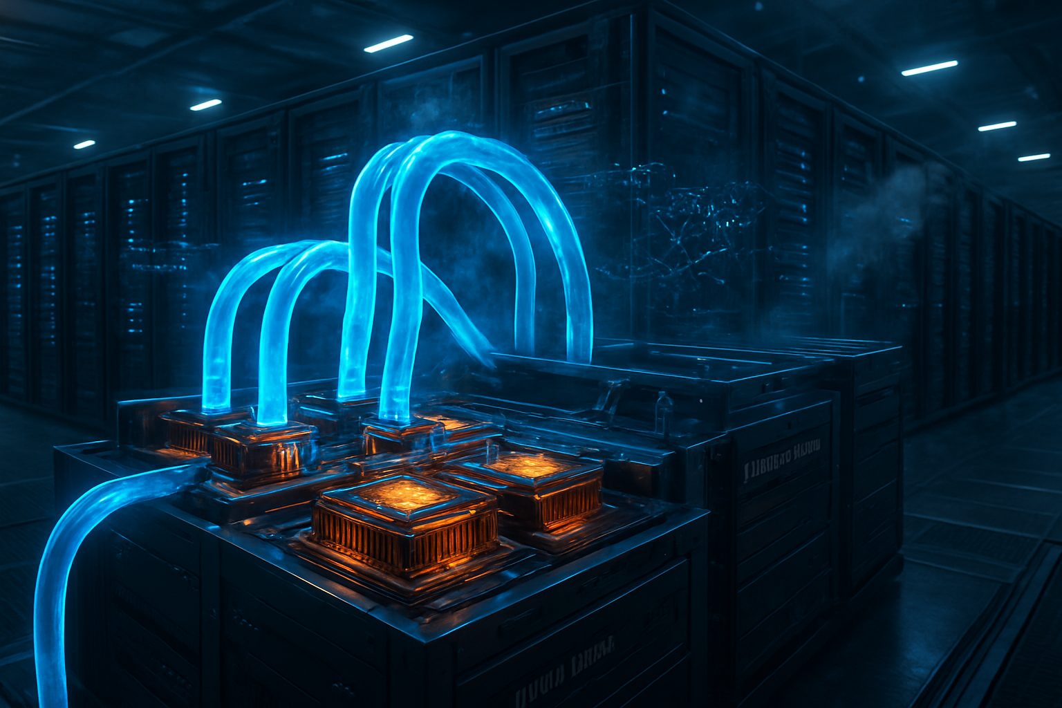
    To solve this, manufacturers have turned to Direct-to-Chip (D2C) liquid cooling. This technology utilizes specialized "cold plates" made of high-conductivity copper that are mounted directly onto the GPUs and CPUs. A coolant—typically a mixture of water and propylene glycol like the industry-standard PG25—is pumped through these plates to absorb heat. Liquid is roughly 3,000 times more effective at heat transfer than air, allowing it to manage the 1,200W TDP of an NVIDIA B200 or the 1,400W peak output of the AMD (NASDAQ: AMD) Instinct MI355X. Initial reactions from the research community have been overwhelmingly positive, noting that liquid cooling not only prevents thermal throttling but also allows for more consistent clock speeds, which is critical for long-running LLM training jobs.

    The New Infrastructure Giants: Winners in the Liquid Cooling Race

    This shift has created a massive windfall for infrastructure providers who were once considered "boring" utility companies. Vertiv Holdings Co (NYSE: VRT) has emerged as a primary winner, serving as a key partner for NVIDIA’s Blackwell systems by providing the Coolant Distribution Units (CDUs) and manifolds required to manage the complex fluid loops. Similarly, Schneider Electric (OTC: SBGSY), after its strategic $850 million acquisition of Motivair in late 2024, has solidified its position as a leader in high-performance thermal management. These companies are no longer just selling racks; they are selling integrated liquid ecosystems.

    The competitive landscape for data center operators like Equinix, Inc. (NASDAQ: EQIX) and Digital Realty has also been disrupted. Legacy data centers designed for air cooling are facing expensive retrofitting challenges, while "greenfield" sites built specifically for liquid cooling are seeing unprecedented demand. Server OEMs like Super Micro Computer, Inc. (NASDAQ: SMCI) and Dell Technologies Inc. (NYSE: DELL) have also had to pivot, with Supermicro reporting that over half of its AI server shipments in 2025 now feature liquid cooling as the default configuration. This transition has effectively created a two-tier market: those with liquid-ready facilities and those left behind with aging, air-cooled hardware.

    Sustainability and the Global AI Landscape

    Beyond the technical necessity, the mandatory adoption of liquid cooling is having a profound impact on the broader AI landscape’s environmental footprint. Traditional data centers are notorious water consumers, often using evaporative cooling towers that lose millions of gallons of water to the atmosphere. Modern liquid-cooled designs are often "closed-loop," significantly reducing water consumption by up to 70%. Furthermore, the Power Usage Effectiveness (PUE) of liquid-cooled facilities is frequently below 1.1, a massive improvement over the 1.5 to 2.0 PUE seen in older air-cooled sites.

    However, this transition is not without its concerns. The sheer power density of these new racks is putting immense strain on local power grids. While liquid cooling is more efficient, the total energy demand of a 140kW rack is still immense. This has led to comparisons with the mainframe era of the 1960s and 70s, where computers were similarly water-cooled and required dedicated power substations. The difference today is the scale; rather than one mainframe per company, we are seeing thousands of these high-density racks deployed in massive clusters, leading to a "power grab" where AI labs are competing for access to high-capacity electrical grids.

    Looking Ahead: From 140kW to 1 Megawatt Racks

    The transition to liquid cooling is far from over. Experts predict that the next generation of AI chips, such as NVIDIA’s projected "Rubin" architecture, will push rack densities even further. We are already seeing the first pilot programs for 250kW racks, and some modular data center designs are targeting 1-megawatt clusters within a single enclosure by 2027. This will likely necessitate a shift from Direct-to-Chip cooling to "Immersion Cooling," where entire server blades are submerged in non-conductive, dielectric fluids.

    The challenges remaining are largely operational. Standardizing "Universal Quick Disconnect" (UQD) connectors to ensure leak-proof maintenance is a top priority for the Open Compute Project (OCP). Additionally, the industry must train a new generation of data center technicians who are as comfortable with plumbing and fluid dynamics as they are with networking and software. As AI models continue to grow in complexity, the hardware that supports them must become increasingly exotic, moving further away from the traditional server room and closer to a high-tech industrial chemical plant.

    A New Paradigm for the AI Era

    The mandatory shift to liquid cooling marks the end of the "commodity" data center. In 2025, the facility itself has become as much a part of the AI stack as the software or the silicon. The ability to move heat efficiently is now a primary bottleneck for AI progress, and those who master the liquid-cooled paradigm will have a significant strategic advantage in the years to come.

    As we move into 2026, watch for further consolidation in the cooling market and the emergence of new standards for "heat reuse," where the waste heat from AI data centers is used to provide district heating for nearby cities. The transition from air to liquid is more than just a technical upgrade; it is a fundamental redesign of the physical foundation of the digital world, necessitated by our insatiable hunger for artificial intelligence.


    This content is intended for informational purposes only and represents analysis of current AI developments.

    TokenRing AI delivers enterprise-grade solutions for multi-agent AI workflow orchestration, AI-powered development tools, and seamless remote collaboration platforms.
    For more information, visit https://www.tokenring.ai/.

  • AI Chip Wars Escalate: Nvidia’s Blackwell Unleashes Trillion-Parameter Power as Qualcomm Enters the Data Center Fray

    AI Chip Wars Escalate: Nvidia’s Blackwell Unleashes Trillion-Parameter Power as Qualcomm Enters the Data Center Fray

    The artificial intelligence landscape is witnessing an unprecedented acceleration in hardware innovation, with two industry titans, Nvidia (NASDAQ: NVDA) and Qualcomm (NASDAQ: QCOM), spearheading the charge with their latest AI chip architectures. Nvidia's Blackwell platform, featuring the groundbreaking GB200 Grace Blackwell Superchip and fifth-generation NVLink, is already rolling out, promising up to a 30x performance leap for large language model (LLM) inference. Simultaneously, Qualcomm has officially thrown its hat into the AI data center ring with the announcement of its AI200 and AI250 chips, signaling a strategic and potent challenge to Nvidia's established dominance by focusing on power-efficient, cost-effective rack-scale AI inference.

    As of late 2024 and early 2025, these developments are not merely incremental upgrades but represent foundational shifts in how AI models will be trained, deployed, and scaled. Nvidia's Blackwell is poised to solidify its leadership in high-end AI training and inference, catering to the insatiable demand from hyperscalers and major AI labs. Meanwhile, Qualcomm's strategic entry, though with commercial availability slated for 2026 and 2027, has already sent ripples through the market, promising a future of intensified competition, diverse choices for enterprises, and potentially lower total cost of ownership for deploying generative AI at scale. The immediate impact is a palpable surge in AI processing capabilities, setting the stage for more complex, efficient, and accessible AI applications across industries.

    A Technical Deep Dive into Next-Generation AI Architectures

    Nvidia's Blackwell architecture, named after the pioneering mathematician David Blackwell, represents a monumental leap in GPU design, engineered to power the next generation of AI and accelerated computing. At its core is the Blackwell GPU, the largest ever produced by Nvidia, boasting an astonishing 208 billion transistors fabricated on TSMC's custom 4NP process. This GPU employs an innovative dual-die design, where two massive dies function cohesively as a single unit, interconnected by a blazing-fast 10 TB/s NV-HBI interface. A single Blackwell GPU can deliver up to 20 petaFLOPS of FP4 compute power. The true powerhouse, however, is the GB200 Grace Blackwell Superchip, which integrates two Blackwell Tensor Core GPUs with an Nvidia Grace CPU, leveraging NVLink-C2C for 900 GB/s bidirectional bandwidth. This integration, along with 192 GB of HBM3e memory providing 8 TB/s bandwidth per B200 GPU, sets a new standard for memory-intensive AI workloads.

    A cornerstone of Blackwell's scalability is the fifth-generation NVLink, which doubles the bandwidth of its predecessor to 1.8 TB/s bidirectional throughput per GPU. This allows for seamless, high-speed communication across an astounding 576 GPUs, a necessity for training and deploying trillion-parameter AI models. The NVLink Switch further extends this interconnect across multiple servers, enabling model parallelism across vast GPU clusters. The flagship GB200 NVL72 is a liquid-cooled, rack-scale system comprising 36 GB200 Superchips, effectively creating a single, massive GPU cluster capable of 1.44 exaFLOPS (FP4) of compute performance. Blackwell also introduces a second-generation Transformer Engine that accelerates LLM inference and training, supporting new precisions like 8-bit floating point (FP8) and a novel 4-bit floating point (NVFP4) format, while leveraging advanced dynamic range management for accuracy. This architecture offers a staggering 30 times faster real-time inference for trillion-parameter LLMs and 4 times faster training compared to H100-based systems, all while reducing energy consumption per inference by up to 25 times.

    In stark contrast, Qualcomm's AI200 and AI250 chips are purpose-built for rack-scale AI inference in data centers, with a strong emphasis on power efficiency, cost-effectiveness, and memory capacity for generative AI. While Nvidia targets the full spectrum of AI, from training to inference at the highest scale, Qualcomm strategically aims to disrupt the burgeoning inference market. The AI200 and AI250 chips leverage Qualcomm's deep expertise in mobile NPU technology, incorporating the Qualcomm AI Engine which includes the Hexagon NPU, Adreno GPU, and Kryo/Oryon CPU. A standout innovation in the AI250 is its "near-memory computing" (NMC) architecture, which Qualcomm claims delivers over 10 times the effective memory bandwidth and significantly lower power consumption by minimizing data movement.

    Both the AI200 and AI250 utilize high-capacity LPDDR memory, with the AI200 supporting an impressive 768 GB per card. This choice of LPDDR provides greater memory capacity at a lower cost, crucial for the memory-intensive requirements of large language models and multimodal models, especially for large-context-window applications. Qualcomm's focus is on optimizing performance per dollar per watt, aiming to drastically reduce the total cost of ownership (TCO) for data centers. Their rack solutions feature direct liquid cooling and are designed for both scale-up (PCIe) and scale-out (Ethernet) capabilities. The AI research community and industry experts have largely applauded Nvidia's Blackwell as a continuation of its technological dominance, solidifying its "strategic moat" with CUDA and continuous innovation. Qualcomm's entry, while not yet delivering commercially available chips, is viewed as a bold and credible challenge, with its focus on TCO and power efficiency offering a compelling alternative for enterprises, potentially diversifying the AI hardware landscape and intensifying competition.

    Industry Impact: Shifting Sands in the AI Hardware Arena

    The introduction of Nvidia's Blackwell and Qualcomm's AI200/AI250 chips is poised to reshape the competitive landscape for AI companies, tech giants, and startups alike. Nvidia's (NASDAQ: NVDA) Blackwell platform, with its unprecedented performance gains and scalability, primarily benefits hyperscale cloud providers like Microsoft (NASDAQ: MSFT), Amazon (NASDAQ: AMZN), Google (NASDAQ: GOOGL), and Meta (NASDAQ: META), who are at the forefront of AI model development and deployment. These companies, already Nvidia's largest customers, will leverage Blackwell to train even larger and more complex models, accelerating their AI research and product roadmaps. Server makers and leading AI companies also stand to gain immensely from the increased throughput and energy efficiency, allowing them to offer more powerful and cost-effective AI services. This solidifies Nvidia's strategic advantage in the high-end AI training market, particularly outside of China due to export restrictions, ensuring its continued leadership in the AI supercycle.

    Qualcomm's (NASDAQ: QCOM) strategic entry into the data center AI inference market with the AI200/AI250 chips presents a significant competitive implication. While Nvidia has a strong hold on both training and inference, Qualcomm is directly targeting the rapidly expanding AI inference segment, which is expected to constitute a larger portion of AI workloads in the future. Qualcomm's emphasis on power efficiency, lower total cost of ownership (TCO), and high memory capacity through LPDDR memory and near-memory computing offers a compelling alternative for enterprises and cloud providers looking to deploy generative AI at scale more economically. This could disrupt existing inference solutions by providing a more cost-effective and energy-efficient option, potentially leading to a more diversified supplier base and reduced reliance on a single vendor.

    The competitive implications extend beyond just Nvidia and Qualcomm. Other AI chip developers, such as AMD (NASDAQ: AMD), Intel (NASDAQ: INTC), and various startups, will face increased pressure to innovate and differentiate their offerings. Qualcomm's move signals a broader trend of specialized hardware for AI workloads, potentially leading to a more fragmented but ultimately more efficient market. Companies that can effectively integrate these new chip architectures into their existing infrastructure or develop new services leveraging their unique capabilities will gain significant market positioning and strategic advantages. The potential for lower inference costs could also democratize access to advanced AI, enabling a wider range of startups and smaller enterprises to deploy sophisticated AI models without prohibitive hardware expenses, thereby fostering further innovation across the industry.

    Wider Significance: Reshaping the AI Landscape and Addressing Grand Challenges

    The introduction of Nvidia's Blackwell and Qualcomm's AI200/AI250 chips signifies a profound evolution in the broader AI landscape, addressing critical trends such as the relentless pursuit of larger AI models, the urgent need for energy efficiency, and the ongoing efforts towards the democratization of AI. Nvidia's Blackwell architecture, with its capability to handle trillion-parameter and multi-trillion-parameter models, is explicitly designed to be the cornerstone for the next era of high-performance AI infrastructure. This directly accelerates the development and deployment of increasingly complex generative AI, data analytics, and high-performance computing (HPC) workloads, pushing the boundaries of what AI can achieve. Its superior processing speed and efficiency also tackle the growing concern of AI's energy footprint; Nvidia highlights that training ultra-large AI models with 2,000 Blackwell GPUs would consume 4 megawatts over 90 days, a stark contrast to 15 megawatts for 8,000 older GPUs, demonstrating a significant leap in power efficiency.

    Qualcomm's AI200/AI250 chips, while focused on inference, also contribute significantly to these trends. By prioritizing power efficiency and a lower Total Cost of Ownership (TCO), Qualcomm aims to democratize access to high-performance AI inference, challenging the traditional reliance on general-purpose GPUs for all AI workloads. Their architecture, optimized for running large language models (LLMs) and multimodal models (LMMs) efficiently, is crucial for the increasing demand for real-time generative AI applications in data centers. The AI250's near-memory computing architecture, promising over 10 times higher effective memory bandwidth and significantly reduced power consumption, directly addresses the memory wall problem and the escalating energy demands of AI. Both companies, through their distinct approaches, are enabling the continued growth of sophisticated generative AI models, addressing the critical need for energy efficiency, and striving to make powerful AI capabilities more accessible.

    However, these advancements are not without potential concerns. The sheer computational power and high-density designs of these new chips translate to substantial power requirements. High-density racks with Blackwell GPUs, for instance, can demand 60kW to 120kW, and Qualcomm's racks draw 160 kW, necessitating advanced cooling solutions like liquid cooling. This stresses existing electrical grids and raises significant environmental questions. The cutting-edge nature and performance also come with a high price tag, potentially creating an "AI divide" where smaller research groups and startups might struggle to access these transformative technologies. Furthermore, Nvidia's robust CUDA software ecosystem, while a major strength, can contribute to vendor lock-in, posing a challenge for competitors and hindering diversification in the AI software stack. Geopolitical factors, such as export controls on advanced semiconductors, also loom large, impacting global availability and adoption.

    Comparing these to previous AI milestones reveals both evolutionary and revolutionary steps. Blackwell represents a dramatic extension of previous GPU generations like Hopper and Ampere, introducing FP4 precision and a second-generation Transformer Engine specifically to tackle the scaling challenges of modern LLMs, which were not as prominent in earlier designs. The emphasis on massive multi-GPU scaling with enhanced NVLink for trillion-parameter models pushes boundaries far beyond what was feasible even a few years ago. Qualcomm's entry as an inference specialist, leveraging its mobile NPU heritage, marks a significant diversification of the AI chip market. This specialization, reminiscent of Google's Tensor Processing Units (TPUs), signals a maturing AI hardware market where dedicated solutions can offer substantial advantages in TCO and efficiency for production deployment, challenging the GPU's sole dominance in certain segments. Both companies' move towards delivering integrated, rack-scale AI systems, rather than just individual chips, also reflects the immense computational and communication demands of today's AI workloads, marking a new era in AI infrastructure development.

    Future Developments: The Road Ahead for AI Silicon

    The trajectory of AI chip architecture is one of relentless innovation, with both Nvidia and Qualcomm already charting ambitious roadmaps that extend far beyond their current offerings. For Nvidia (NASDAQ: NVDA), the Blackwell platform, while revolutionary, is just a stepping stone. The near-term will see the release of Blackwell Ultra (B300 series) in the second half of 2025, promising enhanced compute performance and a significant boost to 288GB of HBM3E memory. Nvidia has committed to an annual release cadence for its data center platforms, with major new architectures every two years and "Ultra" updates in between, ensuring a continuous stream of advancements. These chips are set to drive massive investments in data centers and cloud infrastructure, accelerating generative AI, scientific computing, advanced manufacturing, and large-scale simulations, forming the backbone of future "AI factories" and agentic AI platforms.

    Looking further ahead, Nvidia's next-generation architecture, Rubin, named after astrophysicist Vera Rubin, is already in the pipeline. The Rubin GPU and its companion CPU, Vera, are scheduled for mass production in late 2025 and will be available in early 2026. Manufactured by TSMC using a 3nm process node and featuring HBM4 memory, Rubin is projected to offer 50 petaflops of performance in FP4, a substantial increase from Blackwell's 20 petaflops. An even more powerful Rubin Ultra is planned for 2027, expected to double Rubin's performance to 100 petaflops and deliver up to 15 ExaFLOPS of FP4 inference compute in a full rack configuration. Rubin will also incorporate NVLink 6 switches (3600 GB/s) and CX9 network cards (1,600 Gb/s) to support unprecedented data transfer needs. Experts predict Rubin will be a significant step towards Artificial General Intelligence (AGI) and is already slated for use in supercomputers like Los Alamos National Laboratory's Mission and Vision systems. Challenges for Nvidia include navigating geopolitical tensions and export controls, maintaining its technological lead through continuous R&D, and addressing the escalating power and cooling demands of "gigawatt AI factories."

    Qualcomm (NASDAQ: QCOM), while entering the data center market with the AI200 (commercial availability in 2026) and AI250 (2027), also has a clear and aggressive strategic roadmap. The AI200 will support 768GB of LPDDR memory per card for cost-effective, high-capacity inference. The AI250 will introduce an innovative near-memory computing architecture, promising over 10 times higher effective memory bandwidth and significantly lower power consumption, marking a generational leap in efficiency for AI inference workloads. Qualcomm is committed to an annual cadence for its data center roadmap, focusing on industry-leading AI inference performance, energy efficiency, and total cost of ownership (TCO). These chips are primarily optimized for demanding inference workloads such as large language models, multimodal models, and generative AI tools. Early deployments include a partnership with Saudi Arabia's Humain, which plans to deploy 200 megawatts of data center racks powered by AI200 chips starting in 2026.

    Qualcomm's broader AI strategy aims for "intelligent computing everywhere," extending beyond data centers to encompass hybrid, personalized, and agentic AI across mobile, PC, wearables, and automotive devices. This involves always-on sensing and personalized knowledge graphs to enable proactive, contextually-aware AI assistants. The main challenges for Qualcomm include overcoming Nvidia's entrenched market dominance (currently over 90%), clearly validating its promised performance and efficiency gains, and building a robust developer ecosystem comparable to Nvidia's CUDA. However, experts like Qualcomm CEO Cristiano Amon believe the AI market is rapidly becoming competitive, and companies investing in efficient architectures will be well-positioned for the long term. The long-term future of AI chip architectures will likely be a hybrid landscape, utilizing a mixture of GPUs, ASICs, FPGAs, and entirely new chip architectures tailored to specific AI workloads, with innovations like silicon photonics and continued emphasis on disaggregated compute and memory resources driving efficiency and bandwidth gains. The global AI chip market is projected to reach US$257.6 billion by 2033, underscoring the immense investment and innovation yet to come.

    Comprehensive Wrap-up: A New Era of AI Silicon

    The advent of Nvidia's Blackwell and Qualcomm's AI200/AI250 chips marks a pivotal moment in the evolution of artificial intelligence hardware. Nvidia's Blackwell platform, with its GB200 Grace Blackwell Superchip and fifth-generation NVLink, is a testament to the pursuit of extreme-scale AI, delivering unprecedented performance and efficiency for trillion-parameter models. Its 208 billion transistors, advanced Transformer Engine, and rack-scale system architecture are designed to power the most demanding AI training and inference workloads, solidifying Nvidia's (NASDAQ: NVDA) position as the dominant force in high-performance AI. In parallel, Qualcomm's (NASDAQ: QCOM) AI200/AI250 chips represent a strategic and ambitious entry into the data center AI inference market, leveraging the company's mobile DNA to offer highly energy-efficient and cost-effective solutions for large language models and multimodal inference at scale.

    Historically, Nvidia's journey from gaming GPUs to the foundational CUDA platform and now Blackwell, has consistently driven the advancements in deep learning. Blackwell is not just an upgrade; it's engineered for the "generative AI era," explicitly tackling the scale and complexity that define today's AI breakthroughs. Qualcomm's AI200/AI250, building on its Cloud AI 100 Ultra lineage, signifies a crucial diversification beyond its traditional smartphone market, positioning itself as a formidable contender in the rapidly expanding AI inference segment. This shift is historically significant as it introduces a powerful alternative focused on sustainability and economic efficiency, challenging the long-standing dominance of general-purpose GPUs across all AI workloads.

    The long-term impact of these architectures will likely see a bifurcated but symbiotic AI hardware ecosystem. Blackwell will continue to drive the cutting edge of AI research, enabling the training of ever-larger and more complex models, fueling unprecedented capital expenditure from hyperscalers and sovereign AI initiatives. Its continuous innovation cycle, with the Rubin architecture already on the horizon, ensures Nvidia will remain at the forefront of AI computing. Qualcomm's AI200/AI250, conversely, could fundamentally reshape the AI inference landscape. By offering a compelling alternative that prioritizes sustainability and economic efficiency, it addresses the critical need for cost-effective, widespread AI deployment. As AI becomes ubiquitous, the sheer volume of inference tasks will demand highly efficient solutions, where Qualcomm's offerings could gain significant traction, diversifying the competitive landscape and making AI more accessible and sustainable.

    In the coming weeks and months, several key indicators will reveal the trajectory of these innovations. For Nvidia Blackwell, watch for updates in upcoming earnings reports (such as Q3 FY2026, scheduled for November 19, 2025) regarding the Blackwell Ultra ramp and overall AI infrastructure backlog. The adoption rates by major hyperscalers and sovereign AI initiatives, alongside any further developments on "downgraded" Blackwell variants for the Chinese market, will be crucial. For Qualcomm AI200/AI250, the focus will be on official shipping announcements and initial deployment reports, particularly the success of partnerships with companies like Hewlett Packard Enterprise (HPE) and Core42. Crucially, independent benchmarks and MLPerf results will be vital to validate Qualcomm's claims regarding capacity, energy efficiency, and TCO, shaping its competitive standing against Nvidia's inference offerings. Both companies' ongoing development of their AI software ecosystems and any new product roadmap announcements will also be critical for developer adoption and future market dynamics.


    This content is intended for informational purposes only and represents analysis of current AI developments.

    TokenRing AI delivers enterprise-grade solutions for multi-agent AI workflow orchestration, AI-powered development tools, and seamless remote collaboration platforms.
    For more information, visit https://www.tokenring.ai/.

  • US Solidifies AI Chip Embargo: Blackwell Ban on China Intensifies Global Tech Race

    US Solidifies AI Chip Embargo: Blackwell Ban on China Intensifies Global Tech Race

    Washington D.C., November 4, 2025 – The White House has unequivocally reaffirmed its ban on the export of advanced AI chips, specifically Nvidia's (NASDAQ: NVDA) cutting-edge Blackwell series, to China. This decisive move, announced days before and solidified today, marks a significant escalation in the ongoing technological rivalry between the United States and China, sending ripples across the global artificial intelligence landscape and prompting immediate reactions from industry leaders and geopolitical observers alike. The Biden administration's stance underscores a strategic imperative to safeguard American AI supremacy and national security interests, effectively drawing a clear line in the silicon sands of the burgeoning AI arms race.

    This reaffirmation is not merely a continuation but a hardening of existing export controls, signaling Washington's resolve to prioritize long-term strategic advantages over immediate economic gains for American semiconductor companies. The ban is poised to profoundly impact China's ambitious AI development programs, forcing a rapid recalibration towards indigenous solutions and potentially creating a bifurcated global AI ecosystem. As the world grapples with the implications of this technological decoupling, the focus shifts to how both nations will navigate this intensified competition and what it means for the future of artificial intelligence innovation.

    The Blackwell Blockade: Technical Prowess Meets Geopolitical Walls

    Nvidia's Blackwell architecture represents the pinnacle of current AI chip technology, designed to power the next generation of generative AI and large language models (LLMs) with unprecedented performance. The Blackwell series, including chips like the GB200 Grace Blackwell Superchip, boasts significant advancements over its predecessors, such as the Hopper (H100) architecture. Key technical specifications and capabilities include:

    • Massive Scale and Performance: Blackwell chips are engineered for trillion-parameter AI models, offering up to 20 petaFLOPS of FP4 AI performance per GPU. This represents a substantial leap in computational power, crucial for training and deploying increasingly complex AI systems.
    • Second-Generation Transformer Engine: The architecture features a refined Transformer Engine that supports new data types like FP6, enhancing performance for LLMs while maintaining accuracy.
    • NVLink 5.0: Blackwell introduces a fifth generation of NVLink, providing 1.8 terabytes per second (TB/s) of bidirectional throughput per GPU, allowing for seamless communication between thousands of GPUs in a single cluster. This is vital for distributed AI training at scale.
    • Dedicated Decompression Engine: Built-in hardware decompression accelerates data processing, a critical bottleneck in large-scale AI workloads.
    • Enhanced Reliability and Diagnostics: Features like a Reliability, Availability, and Serviceability (RAS) engine and advanced diagnostics ensure higher uptime and easier maintenance for massive AI data centers.

    The significant difference from previous approaches lies in Blackwell's holistic design for the exascale AI era, where models are too large for single GPUs and require massive, interconnected systems. While previous chips like the H100 were powerful, Blackwell pushes the boundaries of interconnectivity, memory bandwidth, and raw compute specifically tailored for the demands of next-generation AI. Initial reactions from the AI research community and industry experts have highlighted Blackwell as a "game-changer" for AI development, capable of unlocking new frontiers in model complexity and application. However, these same experts also acknowledge the geopolitical reality that such advanced technology inevitably becomes a strategic asset in national competition. The ban ensures that this critical hardware advantage remains exclusively within the US and its allies, aiming to create a significant performance gap that China will struggle to bridge independently.

    Shifting Sands: Impact on AI Companies and the Global Tech Ecosystem

    The White House's Blackwell ban has immediate and far-reaching implications for AI companies, tech giants, and startups globally. For Nvidia (NASDAQ: NVDA), the direct impact is a significant loss of potential revenue from the lucrative Chinese market, which historically accounted for a substantial portion of its data center sales. While Nvidia CEO Jensen Huang has previously advocated for market access, the company has also been proactive in developing "hobbled" chips like the H20 for China to comply with previous restrictions. However, the definitive ban on Blackwell suggests even these modified versions may not be viable for the most advanced architectures. Despite this, soaring demand from American AI companies and other allied nations is expected to largely offset these losses in the near term, demonstrating the robust global appetite for Nvidia's technology.

    Chinese AI companies, including giants like Baidu (NASDAQ: BIDU), Alibaba (NYSE: BABA), and numerous startups, face the most immediate and acute challenges. Without access to state-of-the-art Blackwell chips, they will be forced to rely on older, less powerful hardware, or significantly accelerate their efforts in developing domestic alternatives. This could lead to a "3-5 year lag" in AI performance compared to their US counterparts, impacting their ability to train and deploy advanced generative AI models, which are critical for various applications from cloud services to autonomous driving. This situation also creates an urgent impetus for Chinese semiconductor manufacturers like SMIC (SHA: 688981) and Huawei to rapidly innovate, though closing the technological gap with Nvidia will be an immense undertaking.

    Competitively, US AI labs and tech companies like Google (NASDAQ: GOOGL), Microsoft (NASDAQ: MSFT), Meta Platforms (NASDAQ: META), and various well-funded startups stand to benefit significantly. With exclusive access to Blackwell's unparalleled computational power, they can push the boundaries of AI research and development unhindered, accelerating breakthroughs in areas like foundation models, AI agents, and advanced robotics. This provides a strategic advantage in the global AI race, potentially disrupting existing products and services by enabling capabilities that are inaccessible to competitors operating under hardware constraints. The market positioning solidifies the US as the leading innovator in AI hardware and, by extension, advanced AI software development, reinforcing its strategic advantage in the evolving global tech landscape.

    Geopolitical Fault Lines: Wider Significance in the AI Landscape

    The Blackwell ban is more than just a trade restriction; it is a profound geopolitical statement that significantly reshapes the broader AI landscape and global power dynamics. This move fits squarely into the accelerating trend of technological decoupling between the United States and China, transforming AI into a critical battleground for economic, military, and ideological supremacy. It signifies a "hard turn" in US tech policy, where national security concerns and the maintenance of technological leadership take precedence over the principles of free trade and global economic integration.

    The primary impact is the deepening of the "AI arms race." By denying China access to the most advanced chips, the US aims to slow China's progress in developing sophisticated AI applications that could have military implications, such as advanced surveillance, autonomous weapons systems, and enhanced cyber capabilities. This policy is explicitly framed as an "AI defense measure," echoing Cold War-era technology embargoes and highlighting the strategic intent for technological containment. Concerns from US officials are that unrestricted access to Blackwell chips could meaningfully narrow or even erase the US lead in AI compute, a lead deemed essential for maintaining strategic advantage.

    However, this strategy also carries potential concerns and unintended consequences. While it aims to hobble China's immediate AI advancements, it simultaneously incentivizes Beijing to redouble its efforts in indigenous chip design and manufacturing. This could lead to the emergence of robust domestic alternatives in hardware, software, and AI training regimes that could make future re-entry for US companies even more challenging. The ban also risks creating a truly bifurcated global AI ecosystem, where different standards, hardware, and software stacks emerge, complicating international collaboration and potentially fragmenting the pace of global AI innovation. This move is a clear comparison to previous AI milestones where access to compute power has been a critical determinant of progress, but now with an explicit geopolitical overlay.

    The Road Ahead: Future Developments and Expert Predictions

    Looking ahead, the Blackwell ban is expected to trigger several significant near-term and long-term developments in the AI and semiconductor industries. In the near term, Chinese AI companies will likely intensify their focus on optimizing existing, less powerful hardware and investing heavily in domestic chip design. This could lead to a surge in demand for older-generation chips from other manufacturers or a rapid acceleration in the development of custom AI accelerators tailored to specific Chinese applications. We can also anticipate a heightened focus on software-level optimizations and model compression techniques to maximize the utility of available hardware.

    In the long term, this ban will undoubtedly accelerate China's ambition to achieve complete self-sufficiency in advanced semiconductor manufacturing. Billions will be poured into research and development, foundry expansion, and talent acquisition within China, aiming to close the technological gap with companies like Nvidia and TSMC (NYSE: TSM). This could lead to the emergence of formidable Chinese competitors in the AI chip space over the next decade. Potential applications and use cases on the horizon for the US and its allies, with exclusive access to Blackwell, include the deployment of truly intelligent AI agents, advancements in scientific discovery through AI-driven simulations, and the development of highly sophisticated autonomous systems across various sectors.

    However, significant challenges need to be addressed. For the US, maintaining its technological lead requires sustained investment in R&D, fostering a robust domestic semiconductor ecosystem, and attracting top global talent. For China, the challenge is immense: overcoming fundamental physics and engineering hurdles, scaling manufacturing capabilities, and building a comprehensive software ecosystem around new hardware. Experts predict that while China will face considerable headwinds, its determination to achieve technological independence should not be underestimated. The next few years will likely see a fierce race in semiconductor innovation, with both nations striving for breakthroughs that could redefine the global technological balance.

    A New Era of AI Geopolitics: A Comprehensive Wrap-Up

    The White House's unwavering stance on banning Nvidia Blackwell chip sales to China marks a watershed moment in the history of artificial intelligence and global geopolitics. The key takeaway is clear: advanced AI hardware is now firmly entrenched as a strategic asset, subject to national security interests and geopolitical competition. This decision solidifies a bifurcated technological future, where access to cutting-edge compute power will increasingly define national capabilities in AI.

    This development's significance in AI history cannot be overstated. It moves beyond traditional economic competition into a realm of strategic technological containment, fundamentally altering how AI innovation will unfold globally. For the United States, it aims to preserve its leadership in the most transformative technology of our era. For China, it presents an unprecedented challenge and a powerful impetus to accelerate its indigenous innovation efforts, potentially reshaping its domestic tech industry for decades to come.

    Final thoughts on the long-term impact suggest a more fragmented global AI landscape, potentially leading to divergent technological paths and standards. While this might slow down certain aspects of global AI collaboration, it will undoubtedly spur innovation within each bloc as nations strive for self-sufficiency and competitive advantage. What to watch for in the coming weeks and months includes China's official responses and policy adjustments, the pace of its domestic chip development, and how Nvidia and other US tech companies adapt their strategies to this new geopolitical reality. The AI war has indeed entered a new and irreversible phase, with the battle lines drawn in silicon.


    This content is intended for informational purposes only and represents analysis of current AI developments.

    TokenRing AI delivers enterprise-grade solutions for multi-agent AI workflow orchestration, AI-powered development tools, and seamless remote collaboration platforms.
    For more information, visit https://www.tokenring.ai/.