As of February 5, 2026, the semiconductor industry has officially entered the era of "Bumpless" silicon. The long-anticipated transition from traditional solder-based microbumps to direct copper-to-copper (Cu-Cu) hybrid bonding has reached a critical tipping point, with Taiwan Semiconductor Manufacturing Co. (NYSE: TSM) announcing that its System on Integrated Chips (SoIC) technology has successfully achieved high-volume manufacturing (HVM) at a 6-micrometer bond pitch. This milestone represents a tectonic shift in how the world’s most powerful processors are built, moving beyond the physical limits of two-dimensional scaling into a fully integrated 3D landscape.
The immediate significance of this development cannot be overstated. By eliminating the bulky solder "bumps" that have connected chips for decades, TSMC has unlocked a 100x increase in interconnect density and a dramatic reduction in power consumption. This breakthrough serves as the foundational architecture for the industry’s most ambitious AI accelerators, including the newly debuted NVIDIA (NASDAQ: NVDA) Rubin series and the AMD (NASDAQ: AMD) Instinct MI400. In an era where AI training clusters consume gigawatts of power, the ability to move data between logic and memory with nearly zero resistance is no longer a luxury—it is a requirement for the continued survival of Moore’s Law.
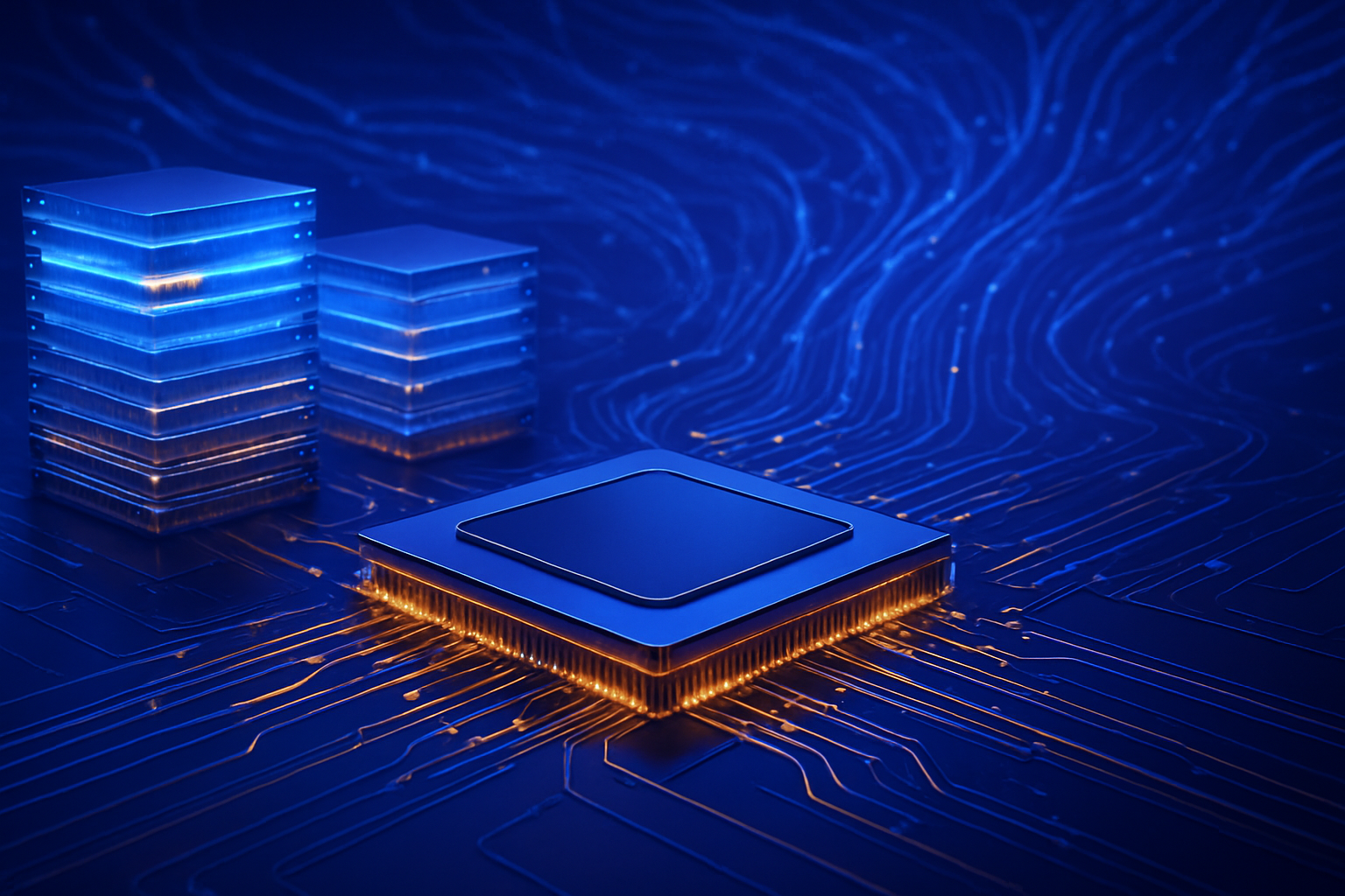
The Death of the Microbump: Engineering the 6-Micrometer Interface
At the heart of this revolution is TSMC’s SoIC-X (bumpless) technology. For years, the industry relied on "microbumps"—tiny spheres of solder roughly 30 to 40 micrometers in diameter—to stack chips. However, as AI models grew, these bumps became a bottleneck; they were too large to allow for the thousands of simultaneous connections required for high-bandwidth data transfer and contributed significant electrical parasitics. TSMC’s 6-micrometer hybrid bonding process replaces these bumps with a direct, atomic-level fusion of copper pads. The process begins with Chemical Mechanical Polishing (CMP) to achieve a surface flatness with less than 0.5 nanometers of roughness, followed by plasma activation of the dielectric surface. When two wafers are pressed together at room temperature and subsequently annealed at 200°C, the copper pads expand and fuse into a single, continuous metal path.
This "bumpless" architecture allows for a staggering density of 25,000 to 50,000 interconnects per square millimeter, compared to the roughly 600–1,000 interconnects possible with standard microbumps. By shrinking the bond pitch to 6 micrometers, TSMC has effectively turned 3D chip stacks into a single, monolithic piece of silicon from an electrical perspective. Initial reactions from the AI research community have been electric, with experts noting that the vertical distance between dies is now so small that signal latency has effectively vanished, allowing for "logic-on-logic" stacking that behaves as if it were a single, giant processor.
The technical specifications of this leap are already manifesting in hardware. The NVIDIA Rubin platform, announced just weeks ago, utilizes this 6µm SoIC-X architecture to integrate the "Vera" CPU and "Rubin" GPU with HBM4 memory. Because HBM4 uses a 2048-bit interface—double the width of the previous generation—it is physically incompatible with legacy microbump technology. Hybrid bonding is the only way to accommodate the sheer number of pins required to hit Rubin’s target memory bandwidth of 13 TB/s.
The Interconnect War: Market Dominance in Foundry 2.0
The successful scaling of 6µm hybrid bonding has solidified TSMC’s lead in what analysts are calling "Foundry 2.0"—a market where packaging is as important as transistor size. According to recent data from IDC, TSMC’s market share in advanced packaging is projected to reach 66% by the end of 2026. This dominance is driven by the fact that both NVIDIA and AMD have pivoted their entire flagship roadmaps to favor TSMC’s SoIC ecosystem. AMD’s Instinct MI400, built on the CDNA 5 architecture, leverages SoIC to stack a massive 432GB of HBM4 memory directly over its compute dies, achieving a "yotta-scale" foundation that AMD claims is 50% more dense than its previous generation.
However, the competition is not standing still. Intel (NASDAQ: INTC) is aggressively pushing its "Foveros Direct" technology, aiming to reach a sub-5-micrometer pitch by the second half of 2026 on its 18A-PT node. Intel’s strategy involves combining hybrid bonding with its "PowerVia" backside power delivery, a dual-pronged attack intended to win back hyperscaler customers like Microsoft (NASDAQ: MSFT) and Amazon (NASDAQ: AMZN) who are designing custom AI silicon. Meanwhile, Samsung Electronics (KRX: 005930) has launched its SAINT (Samsung Advanced Interconnect Technology) platform, specifically targeting the integration of its own HBM4 modules with logic dies in a "one-stop-shop" model that could appeal to cost-conscious AI labs.
The competitive implications are stark: companies unable to master hybrid bonding at the 6µm level or below risk being relegated to the mid-tier market. The strategic advantage for TSMC lies in its mature "3DFabric" ecosystem, which provides a standardized design flow for chiplet-based architectures. This has forced a shift in the industry where the "interconnect" is now the primary theater of competition, rather than the transistor gate itself.
Breaking the Memory Wall and the Power Efficiency Frontier
Beyond the corporate horse race, the hybrid bonding revolution addresses the two greatest crises in modern computing: the "Memory Wall" and the "Power Wall." For years, CPU and GPU speeds have outpaced the ability of memory to supply data, leading to wasted cycles and energy. By using 6µm hybrid bonding, designers can place memory directly on top of logic, reducing the distance data must travel from millimeters to micrometers. This results in a power efficiency of less than 0.05 picojoules per bit (pJ/bit)—a 3x to 10x improvement over 2.5D technologies like CoWoS and orders of magnitude better than traditional flip-chip packaging.
This shift fits into a broader trend of "Extreme Co-Design," where software, architecture, and packaging are developed in tandem. In the wider AI landscape, this means that the trillion-parameter models of 2026 can be trained on clusters that are physically smaller and significantly more energy-efficient than the massive data centers of the early 2020s. However, this advancement is not without concerns. The extreme precision required for 6µm bonding makes these chips incredibly difficult to repair; a single misaligned bond during the 200°C annealing process can result in the loss of multiple high-value dies, potentially keeping costs high for several more years.
Furthermore, the environmental impact of this technology is a double-edged sword. While the pJ/bit efficiency is a victory for sustainability, the increased performance is expected to trigger "Jevons Paradox," where the improved efficiency leads to an even greater total demand for AI compute, potentially offsetting any net energy savings at the global level.
Looking Ahead: The Path to 3 Micrometers and Beyond
The 6-micrometer milestone is merely a pitstop on TSMC’s roadmap. The company has already demonstrated prototypes of its "SoIC-Next" generation, which targets a 3-micrometer bond pitch for 2027. Experts predict that at the 3µm level, we will see the birth of "True 3D" processors, where different tiers of a single logic core are stacked on top of each other, allowing for clock speeds that were previously thought impossible due to thermal constraints.
We are also likely to see the emergence of an open chiplet ecosystem. With the implementation of the UCIe 2.0 (Universal Chiplet Interconnect Express) standard, 2026 and 2027 could see the first "mix-and-match" 3D stacks, where a specialized AI accelerator tile from a startup could be hybrid-bonded directly onto a base die from Intel or TSMC. The challenges remaining are primarily around thermal management and testing. Stacking multiple layers of high-power logic creates a "heat sandwich" that requires advanced liquid cooling or integrated microfluidic channels—technologies that are currently in the experimental phase but will become mandatory as we move toward 3µm pitches.
A New Dimension for Artificial Intelligence
The achievement of 6-micrometer hybrid bonding marks the definitive end of the "2D Silicon" era. In the history of artificial intelligence, this transition will likely be remembered as the moment when hardware finally caught up to the structural demands of neural networks. By mimicking the dense, three-dimensional connectivity of the human brain, hybrid-bonded chips are providing the physical substrate necessary for the next leap in machine intelligence.
In the coming months, the industry will be watching the yield rates of the NVIDIA Rubin and AMD MI400 very closely. If TSMC can maintain high yields at 6µm, the transition to 3D-first design will become irreversible, forcing a total reorganization of the semiconductor supply chain. For now, the "bumpless" revolution has given the AI industry a much-needed breath of fresh air, proving that even as we reach the atomic limits of the transistor, human ingenuity can always find another dimension in which to grow.
This content is intended for informational purposes only and represents analysis of current AI developments.
TokenRing AI delivers enterprise-grade solutions for multi-agent AI workflow orchestration, AI-powered development tools, and seamless remote collaboration platforms.
For more information, visit https://www.tokenring.ai/.