As of January 2026, the artificial intelligence industry has officially entered the "Rubin Era." Named after the pioneering astronomer Vera Rubin, NVIDIA’s latest architectural leap represents more than just a faster chip; it marks the transition of the data center from a collection of servers into a singular, planet-scale AI engine. This shift is being met by a massive infrastructure pivot from the world’s largest cloud providers, who are no longer content with off-the-shelf components. Instead, they are deploying "superfactories" and custom-designed ARM CPUs specifically engineered to squeeze every drop of performance out of NVIDIA’s silicon.
The immediate significance of this development cannot be overstated. We are witnessing the end of general-purpose computing as the primary driver of data center growth. In its place is a highly specialized, vertically integrated stack where the CPU, GPU, and networking fabric are co-designed at the atomic level. Microsoft’s "Fairwater" project and the latest custom ARM chips from AWS and Google are the first true examples of this "AI-first" infrastructure, promising to reduce the cost of training frontier models by orders of magnitude while enabling the rise of autonomous, agentic AI systems.
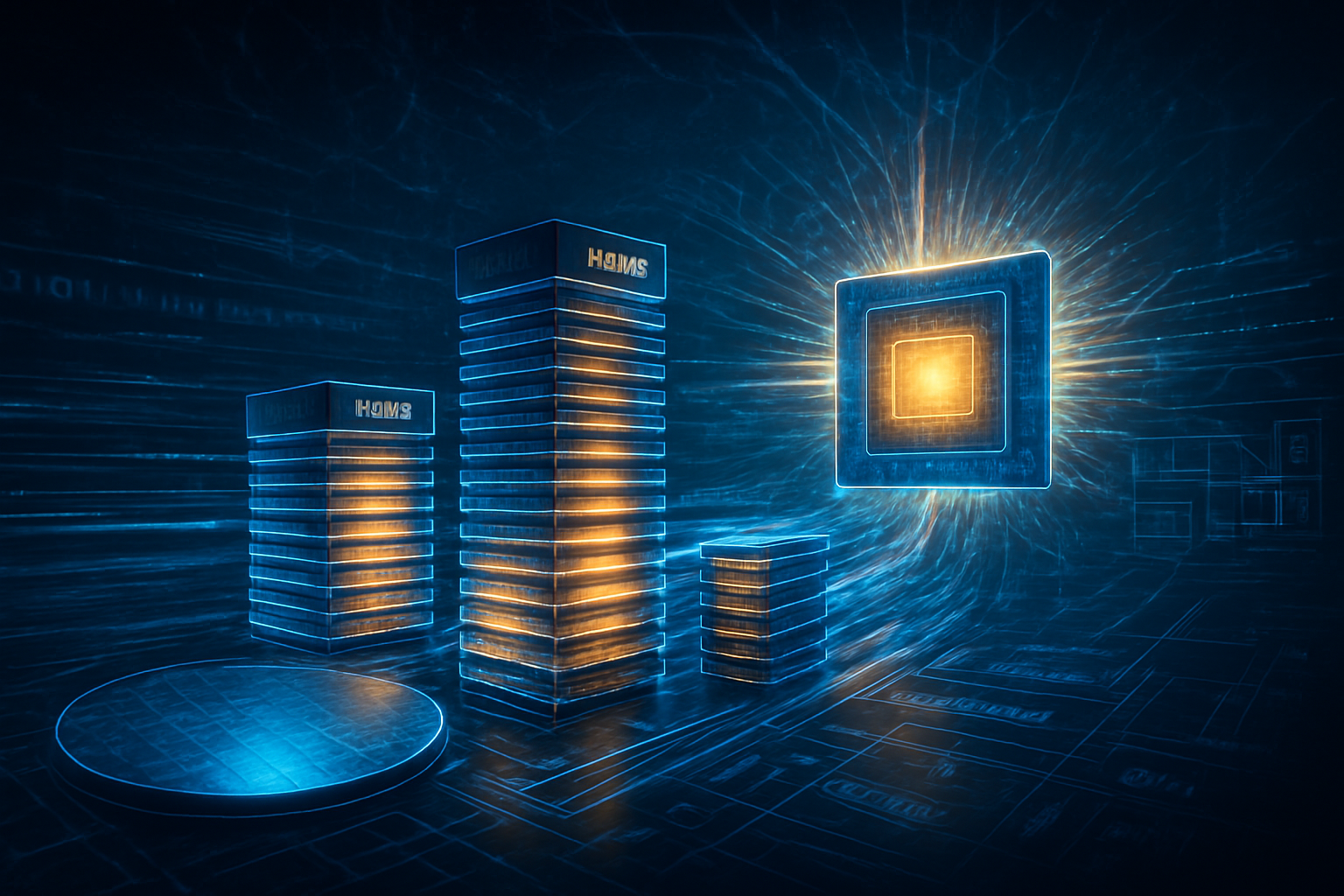
The Rubin Architecture: A 22 TB/s Leap into Agentic AI
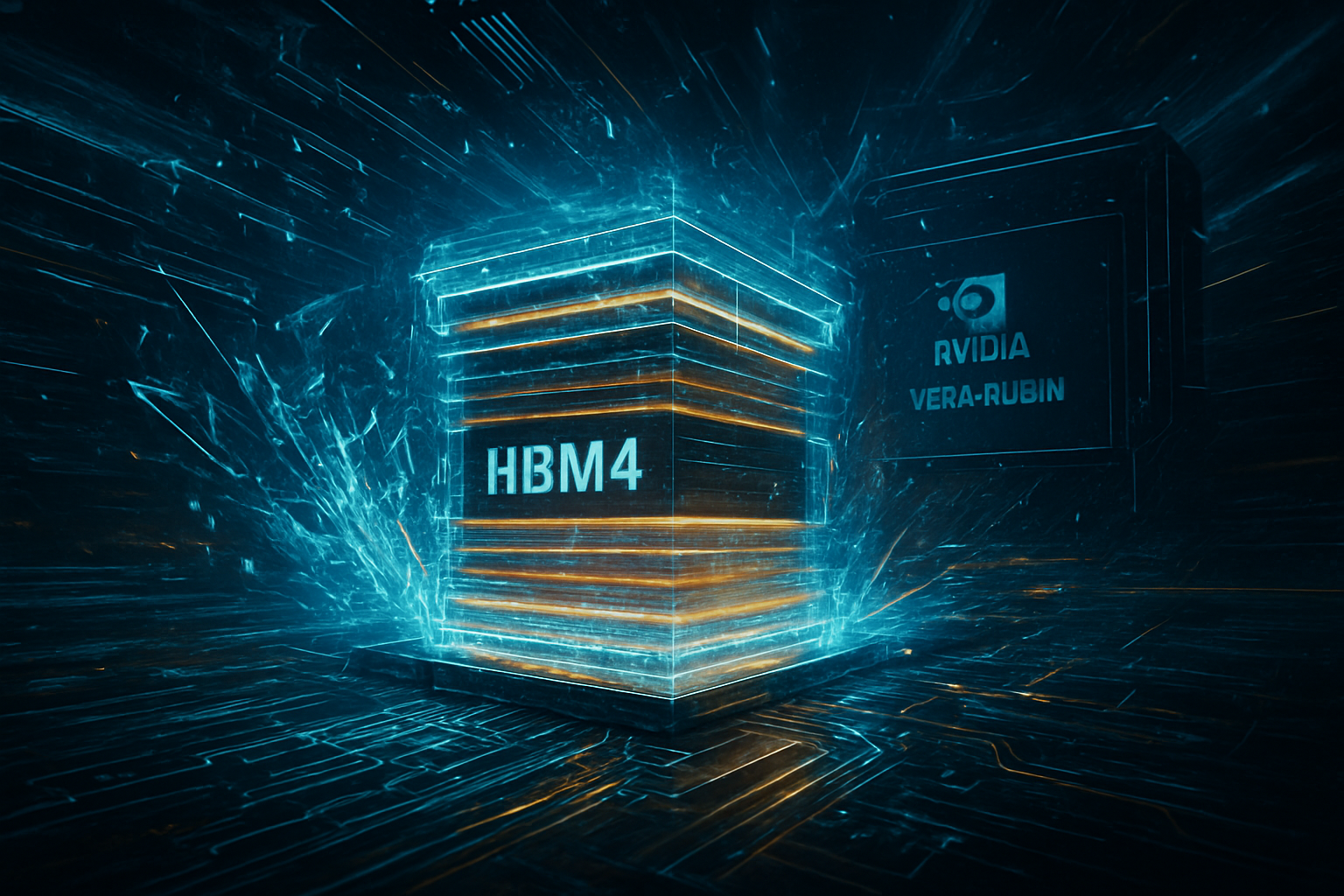
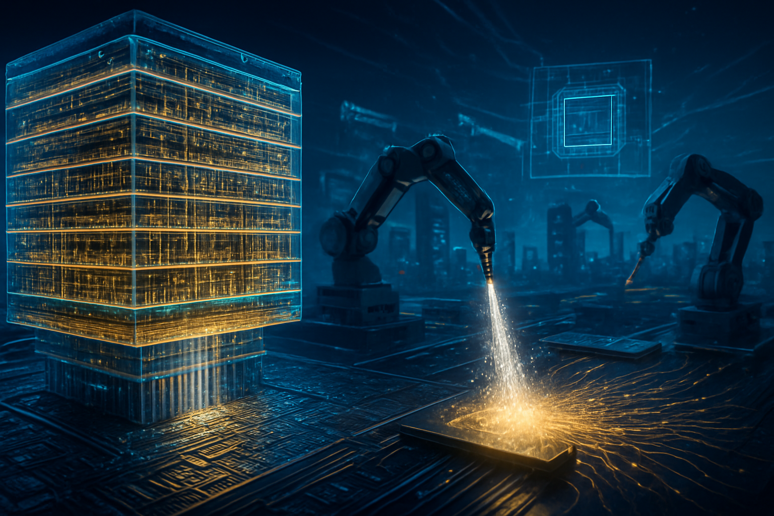
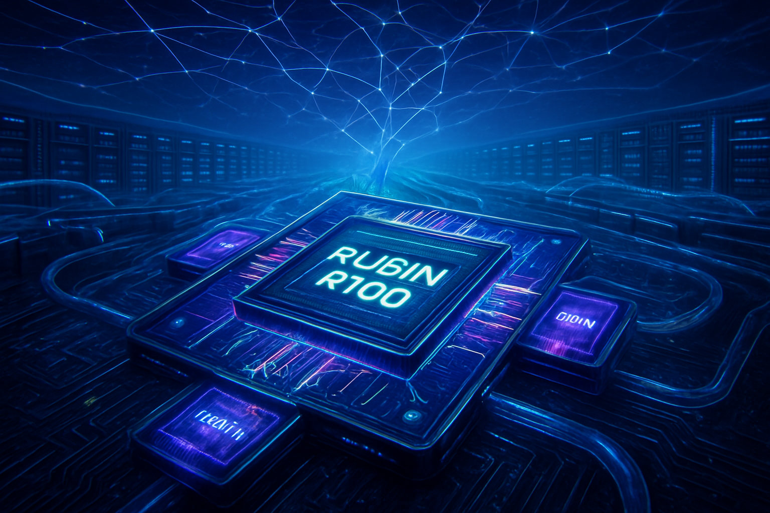
Unveiled at CES 2026, NVIDIA (NASDAQ:NVDA) has set a new high-water mark with the Rubin (R100) architecture. Built on an enhanced 3nm process from Taiwan Semiconductor Manufacturing Company (NYSE:TSM), Rubin moves away from the monolithic designs of the past toward a sophisticated chiplet-based approach. The headline specification is the integration of HBM4 memory, providing a staggering 22 TB/s of memory bandwidth. This is a 2.8x increase over the Blackwell Ultra architecture of 2025, effectively shattering the "memory wall" that has long throttled the performance of large language models (LLMs).
Accompanying the R100 GPU is the new Vera CPU, the successor to the Grace CPU. The "Vera Rubin" superchip is specifically optimized for what industry experts call "Agentic AI"—autonomous systems that require high-speed reasoning, planning, and long-term memory. Unlike previous iterations that focused primarily on raw throughput, the Rubin platform is designed for low-latency inference and complex multi-step orchestration. Initial reactions from the research community suggest that Rubin could reduce the time-to-train for 100-trillion parameter models from months to weeks, a feat previously thought impossible before the end of the decade.
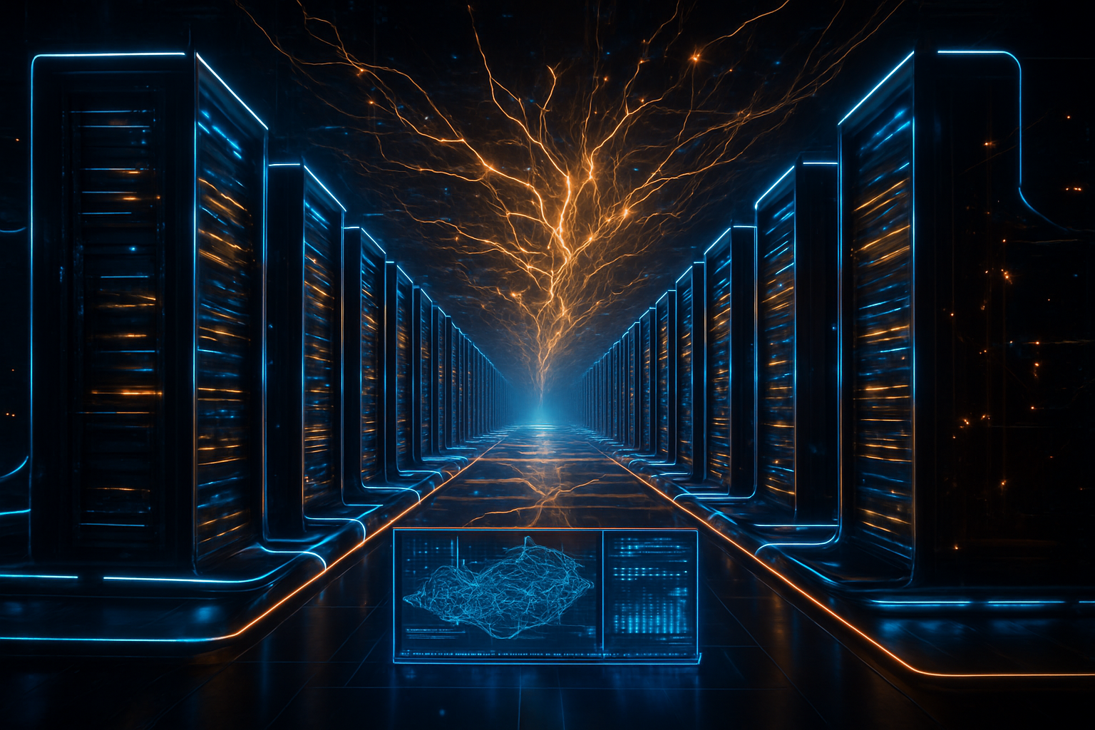
The Rise of the Superfactory: Microsoft’s 'Fairwater' Initiative
While NVIDIA provides the brains, Microsoft (NASDAQ:MSFT) is building the body. Project "Fairwater" represents a radical departure from traditional data center design. Rather than building isolated facilities, Microsoft is constructing "planet-scale AI superfactories" in locations like Mount Pleasant, Wisconsin, and Atlanta, Georgia. These sites are linked by a dedicated AI Wide Area Network (AI-WAN) backbone, a private fiber-optic mesh that allows data centers hundreds of miles apart to function as a single, unified supercomputer.
This infrastructure is purpose-built for the Rubin era. Fairwater facilities feature a vertical rack layout designed to support the extreme power and cooling requirements of NVIDIA’s GB300 and Rubin systems. To handle the heat generated by 4-Exaflop racks, Microsoft has deployed the world’s largest closed-loop liquid cooling system, which recycles water with near-zero consumption. By treating the entire "superfactory" as a single machine, Microsoft can train next-generation frontier models for OpenAI with unprecedented efficiency, positioning itself as the undisputed leader in AI infrastructure.
Eliminating the Bottleneck: Custom ARM CPUs for the GPU Age
The biggest challenge in the Rubin era is no longer the GPU itself, but the "CPU bottleneck"—the inability of traditional processors to feed data to GPUs fast enough. To solve this, Amazon (NASDAQ:AMZN), Alphabet (NASDAQ:GOOGL), and Meta Platforms (NASDAQ:META) have all doubled down on custom ARM-based silicon. Amazon’s Graviton5, launched in late 2025, features 192 cores and a revolutionary "NVLink Fusion" technology. This allows the Graviton5 to communicate directly with NVIDIA GPUs over a unified high-speed fabric, reducing communication latency by over 30%.
Google has taken a similar path with its Axion CPU, integrated into its "AI Hypercomputer" architecture. Axion uses custom "Titanium" offload controllers to manage the massive networking and I/O demands of Rubin pods, ensuring that the GPUs are never idle. Meanwhile, Meta has pivoted to a "customizable base" strategy with Arm Holdings (NASDAQ:ARM), optimizing the PyTorch library to run natively on their internal silicon and NVIDIA’s Grace-Rubin superchips. These custom CPUs are not meant to replace NVIDIA GPUs, but to act as the perfect "waiter," ensuring the GPU "chef" is always supplied with the data it needs to cook.
The Wider Significance: Sovereign AI and the Efficiency Mandate
The shift toward custom hyperscaler silicon and superfactories marks a turning point in the global AI landscape. We are moving away from a world where AI is a software layer on top of general hardware, and toward a world of "Sovereign AI" infrastructure. For tech giants, the ability to design their own silicon provides a massive strategic advantage: they can optimize for their specific workloads—be it search, social media ranking, or enterprise productivity—while reducing their reliance on external vendors and lowering their long-term capital expenditures.
However, this trend also raises concerns about the "compute divide." The sheer scale of projects like Fairwater suggests that only the wealthiest nations and corporations will be able to afford the infrastructure required to train the next generation of AI. Comparisons are already being made to the Manhattan Project or the Space Race. Just as those milestones defined the 20th century, the construction of these AI superfactories will likely define the geopolitical and economic landscape of the mid-21st century, with energy efficiency and silicon sovereignty becoming the new metrics of national power.
Future Horizons: From Rubin to Vera and Beyond
Looking ahead, the industry is already whispering about what comes after Rubin. NVIDIA’s annual cadence suggests that a successor—potentially codenamed "Vera" or another astronomical pioneer—is already in the simulation phase for a 2027 release. Experts predict that the next major breakthrough will involve optical interconnects, replacing copper wiring within the rack to further reduce power consumption and increase data speeds. As AI agents become more autonomous, the demand for "on-the-fly" model retraining will grow, requiring even tighter integration between custom cloud silicon and GPU clusters.
The challenges remain formidable. Powering these superfactories will require a massive expansion of the electrical grid and potentially the deployment of small modular reactors (SMRs) directly on-site. Furthermore, as the software stack becomes increasingly specialized for custom silicon, the industry must ensure that open-source frameworks remain compatible across different hardware ecosystems to prevent vendor lock-in. The coming months will be critical as the first Rubin-based systems begin their initial test runs in the Fairwater superfactories.
A New Chapter in Computing History
The emergence of custom hyperscaler silicon in the Rubin era represents the most significant architectural shift in computing since the transition from mainframes to the client-server model. By co-designing the CPU, the GPU, and the physical data center itself, companies like Microsoft, AWS, and Google are creating a foundation for AI that was previously the stuff of science fiction. The "Fairwater" project and the new generation of ARM CPUs are not just incremental improvements; they are the blueprints for the future of intelligence.
As we move through 2026, the industry will be watching closely to see how these massive investments translate into real-world AI capabilities. The key takeaways are clear: the era of general-purpose compute is over, the era of the AI superfactory has begun, and the race for silicon sovereignty is just heating up. For enterprises and developers, the message is simple: the tools of the trade are changing, and those who can best leverage this new, vertically integrated stack will be the ones who define the next decade of innovation.
This content is intended for informational purposes only and represents analysis of current AI developments.
TokenRing AI delivers enterprise-grade solutions for multi-agent AI workflow orchestration, AI-powered development tools, and seamless remote collaboration platforms.
For more information, visit https://www.tokenring.ai/.