Tag: Nvidia

  • Micron Secures AI Future with $1.8 Billion Acquisition of PSMC’s P5 Fab in Taiwan

    Micron Secures AI Future with $1.8 Billion Acquisition of PSMC’s P5 Fab in Taiwan

    In a bold move to cement its position in the high-stakes artificial intelligence hardware race, Micron Technology (NASDAQ: MU) has announced a definitive agreement to acquire the P5 fabrication facility in Tongluo, Taiwan, from Powerchip Semiconductor Manufacturing Corp (TWSE: 6770) for $1.8 billion. This strategic acquisition, finalized in January 2026, is designed to drastically scale Micron’s production of High Bandwidth Memory (HBM), the critical specialized DRAM that powers the world’s most advanced AI accelerators and large language model (LLM) clusters.

    The deal marks a pivotal shift for Micron as it transitions from a capacity-constrained challenger to a primary architect of the global AI supply chain. With the demand for HBM3E and the upcoming HBM4 standards reaching unprecedented levels, the acquisition of the 300,000-square-foot P5 cleanroom provides Micron with the immediate industrial footprint necessary to bypass the years-long lead times associated with greenfield factory construction. As the AI "supercycle" continues to accelerate, this $1.8 billion investment represents a foundational pillar in Micron’s quest to capture 25% of the HBM market share by the end of the year.

    The Technical Edge: Solving the "Wafer Penalty"

    The technical implications of the P5 acquisition center on the "wafer penalty" inherent to HBM production. Unlike standard DDR5 memory, HBM dies are significantly larger and require a more complex, multi-layered stacking process using Through-Silicon Vias (TSV). This architectural complexity means that producing HBM requires roughly three times the wafer capacity of traditional DRAM to achieve the same bit output. By taking over the P5 site—a facility that PSMC originally invested over $9 billion to develop—Micron gains a massive, ready-made environment to house its advanced "1-gamma" and "1-delta" manufacturing nodes.

    The P5 facility is expected to be integrated into Micron’s existing Taiwan-based production cluster, which already includes its massive Taichung "megafab." This proximity allows for a streamlined logistics chain for the delicate HBM stacking process. While the transaction is expected to close in the second quarter of 2026, Micron is already planning to retool the facility for HBM4 production. HBM4, the next generational leap in memory technology, is projected to offer a 60% increase in bandwidth over current HBM3E standards and will utilize 2048-bit interfaces, necessitating the ultra-precise lithography and cleanroom standards that the P5 fab provides.

    Initial reactions from the industry have been overwhelmingly positive, with analysts noting that the $1.8 billion price tag is exceptionally capital-efficient. Industry experts at TrendForce have pointed out that acquiring a "brownfield" site—an existing, modern facility—allows Micron to begin meaningful wafer output by the second half of 2027. This is significantly faster than the five-to-seven-year timeline required to build its planned $100 billion mega-site in New York from the ground up. Researchers within the semiconductor space view this as a necessary survival tactic in an era where HBM supply for 2026 is already reported as "sold out" across the entire industry.

    Market Disruptions: Chasing the HBM Crown

    The acquisition fundamentally redraws the competitive map for the memory industry, where Micron has historically trailed South Korean giants SK Hynix (KRX: 000660) and Samsung Electronics (KRX: 005930). Throughout 2024 and 2025, SK Hynix maintained a dominant lead, controlling nearly 57% of the HBM market due to its early and exclusive supply deals with NVIDIA (NASDAQ: NVDA). However, Micron’s aggressive expansion in Taiwan, which includes the 2024 purchase of AU Optronics (TWSE: 2409) facilities for advanced packaging, has seen its market share surge from a mere 5% to over 21% in just two years.

    For tech giants like NVIDIA and Advanced Micro Devices (NASDAQ: AMD), Micron’s increased capacity is a welcome development that may ease the chronic supply shortages of AI GPUs like the Blackwell B200 and the upcoming Vera Rubin architectures. By diversifying the HBM supply chain, these companies gain more leverage in pricing and reduce their reliance on a single geographic or corporate source. Conversely, for Samsung, which has struggled with yield issues on its 12-high HBM3E stacks, Micron’s rapid scaling represents a direct threat to its traditional second-place standing in the global memory rankings.

    The strategic advantage for Micron lies in its localized ecosystem in Taiwan. By centering its HBM production in the same geographic region as Taiwan Semiconductor Manufacturing Company (NYSE: TSM), the world’s leading chip foundry, Micron can more efficiently collaborate on CoWoS (Chip on Wafer on Substrate) packaging. This integration is vital because HBM is not a standalone component; it must be physically bonded to the AI processor. Micron’s move to own the manufacturing floor rather than leasing capacity ensures that it can maintain strict quality control and proprietary manufacturing techniques that are essential for the high-yield production of 12-layer and 16-layer HBM stacks.

    The Global AI Landscape: From Code to Carbon

    Looking at the broader AI landscape, the Micron-PSMC deal is a clear indicator that the "AI arms race" has moved from the software layer to the physical infrastructure layer. In the early 2020s, the focus was on model parameters and training algorithms; in 2026, the bottleneck is physical cleanroom space and the availability of high-purity silicon wafers. The acquisition fits into a larger trend of "reshoring" and "near-shoring" within the semiconductor industry, where proximity to downstream partners like TSMC and Foxconn (TWSE: 2317) is becoming a primary competitive advantage.

    However, this consolidation of manufacturing power is not without its concerns. The heavy concentration of HBM production in Taiwan continues to pose a geopolitical risk, as any regional instability could theoretically halt the global supply of AI-capable hardware. Furthermore, the sheer capital intensity required to compete in the HBM market is creating a "winner-take-all" dynamic. With Micron spending billions to secure capacity that is already sold out years in advance, smaller memory manufacturers are being effectively locked out of the most profitable segment of the industry, potentially stifling innovation in alternative memory architectures.

    In terms of historical milestones, this acquisition echoes the massive capital expenditures seen during the height of the mobile smartphone boom in the early 2010s, but on a significantly larger scale. The HBM market is no longer a niche segment of the DRAM industry; it is the primary engine of growth. Micron’s transformation into an AI-first company is now complete, as the company reallocates nearly all of its advanced research and development and capital expenditure toward supporting the demands of hyperscale data centers and generative AI workloads.

    Future Horizons: The Road to HBM4 and PIM

    In the near term, the industry will be watching for the successful closure of the deal in Q2 2026 and the subsequent retooling of the P5 facility. The next major milestone will be the transition to HBM4, which is expected to enter high-volume production later this year. This new standard will move the base logic die of the HBM stack from a memory process to a foundry process, requiring even closer collaboration between Micron and TSMC. If Micron can successfully navigate this technical transition while scaling the P5 fab, it could potentially overtake Samsung to become the world’s second-largest HBM supplier by 2027.

    Beyond the immediate horizon, the P5 fab may also serve as a testing ground for experimental technologies like HBM4E and the integration of optical interconnects directly into the memory stack. As AI models continue to grow in size, the "memory wall"—the gap between processor speed and memory bandwidth—remains the greatest challenge for the industry. Experts predict that the next decade of AI development will be defined by "processing-in-memory" (PIM) architectures, where the memory itself performs basic computational tasks. The vast cleanroom space of the P5 fab provides Micron with the playground necessary to develop these next-generation hybrid chips.

    Conclusion: A Definitive Stake in the AI Era

    The acquisition of the P5 fab for $1.8 billion is more than a simple real estate transaction; it is a declaration of intent by Micron Technology. By securing one of the most modern fabrication sites in Taiwan, Micron has effectively bought its way to the front of the AI hardware revolution. The deal addresses the critical need for wafer capacity, positions the company at the heart of the world’s most advanced semiconductor ecosystem, and provides a clear roadmap for the rollout of HBM4 and beyond.

    As the transaction moves toward its close in the coming months, the key takeaways are clear: the AI supercycle shows no signs of slowing down, and the battle for dominance is being fought in the cleanrooms of Taiwan. For investors and industry watchers, the focus will now shift to Micron’s ability to execute on its aggressive production targets and its capacity to maintain yields as HBM stacks become increasingly complex. In the historical narrative of artificial intelligence, the January 2026 acquisition of the P5 fab may well be remembered as the moment Micron secured its seat at the table of the AI elite.


    This content is intended for informational purposes only and represents analysis of current AI developments.

    TokenRing AI delivers enterprise-grade solutions for multi-agent AI workflow orchestration, AI-powered development tools, and seamless remote collaboration platforms.
    For more information, visit https://www.tokenring.ai/.

  • The Dawn of the Physical AI Era: Silicon Titans Redefine CES 2026

    The Dawn of the Physical AI Era: Silicon Titans Redefine CES 2026

    The recently concluded CES 2026 in Las Vegas will be remembered as the moment the artificial intelligence revolution stepped out of the chat box and into the physical world. Officially heralded as the "Year of Physical AI," the event marked a historic pivot from the generative text and image models of 2024–2025 toward embodied systems that can perceive, reason, and act within our three-dimensional environment. This shift was underscored by a massive coordinated push from the world’s leading semiconductor manufacturers, who unveiled a new generation of "Physical AI" processors designed to power everything from "Agentic PCs" to fully autonomous humanoid robots.

    The significance of this year’s show lies in the maturation of edge computing. For the first time, the industry demonstrated that the massive compute power required for complex reasoning no longer needs to reside exclusively in the cloud. With the launch of ultra-high-performance NPUs (Neural Processing Units) from the industry's "Four Horsemen"—Nvidia, Intel, AMD, and Qualcomm—the promise of low-latency, private, and physically capable AI has finally moved from research prototypes to mass-market production.

    The Silicon War: Specs of the 'Four Horsemen'

    The technological centerpiece of CES 2026 was the "four-way war" in AI silicon. Nvidia (NASDAQ:NVDA) set the pace early by putting its "Rubin" architecture into full production. CEO Jensen Huang declared a "ChatGPT moment for robotics" as he unveiled the Jetson T4000, a Blackwell-powered module delivering a staggering 1,200 FP4 TFLOPS. This processor is specifically designed to be the "brain" of humanoid robots, supported by Project GR00T and Cosmos, an "open world foundation model" that allows machines to learn motor tasks from video data rather than manual programming.

    Not to be outdone, Intel (NASDAQ:INTC) utilized the event to showcase the success of its turnaround strategy with the official launch of Panther Lake (Core Ultra Series 3). Manufactured on the cutting-edge Intel 18A process node, the chip features the new NPU 5, which delivers 50 TOPS locally. Intel’s focus is the "Agentic AI PC"—a machine capable of managing a user’s entire digital life and local file processing autonomously. Meanwhile, Qualcomm (NASDAQ:QCOM) flexed its efficiency muscles with the Snapdragon X2 Elite Extreme, boasting an 18-core Oryon 3 CPU and an 80 TOPS NPU. Qualcomm also introduced the Dragonwing IQ10, a dedicated platform for robotics that emphasizes power-per-watt, enabling longer battery life for mobile humanoids like the Vinmotion Motion 2.

    AMD (NASDAQ:AMD) rounded out the quartet by bridging the gap between the data center and the desktop. Their new Ryzen AI "Gorgon Point" series features an expanded matrix engine and the first native support for "Copilot+ Desktop" high-performance workloads. AMD also teased its Helios platform, a rack-scale solution powered by Zen 6 EPYC "Venice" processors, intended to train the very physical world models that the smaller Ryzen chips execute at the edge. Industry experts have noted that while previous years focused on software breakthroughs, 2026 is defined by the hardware's ability to handle "multimodal reasoning"—the ability for a device to see an object, understand its physical properties, and decide how to interact with it in real-time.

    Market Maneuvers: From Cloud Dominance to Edge Supremacy

    This shift toward Physical AI is fundamentally reshaping the competitive landscape of the tech industry. For years, the AI narrative was dominated by cloud providers and LLM developers. However, CES 2026 proved that the "edge"—the devices we carry and the robots that work alongside us—is the new battleground for strategic advantage. Nvidia is positioning itself as the "Infrastructure King," providing not just the chips but the entire software stack (Omniverse and Isaac) needed to simulate and train physical entities. By owning the simulation environment, Nvidia seeks to make its hardware the indispensable foundation for every robotics startup.

    In contrast, Qualcomm and Intel are targeting the "volume market." Qualcomm is leveraging its heritage in mobile connectivity to dominate "connected robotics," where 5G and 6G integration are vital for warehouse automation and consumer bots. Intel, through its 18A manufacturing breakthrough, is attempting to reclaim the crown of the "PC Brain" by making AI features so deeply integrated into the OS that a cloud connection becomes optional. Startups like Boston Dynamics (backed by Hyundai and Google DeepMind) and Vinmotion are the primary beneficiaries of this rivalry, as the sudden abundance of high-performance, low-power silicon allows them to transition from experimental models to production-ready units capable of "human-level" dexterity.

    The competitive implications extend beyond silicon. Tech giants are now forced to choose between "walled garden" AI ecosystems or open-source Physical AI frameworks. The move toward local processing also threatens the dominance of current subscription-based AI models; if a user’s Intel-powered laptop or Qualcomm-powered robot can perform complex reasoning locally, the strategic advantage of centralized AI labs like OpenAI or Anthropic could begin to erode in favor of hardware-software integrated giants.

    The Wider Significance: When AI Gets a Body

    The transition from "Digital AI" to "Physical AI" represents a profound milestone in human-computer interaction. For the first time, the "hallucinations" that plagued early generative AI have moved from being a nuisance in text to a safety critical engineering challenge. At CES 2026, panels featuring leaders from Siemens and Mercedes-Benz emphasized that "Physical AI" requires "error intolerance." A robot navigating a crowded home or a factory floor cannot afford a single reasoning error, leading to the introduction of "safety-grade" silicon architectures that partition AI logic from critical motor controls.

    This development also brings significant societal concerns to the forefront. As AI becomes embedded in physical infrastructure—from elevators that predict maintenance to autonomous industrial helpers—the question of accountability becomes paramount. Experts at the event raised alarms regarding "invisible AI," where autonomous systems become so pervasive that their decision-making processes are no longer transparent to the humans they serve. The industry is currently racing to establish "document trails" for AI reasoning to ensure that when a physical system fails, the cause can be diagnosed with the same precision as a mechanical failure.

    Comparatively, the 2023 generative AI boom was about "creation," while the 2026 Physical AI breakthrough is about "utility." We are moving away from AI as a toy or a creative partner and toward AI as a functional laborer. This has reignited debates over labor displacement, but with a new twist: the focus is no longer just on white-collar "knowledge work," but on blue-collar tasks in logistics, manufacturing, and elder care.

    Beyond the Horizon: The 2027 Roadmap

    Looking ahead, the momentum generated at CES 2026 shows no signs of slowing. Near-term developments will likely focus on the refinement of "Agentic AI PCs," where the operating system itself becomes a proactive assistant that performs tasks across different applications without user prompting. Long-term, the industry is already looking toward 2027, with Intel teasing its Nova Lake architecture (rumored to feature 52 cores) and AMD preparing its Medusa (Zen 6) chips based on TSMC’s 2nm process. These upcoming iterations aim to bring even more "brain-like" density to consumer hardware.

    The next major challenge for the industry will be the "sim-to-real" gap—the difficulty of taking an AI trained in a virtual simulation and making it function perfectly in the messy, unpredictable real world. Future applications on the horizon include "personalized robotics," where robots are not just general-purpose tools but are fine-tuned to the specific layout and needs of an individual's home. Predictably, experts believe the next 18 months will see a surge in M&A activity as silicon giants move to acquire robotics software startups to complete their "Physical AI" portfolios.

    The Wrap-Up: A Turning Point in Computing History

    CES 2026 has served as a definitive declaration that the "post-chat" era of artificial intelligence has arrived. The key takeaways from the event are clear: the hardware has finally caught up to the software, and the focus of innovation has shifted from virtual outputs to physical actions. The coordinated launches from Nvidia, Intel, AMD, and Qualcomm have provided the foundation for a world where AI is no longer a guest on our screens but a participant in our physical spaces.

    In the history of AI, 2026 will likely be viewed as the year the technology gained its "body." As we look toward the coming months, the industry will be watching closely to see how these new processors perform in real-world deployments and how consumers react to the first wave of truly autonomous "Agentic" devices. The silicon war is far from over, but the battlefield has officially moved into the real world.


    This content is intended for informational purposes only and represents analysis of current AI developments.

    TokenRing AI delivers enterprise-grade solutions for multi-agent AI workflow orchestration, AI-powered development tools, and seamless remote collaboration platforms.
    For more information, visit https://www.tokenring.ai/.

  • The Silicon Iron Curtain: How ‘Pax Silica’ and New Trade Taxes are Redrawing the AI Frontier

    The Silicon Iron Curtain: How ‘Pax Silica’ and New Trade Taxes are Redrawing the AI Frontier

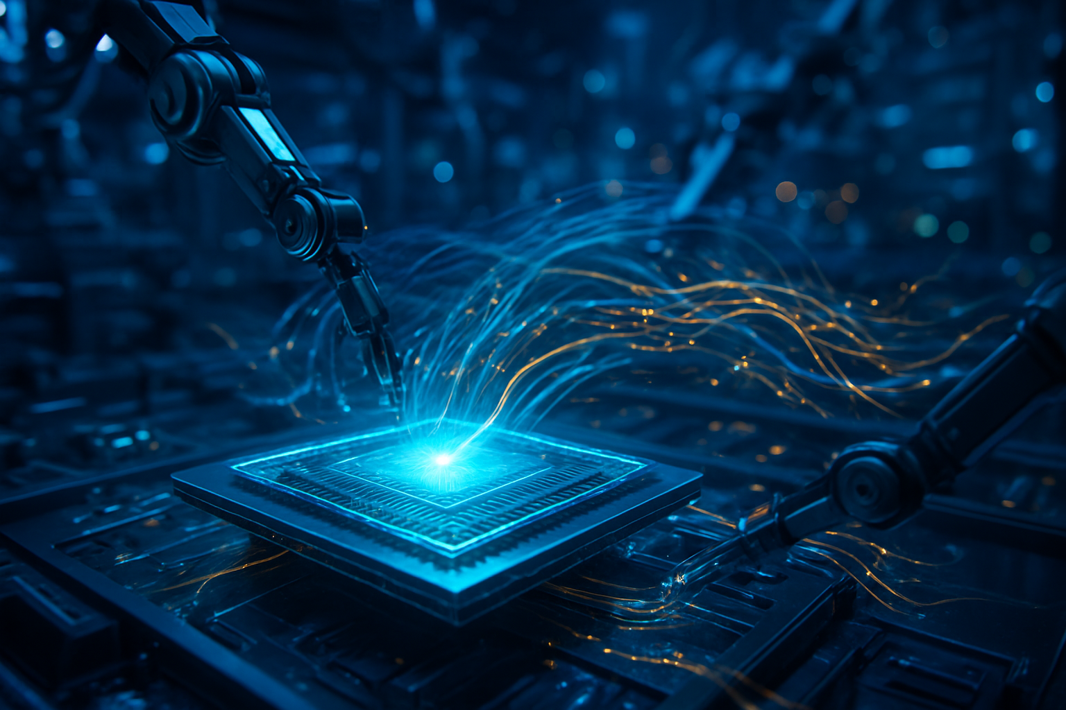
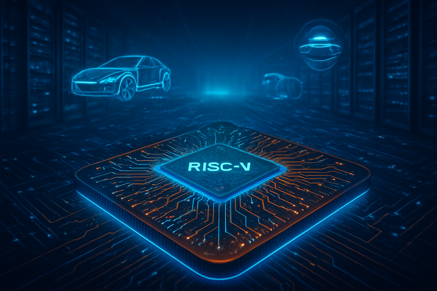
    As of January 2026, the global semiconductor landscape has undergone a seismic shift, moving away from the era of "containment" toward a complex new reality of "monetized competition." The geopolitical tug-of-war between the United States and China has solidified into a permanent bifurcation of the technology world, marked by the formalization of the "Pax Silica" alliance—the strategic successor to the "Chip 4" coalition. This new diplomatic framework, which now includes the original Chip 4 nations plus the Netherlands, Singapore, and recent additions like the UAE and Qatar, seeks to insulate the most advanced AI hardware from geopolitical rivals while maintaining a controlled, heavily taxed economic bridge to the East.

    The immediate significance of this development cannot be overstated: the U.S. Department of Commerce has officially pivoted from a blanket "presumption of denial" for high-end chip exports to a "case-by-case review" system paired with a mandatory 25% "chip tax" on all advanced AI silicon bound for China. This policy allows Western titans like NVIDIA (NASDAQ:NVDA) to maintain market share while simultaneously generating billions in revenue for the U.S. government to reinvest in domestic sub-2nm fabrication and research. However, this bridge comes with strings attached, as the most cutting-edge "sovereign-grade" AI architectures remain strictly off-limits to any nation outside the Pax Silica security umbrella.

    The Architecture of Exclusion: GAA Transistors and HBM Chokepoints

    Technically, the new trade restrictions center on two critical pillars of next-generation computing: Gate-All-Around (GAA) transistor technology and High Bandwidth Memory (HBM). While the previous decade was defined by FinFET transistors, the leap to 2nm and 3nm nodes requires the adoption of GAA, which allows for finer control over current and significantly lower power consumption—essential for the massive energy demands of 2026-era Large Action Models (LAMs). New export rules, specifically ECCN 3A090.c, now strictly control the software, recipes, and hybrid bonding tools required to manufacture GAA-based chips, effectively stalling China’s progress at the 5nm ceiling.

    In the memory sector, HBM has become the "new oil" of the AI industry. The Pax Silica alliance has placed a firm stranglehold on the specialized stacking and bonding equipment required to produce HBM4, the current industry standard. This has forced Chinese firms like SMIC (HKG:0981) to attempt to localize the entire HBM supply chain—a monumental task that experts suggest is at least three to five years behind the state-of-the-art. Industry analysts note that while SMIC has managed to produce 5nm-class chips using older Deep Ultraviolet (DUV) lithography, their yields are reportedly hovering around a disastrous 33%, making their domestic AI accelerators nearly twice as expensive as their Western counterparts.

    Initial reactions from the AI research community have been polarized. While some argue that these restrictions prevent the proliferation of dual-use AI for military applications, others fear a "hardware apartheid" that could slow global scientific progress. The shift by ASML (NASDAQ:ASML) to fully align with U.S. policy, halting the export of even high-end immersion DUV tools to China, has further tightened the noose, forcing Chinese researchers to focus on algorithmic efficiency and "compute-light" AI models to compensate for their lack of raw hardware power.

    A Two-Tiered Market: Winners and Losers in the New Trade Regime

    For the corporate giants of Silicon Valley and East Asia, 2026 is a year of navigating "dual-track" product lines. NVIDIA (NASDAQ:NVDA) recently unveiled its "Rubin" platform, a successor to the Blackwell architecture featuring Vera CPUs. Crucially, the Rubin platform is classified as "Pax Silica Only," meaning it cannot be exported to China even with the 25% tax. Instead, NVIDIA is shipping the older H200 and specialized "H20" variants to the Chinese market, subject to a volume cap that prevents China-bound shipments from exceeding 50% of U.S. domestic sales. This strategy allows NVIDIA to keep its dominant position in the Chinese enterprise market while ensuring the U.S. maintains a "two-generation lead."

    The strategic positioning of TSMC (NYSE:TSM) has also evolved. Through a landmark $250 billion "Silicon Shield" agreement finalized in early 2026, TSMC has secured massive federal subsidies for its Arizona and Dresden facilities in exchange for prioritizing Pax Silica defense and AI infrastructure needs. This has mitigated fears of a "hollowing out" of Taiwan’s industrial base, as the island remains the exclusive home for the initial "N2" (2nm) mass production. Meanwhile, South Korean giants Samsung (KRX:005930) and SK Hynix (KRX:000660) are reaping the benefits of the HBM shortage, though they face the difficult task of phasing out their legacy manufacturing footprints in mainland China to comply with the new alliance standards.

    Startups in the AI space are feeling the squeeze of this bifurcation. New ventures in India and Singapore are benefiting from being inside the Pax Silica "trusted circle," gaining access to advanced compute that was previously reserved for U.S. and European firms. Conversely, Chinese AI startups are pivoting toward RISC-V architectures and domestic accelerators, creating a siloed ecosystem that is increasingly incompatible with Western software stacks like CUDA, potentially leading to a permanent divergence in AI development environments.

    The Geopolitical Gamble: Sovereignty vs. Globalization

    The wider significance of these trade restrictions marks the end of the "Global Village" era for high-technology. We are witnessing the birth of "Semiconductor Sovereignty," where the ability to design and manufacture silicon is viewed as being as vital to national security as a nuclear deterrent. This fits into a broader trend of "de-risking" rather than "de-coupling," where the U.S. and its allies seek to control the heights of the AI revolution while maintaining enough trade to prevent a total economic collapse.

    The Pax Silica alliance represents a sophisticated evolution of the Cold War-era COCOM (Coordinating Committee for Multilateral Export Controls). By including energy-rich nations like the UAE and Qatar, the U.S. is effectively trading access to high-end AI chips for long-term energy security and a commitment to Western data standards. However, this creates a potential "splinternet" of hardware, where the world is divided into those who can run 2026’s most advanced models and those who are stuck with the "legacy" AI of 2024.

    Comparisons to previous milestones, such as the 1986 U.S.-Japan Semiconductor Agreement, highlight the increased stakes. In the 1980s, the battle was over memory chips for PCs; today, it is over the foundational "intelligence" that will power autonomous economies, defense systems, and scientific discovery. The concern remains that by pushing China into a corner, the West is incentivizing a radical, independent breakthrough in areas like optical computing or carbon nanotube transistors—technologies that could eventually bypass the silicon-based chokepoints currently being exploited.

    The Horizon: Photonics, RISC-V, and the 2028 Deadline

    Looking ahead, the next 24 months will be a race against time. China has set a national goal for 2028 to achieve "EUV-equivalence" through alternative lithography techniques and advanced chiplet packaging. While Western experts remain skeptical, the massive influx of capital into China’s "Big Fund Phase 3" is accelerating the localization of ion implanters and etching equipment. We can expect to see the first "all-Chinese" 7nm AI chips hitting the market by late 2026, though their performance per watt will likely lag behind the West’s 2nm offerings.

    In the near term, the industry is closely watching the development of silicon photonics. This technology, which uses light instead of electricity to move data between chips, could be the key to overcoming the interconnect bottlenecks that currently plague AI clusters. Because photonics relies on different manufacturing processes than traditional logic chips, it could become a new "gray zone" for trade restrictions, as the Pax Silica framework struggles to categorize these hybrid devices.

    The long-term challenge will be the "talent drain." As the hardware divide grows, we may see a migration of researchers toward whichever ecosystem provides the best "compute-to-cost" ratio. If China can subsidize its inefficient 5nm chips enough to make them accessible to global researchers, it could create a gravity well for AI development that rivals the Western hubs, despite the technical inferiority of the underlying hardware.

    A New Equilibrium in the AI Era

    The geopolitical hardening of the semiconductor supply chain in early 2026 represents a definitive closing of the frontier. The transition from the "Chip 4" to "Pax Silica" and the implementation of the 25% "chip tax" signals that the U.S. has accepted the permanence of its rivalry with China and has moved to monetize it while protecting its technological lead. This development will be remembered as the moment the AI revolution was formally subsumed by the machinery of statecraft.

    Key takeaways for the coming months include the performance of NVIDIA's Rubin platform within the Pax Silica bloc and whether China can successfully scale its 5nm "inefficiency-node" production to meet domestic demand. The "Silicon Shield" around Taiwan appears stronger than ever, but the cost of that security is a more expensive, more fragmented global market.

    In the weeks ahead, watch for the first quarterly reports from ASML (NASDAQ:ASML) and TSMC (NYSE:TSM) to see the true impact of the Dutch export bans and the U.S. investment deals. As the "Silicon Iron Curtain" descends, the primary question remains: will this enforced lead protect Western interests, or will it merely accelerate the arrival of a competitor that the West no longer understands?


    This content is intended for informational purposes only and represents analysis of current AI developments.

    TokenRing AI delivers enterprise-grade solutions for multi-agent AI workflow orchestration, AI-powered development tools, and seamless remote collaboration platforms.
    For more information, visit https://www.tokenring.ai/.

  • The Silicon Supercycle: Semiconductor Industry Poised to Shatter $1 Trillion Milestone in 2026

    The Silicon Supercycle: Semiconductor Industry Poised to Shatter $1 Trillion Milestone in 2026

    As of January 21, 2026, the global semiconductor industry stands on the precipice of a historic achievement: the $1 trillion annual revenue milestone. Long predicted by analysts to occur at the end of the decade, this monumental valuation has been pulled forward by nearly four years due to a "Silicon Supercycle" fueled by the insatiable demand for generative AI infrastructure and the rapid evolution of High Bandwidth Memory (HBM).

    This acceleration marks a fundamental shift in the global economy, transitioning the semiconductor sector from a cyclical industry prone to "boom and bust" periods in PCs and smartphones into a structural growth engine for the artificial intelligence era. With the industry crossing the $975 billion mark at the close of 2025, current Q1 2026 data indicates that the trillion-dollar threshold will be breached by mid-year, driven by a new generation of AI accelerators and advanced memory architectures.

    The Technical Engine: HBM4 and the 2048-bit Breakthrough

    The primary technical catalyst for this growth is the desperate need to overcome the "Memory Wall"—the bottleneck where data processing speeds outpace the ability of memory to feed that data to the processor. In 2026, the transition from HBM3e to HBM4 has become the industry's most significant technical leap. Unlike previous iterations, HBM4 doubles the interface width from a 1024-bit bus to a 2048-bit bus, providing bandwidth exceeding 2.0 TB/s per stack. This allows the latest AI models, which now routinely exceed several trillion parameters, to operate with significantly reduced latency.

    Furthermore, the manufacturing of these memory stacks has fundamentally changed. For the first time, the "base logic die" at the bottom of the HBM stack is being manufactured on advanced logic nodes, such as the 5nm process from TSMC (NYSE: TSM), rather than traditional DRAM nodes. This hybrid approach allows for much higher efficiency and closer integration with GPUs. To manage the extreme heat generated by these 16-hi and 20-hi stacks, the industry has widely adopted "Hybrid Bonding" (copper-to-copper), which replaces traditional microbumps and allows for thinner, more thermally efficient chips.

    Initial reactions from the AI research community have been overwhelmingly positive, as these hardware gains are directly translating to a 3x to 5x improvement in training efficiency for next-generation large multimodal models (LMMs). Industry experts note that without the 2026 deployment of HBM4, the scaling laws of AI would have likely plateaued due to energy constraints and data transfer limitations.

    The Market Hierarchy: Nvidia and the Memory Triad

    The drive toward $1 trillion has reshaped the corporate leaderboard. Nvidia (NASDAQ: NVDA) continues its reign as the world’s most valuable semiconductor company, having become the first chip designer to surpass $125 billion in annual revenue. Their dominance is currently anchored by the Blackwell Ultra and the newly launched Rubin architecture, which utilizes advanced HBM4 modules to maintain a nearly 90% share of the AI data center market.

    In the memory sector, a fierce "triad" has emerged between SK Hynix (KRX: 000660), Samsung Electronics (KRX: 005930), and Micron Technology (NASDAQ: MU). SK Hynix currently maintains a slim lead in HBM market share, but Samsung has gained significant ground in early 2026 by leveraging its "turnkey" model—offering memory, foundry, and advanced packaging under one roof. Micron has successfully carved out a high-margin niche by focusing on power-efficient HBM3e for edge-AI devices, which are now beginning to see mass adoption in the enterprise laptop and smartphone markets.

    This shift has left legacy players like Intel (NASDAQ: INTC) in a challenging position, as they race to pivot their manufacturing capabilities toward the advanced packaging services (like CoWoS-equivalent technologies) that AI giants demand. The competitive landscape is no longer just about who has the fastest processor, but who can secure the most capacity on TSMC’s 2nm and 3nm production lines.

    The Wider Significance: A Structural Shift in Global Compute

    The significance of the $1 trillion milestone extends far beyond corporate balance sheets. It represents a paradigm shift where the "compute intensity" of the global economy has reached a tipping point. In previous decades, the semiconductor market was driven by consumer discretionary spending on gadgets; today, it is driven by sovereign AI initiatives and massive capital expenditure from "Hyperscalers" like Microsoft, Google, and Meta.

    However, this rapid growth has raised significant concerns regarding power consumption and supply chain fragility. The concentration of advanced manufacturing in East Asia remains a geopolitical flashpoint, even as the U.S. and Europe bring more "fab" capacity online via the CHIPS Act. Furthermore, the sheer energy required to run the HBM-heavy data centers needed for the $1 trillion market is forcing a secondary boom in power semiconductors and "green" data center infrastructure.

    Comparatively, this milestone is being viewed as the "Internet Moment" for hardware. Just as the build-out of fiber optic cables in the late 1990s laid the groundwork for the digital economy, the current build-out of AI infrastructure is seen as the foundational layer for the next fifty years of autonomous systems, drug discovery, and climate modeling.

    Future Horizons: Beyond HBM4 and Silicon Photonics

    Looking ahead to the remainder of 2026 and into 2027, the industry is already preparing for the next frontier: Silicon Photonics. As traditional electrical interconnects reach their physical limits, the industry is moving toward optical interconnects—using light instead of electricity to move data between chips. This transition is expected to further reduce power consumption and allow for even larger clusters of GPUs to act as a single, massive "super-chip."

    In the near term, we expect to see "Custom HBM" become the norm, where AI companies like OpenAI or Amazon design their own logic layers for memory stacks, tailored specifically to their proprietary algorithms. The challenge remains the yield rates of these incredibly complex 3D-stacked components; as chips become taller and more integrated, a single defect can render a very expensive component useless.

    The Road to $1 Trillion and Beyond

    The semiconductor industry's journey to $1 trillion in 2026 is a testament to the accelerating pace of human innovation. What was once a 2030 goal was reached four years early, catalyzed by the sudden and profound emergence of generative AI. The key takeaways from this milestone are clear: memory is now as vital as compute, advanced packaging is the new battlefield, and the semiconductor industry is now the undisputed backbone of global geopolitics and economics.

    As we move through 2026, the industry's focus will likely shift from pure capacity expansion to efficiency and sustainability. The "Silicon Supercycle" shows no signs of slowing down, but its long-term success will depend on how well the industry can manage the environmental and geopolitical pressures that come with being a trillion-dollar titan. In the coming months, keep a close eye on the rollout of Nvidia’s Rubin chips and the first shipments of mass-produced HBM4; these will be the bellwethers for the industry's next chapter.


    This content is intended for informational purposes only and represents analysis of current AI developments.

    TokenRing AI delivers enterprise-grade solutions for multi-agent AI workflow orchestration, AI-powered development tools, and seamless remote collaboration platforms.
    For more information, visit https://www.tokenring.ai/.

  • Silicon Sovereignty: TSMC Reaches 2nm Milestone and Triples Down on Arizona Gigafab Cluster

    Silicon Sovereignty: TSMC Reaches 2nm Milestone and Triples Down on Arizona Gigafab Cluster

    Taiwan Semiconductor Manufacturing Company (NYSE:TSM) has officially ushered in the next era of computing, confirming that its 2nm (N2) process node has reached high-volume manufacturing (HVM) as of January 2026. This milestone represents more than just a reduction in transistor size; it marks the company’s first transition to Nanosheet Gate-All-Around (GAA) architecture, a fundamental shift in how chips are built. With early yield rates stabilizing between 65% and 75%, TSMC is effectively outpacing its rivals in the commercialization of the most advanced silicon on the planet.

    The timing of this announcement is critical, as the global demand for generative AI and high-performance computing (HPC) continues to outstrip supply. By successfully ramping up N2 production at its Hsinchu and Kaohsiung facilities, TSMC has secured its position as the primary engine for the next generation of AI accelerators and consumer electronics. Simultaneously, the company’s massive expansion in Arizona is redefining the geography of the semiconductor industry, evolving from a satellite project into a multi-hundred-billion-dollar "gigafab" cluster that promises to bring the cutting edge of manufacturing to U.S. soil.

    The N2 Leap: Nanosheet GAA and the End of the FinFET Era

    The transition to the N2 node marks the definitive end of the FinFET (Fin Field-Effect Transistor) era, which has governed the industry for over a decade. The new Nanosheet GAA architecture involves a design where the gate surrounds the channel on all four sides, providing superior electrostatic control. This technical leap allows for a 10% to 15% increase in speed at the same power level compared to the preceding N3E node, or a staggering 25% to 30% reduction in power consumption at the same speed. Furthermore, TSMC’s "NanoFlex" technology has been integrated into the N2 design, allowing chip architects to mix and match different nanosheet cell heights within a single block to optimize specifically for high speed or high density.

    Initial reactions from the AI research and hardware communities have been overwhelmingly positive, particularly regarding TSMC’s yield stability. While competitors have struggled with the transition to GAA, TSMC’s conservative "GAA-first" approach—which delayed the introduction of Backside Power Delivery (BSPD) until the subsequent N2P node—appears to have paid off. By focusing on transistor architecture stability first, the company has achieved yields that are reportedly 15% to 20% higher than those of Samsung (KRX:005930) at a comparable stage of development. This reliability is the primary factor driving the "raging" demand for N2 capacity, with tape-outs estimated to be 1.5 times higher than they were for the 3nm cycle.

    Technical specifications for N2 also highlight a 15% to 20% increase in logic-only chip density. This density gain is vital for the massive language models (LLMs) of 2026, which require increasingly large amounts of on-chip SRAM and logic to handle trillion-parameter workloads. Industry experts note that while Intel (NASDAQ:INTC) has achieved an architectural lead by shipping its "PowerVia" backside power delivery in its 18A node, TSMC’s N2 remains the density and volume king, making it the preferred choice for the mass-market production of flagship mobile and AI silicon.

    The Customer Gold Rush: Apple, Nvidia, and the Fight for Silicon Supremacy

    The battle for N2 capacity has created a clear hierarchy among tech giants. Apple (NASDAQ:AAPL) has once again secured its position as the lead customer, reportedly booking over 50% of the initial 2nm capacity. This silicon will power the upcoming A20 chip for the iPhone 18 Pro and the M6 family of processors, giving Apple a significant efficiency advantage over competitors still utilizing 3nm variants. By being the first to market with Nanosheet GAA in a consumer device, Apple aims to further distance itself from the competition in terms of on-device AI performance and battery longevity.

    Nvidia (NASDAQ:NVDA) is the second major beneficiary of the N2 ramp. As the dominant force in the AI data center market, Nvidia has shifted its roadmap to utilize 2nm for its next-generation architectures, codenamed "Rubin Ultra" and "Feynman." These chips are expected to leverage the N2 node’s power efficiency to pack even more CUDA cores into a single thermal envelope, addressing the power-grid constraints that have begun to plague global data center expansion. The shift to N2 is seen as a strategic necessity for Nvidia to maintain its lead over challengers like AMD (NASDAQ:AMD), which is also vying for N2 capacity for its Instinct line of accelerators.

    Even Intel, traditionally a rival in the foundry space, has reportedly turned to TSMC’s N2 node for certain compute tiles in its "Nova Lake" architecture. This multi-foundry strategy highlights the reality of the 2026 landscape: TSMC’s capacity is so vital that even its direct competitors must rely on it to stay relevant in the high-performance PC market. Meanwhile, Qualcomm (NASDAQ:QCOM) and MediaTek are locked in a fierce bidding war for the remaining N2 and N2P capacity to power the flagship smartphones of late 2026, signaling that the mobile industry is ready to fully embrace the GAA transition.

    Arizona’s Transformation: The Rise of a Global Chip Hub

    The expansion of TSMC’s Arizona site, known as Fab 21, has reached a fever pitch. What began as a single-factory initiative has blossomed into a planned complex of six logic fabs and advanced packaging facilities. As of January 2026, Fab 21 Phase 1 (4nm) is fully operational and shipping Blackwell-series GPUs for Nvidia. Phase 2, which will focus on 3nm production, is currently in the "tool move-in" phase with production expected to commence in 2027. Most importantly, construction on Phase 3—the dedicated 2nm and A16 facility—is well underway, following a landmark $250 billion total investment commitment supported by the U.S. CHIPS Act and a new U.S.-Taiwan trade agreement.

    This expansion represents a seismic shift in the semiconductor supply chain. By fast-tracking a local Chip-on-Wafer-on-Substrate (CoWoS) packaging facility in Arizona, TSMC is addressing the "packaging bottleneck" that has historically required chips to be sent back to Taiwan for final assembly. This move ensures that the entire lifecycle of an AI chip—from wafer fabrication to advanced packaging—can now happen within the United States. The recent acquisition of an additional 900 acres in Phoenix further signals TSMC's long-term commitment to making Arizona a "Gigafab" cluster rivaling its operations in Tainan and Hsinchu.

    However, the expansion is not without its challenges. The geopolitical implications of this "silicon shield" moving partially to the West are a constant topic of debate. While the U.S. gains significant supply chain security, some analysts worry about the potential dilution of TSMC’s operational efficiency as it manages a massive global workforce. Nevertheless, the presence of 4nm, 3nm, and soon 2nm manufacturing in the U.S. represents the most significant repatriation of advanced technology in modern history, fundamentally altering the strategic calculus for tech giants and national governments alike.

    The Road to Angstrom: N2P, A16, and the Future of Logic

    Looking beyond the current N2 launch, TSMC is already laying the groundwork for the "Angstrom" era. The enhanced version of the 2nm node, N2P, is slated for volume production in late 2026. This variant will introduce Backside Power Delivery (BSPD), a feature that decouples the power delivery network from the signal routing on the wafer. This is expected to provide an additional 5% to 10% gain in power efficiency and a significant reduction in voltage drop, addressing the "power wall" that has hindered mobile chip performance in recent years.

    Following N2P, the company is preparing for its A16 node, which will represent the 1.6nm class of manufacturing. Experts predict that A16 will utilize even more exotic materials and High-NA EUV (Extreme Ultraviolet) lithography to push the boundaries of physics. The applications for these nodes extend far beyond smartphones; they are the prerequisite for the "Personal AI" revolution, where every device will have the local compute power to run sophisticated, autonomous agents without relying on the cloud.

    The primary challenges on the horizon are the spiraling costs of design and manufacturing. A single 2nm tape-out can cost hundreds of millions of dollars, potentially pricing out smaller startups and consolidating power further into the hands of the "Magnificent Seven" tech companies. However, the rise of custom silicon—where companies like Microsoft (NASDAQ:MSFT) and Amazon (NASDAQ:AMZN) design their own N2 chips—suggests that the market is finding new ways to fund these astronomical development costs.

    A New Era of Silicon Dominance

    The successful ramp of TSMC’s 2nm N2 node and the massive expansion in Arizona mark a definitive turning point in the history of the semiconductor industry. TSMC has proven that it can manage the transition to GAA architecture with higher yields than its peers, effectively maintaining its role as the world’s indispensable foundry. The "GAA Race" of the early 2020s has concluded with TSMC firmly in the lead, while Intel has emerged as a formidable second player, and Samsung struggles to find its footing in the high-volume market.

    For the AI industry, the readiness of 2nm silicon means that the exponential growth in model complexity can continue for the foreseeable future. The chips produced on N2 and its variants will be the ones that finally bring truly conversational, multimodal AI to the pockets of billions of users. As we look toward the rest of 2026, the focus will shift from "can it be built" to "how fast can it be shipped," as TSMC works to meet the insatiable appetite of a world hungry for more intelligence, more efficiency, and more silicon.


    This content is intended for informational purposes only and represents analysis of current AI developments.

    TokenRing AI delivers enterprise-grade solutions for multi-agent AI workflow orchestration, AI-powered development tools, and seamless remote collaboration platforms.
    For more information, visit https://www.tokenring.ai/.

  • ByteDance Bets Big: A $14 Billion Nvidia Power Play for 2026 AI Dominance

    ByteDance Bets Big: A $14 Billion Nvidia Power Play for 2026 AI Dominance

    In a move that underscores the insatiable demand for high-end silicon in the generative AI era, ByteDance, the parent company of TikTok and Douyin, has reportedly committed a staggering $14 billion (approximately 100 billion yuan) to purchase Nvidia (NASDAQ: NVDA) AI chips for its 2026 infrastructure expansion. This massive investment represents a significant escalation in the global "compute arms race," as ByteDance seeks to transition from a social media titan into an AI-first powerhouse. The commitment is part of a broader $23 billion capital expenditure plan for 2026, aimed at securing the hardware necessary to maintain TikTok’s algorithmic edge while aggressively pursuing the next frontier of "Agentic AI."

    The announcement comes at a critical juncture for the semiconductor industry, as Nvidia prepares to transition from its dominant Blackwell architecture to the highly anticipated Rubin platform. For ByteDance, the $14 billion spend is a pragmatic hedge against tightening supply chains and evolving geopolitical restrictions. By securing a massive allocation of H200 and Blackwell-class GPUs, the company aims to solidify its position as the leader in AI-driven recommendation engines while scaling its "Doubao" large language model (LLM) ecosystem to compete with Western rivals.

    The Technical Edge: From Blackwell to the Rubin Frontier

    The core of ByteDance’s 2026 strategy relies on a multi-tiered hardware approach tailored to specific regulatory and performance requirements. For its domestic operations in China, the company is focusing heavily on the Nvidia H200, a Hopper-architecture GPU that has become the "workhorse" of the 2025–2026 AI landscape. Under the current "managed access" trade framework, ByteDance is utilizing these chips to power massive inference tasks for Douyin and its domestic AI chatbot, Doubao. The H200 offers a significant leap in memory bandwidth over the previous H100, enabling the real-time processing of multi-modal data—allowing ByteDance’s algorithms to "understand" video and audio content with human-like nuance.

    However, the most ambitious part of ByteDance’s technical roadmap involves Nvidia's cutting-edge Blackwell Ultra (B300) and the upcoming Rubin (R100) architectures. Deployed primarily in overseas data centers to navigate export controls, the Blackwell Ultra chips feature up to 288GB of HBM3e memory, providing the raw power needed for training the company's next-generation global models. Looking toward the second half of 2026, ByteDance has reportedly secured early production slots for the Rubin architecture. Rubin is expected to introduce the 3nm-based "Vera" CPU and HBM4 memory, promising a 3.5x to 5x performance increase over Blackwell. This leap is critical for ByteDance’s goal of moving beyond simple chatbots toward "AI Agents" capable of executing complex, multi-step tasks such as autonomous content creation and software development.

    Market Disruptions and the GPU Monopoly

    This $14 billion commitment further cements Nvidia’s role as the indispensable architect of the AI economy, but it also creates a ripple effect across the tech ecosystem. Major cloud competitors like Alphabet Inc. (NASDAQ: GOOGL) and Microsoft (NASDAQ: MSFT) are closely watching ByteDance’s move, as it signals that the window for "catch-up" in compute capacity is narrowing. By locking in such a vast portion of Nvidia’s 2026 output, ByteDance is effectively driving up the "cost of entry" for smaller AI startups, who may find themselves priced out of the market for top-tier silicon.

    Furthermore, the scale of this deal highlights the strategic importance of Taiwan Semiconductor Manufacturing Company (NYSE: TSM), which remains the sole manufacturer capable of producing Nvidia’s complex Blackwell and Rubin designs at scale. While ByteDance is doubling down on Nvidia, it is also working with Broadcom (NASDAQ: AVGO) to develop custom AI ASICs (Application-Specific Integrated Circuits). These custom chips, expected to debut in late 2026, are intended to offload "lighter" inference tasks from expensive Nvidia GPUs, creating a hybrid infrastructure that could eventually reduce ByteDance's long-term dependence on a single vendor. This "buy now, build later" strategy serves as a blueprint for other tech giants seeking to balance immediate performance needs with long-term cost sustainability.

    Navigating the Geopolitical Tightrope

    The sheer scale of ByteDance’s investment is inseparable from the complex geopolitical landscape of early 2026. The company is currently caught in a "double-squeeze" between Washington and Beijing. On one side, the U.S. "managed access" policy allows for the sale of specific chips like the H200 while strictly prohibiting the export of the Blackwell and Rubin architectures to China. This has forced ByteDance to bifurcate its AI strategy: utilizing domestic-compliant Western chips and local alternatives like Huawei’s Ascend series for its China-based services, while building out "sovereign AI" clusters in neutral territories for its international operations.

    This development mirrors previous milestones in the AI industry, such as the initial 2023 scramble for H100s, but with a significantly higher degree of complexity. Critics and industry observers have raised concerns about the environmental impact of such massive compute clusters, as well as the potential for an "AI bubble" if these multi-billion dollar investments do not yield proportional revenue growth. However, for ByteDance, the risk of falling behind in the AI race is far greater than the risk of over-investment. The ability to serve hyper-personalized content to billions of users is the foundation of their business, and that foundation now requires a $14 billion "silicon tax."

    The Road to Agentic AI and Beyond

    Looking ahead, the primary focus of ByteDance’s 2026 expansion is the transition to "Agentic AI." Unlike current LLMs that provide text or image responses, AI Agents are designed to interact with digital environments—booking travel, managing logistics, or coding entire applications autonomously. The Rubin architecture’s massive memory bandwidth is specifically designed to handle the "long-context" requirements of these agents, which must remember and process vast amounts of historical data to function effectively.

    Experts predict that the arrival of the Rubin "Vera" superchip in late 2026 will trigger another wave of AI breakthroughs, potentially leading to the first truly reliable autonomous content moderation systems. However, challenges remain. The energy requirements for these next-gen data centers are reaching levels that challenge local power grids, and ByteDance will likely need to invest as much in green energy infrastructure as it does in silicon. The next twelve months will be a test of whether ByteDance can successfully integrate this massive influx of hardware into its existing software stack without succumbing to the diminishing returns of scaling laws.

    A New Chapter in AI History

    ByteDance’s $14 billion commitment to Nvidia is more than just a purchase order; it is a declaration of intent. It marks the point where AI infrastructure has become the single most important asset on a technology company's balance sheet. By securing the Blackwell and Rubin architectures, ByteDance is positioning itself to lead the next decade of digital interaction, ensuring that its recommendation engines remain the most sophisticated in the world.

    As we move through 2026, the industry will be watching closely to see how this investment translates into product innovation. The key indicators of success will be the performance of the "Doubao" ecosystem and whether TikTok can maintain its dominance in the face of increasingly AI-integrated social platforms. For now, the message is clear: in the age of generative AI, compute is the ultimate currency, and ByteDance is spending it faster than almost anyone else in the world.


    This content is intended for informational purposes only and represents analysis of current AI developments.

    TokenRing AI delivers enterprise-grade solutions for multi-agent AI workflow orchestration, AI-powered development tools, and seamless remote collaboration platforms.
    For more information, visit https://www.tokenring.ai/.

  • The RISC-V Revolution: How Open Architecture Conquered the AI Landscape in 2026

    The RISC-V Revolution: How Open Architecture Conquered the AI Landscape in 2026

    The long-heralded "third pillar" of computing has officially arrived. As of January 2026, the semiconductor industry is witnessing a seismic shift as RISC-V, the open-source instruction set architecture (ISA), transitions from a niche academic project to a dominant force in the global AI infrastructure. Driven by a desire for "technological sovereignty" and the need to bypass increasingly expensive proprietary licenses, the world's largest tech entities and geopolitical blocs are betting their silicon futures on open standards.

    The numbers tell a story of rapid, uncompromising adoption. NVIDIA (NASDAQ: NVDA) recently confirmed it has surpassed a cumulative milestone of shipping over one billion RISC-V cores across its product stack, while the European Union has doubled down on its commitment to independence with a fresh €270 million investment into the RISC-V ecosystem. This surge represents more than just a change in technical specifications; it marks a fundamental redistribution of power in the global tech economy, challenging the decades-long duopoly of x86 and ARM (NASDAQ: ARM).

    The Technical Ascent: From Microcontrollers to Exascale Engines

    The technical narrative of RISC-V in early 2026 is defined by its graduation from simple management tasks to high-performance AI orchestration. While NVIDIA has historically used RISC-V for its internal "Falcon" microcontrollers, the latest Rubin GPU architecture, unveiled this month, utilizes custom NV-RISCV cores to manage everything from secure boot and power regulation to complex NVLink-C2C (Chip-to-Chip) memory coherency. By integrating up to 40 RISC-V cores per chip, NVIDIA has essentially created a "shadow" processing layer that handles the administrative heavy lifting, freeing up its proprietary CUDA cores for pure AI computation.

    Perhaps the most significant technical breakthrough of the year is the integration of NVIDIA NVLink Fusion into SiFive’s high-performance compute platforms. For the first time, a non-proprietary RISC-V CPU can connect directly to NVIDIA’s state-of-the-art GPUs with 3.6 TB/s of bandwidth. This level of hardware interoperability was previously reserved for NVIDIA’s own ARM-based Grace and Vera CPUs. Meanwhile, Jim Keller’s Tenstorrent has successfully productized its TT-Ascalon RISC-V core, which benchmarks from January 2026 show achieving performance parity with Intel’s (NASDAQ: INTC) Zen 5 and ARM’s Neoverse V3 in integer workloads.

    This modularity is RISC-V's "secret weapon." Unlike the rigid, licensed designs of x86 or ARM, RISC-V allows architects to add custom "extensions" specifically designed for AI math—such as matrix multiplication or vector processing—without seeking permission from a central authority. This flexibility has allowed startups like Axelera AI and MIPS to launch specialized Neural Processing Units (NPUs) that offer a 30% to 40% improvement in Performance-Power-Area (PPA) compared to traditional, general-purpose chips.

    The Business of Sovereignty: Tech Giants and Geopolitics

    The shift toward RISC-V is as much about balance sheets as it is about transistors. For companies like NVIDIA and Qualcomm (NASDAQ: QCOM), the adoption of RISC-V serves as a strategic hedge against the "ARM tax"—the rising licensing fees and restrictive terms that have defined the ARM ecosystem in recent years. Qualcomm’s pivot toward RISC-V for its "Snapdragon Data Center" platforms, following its acquisition of RISC-V assets in late 2025, signals a clear move to reclaim control over its long-term roadmap.

    In the cloud, the impact is even more pronounced. Hyperscalers such as Meta (NASDAQ: META) and Alphabet (NASDAQ: GOOGL) are increasingly utilizing RISC-V for the control logic within their custom AI accelerators (MTIA and TPU). By treating the instruction set as a "shared public utility" rather than a proprietary product, these companies can collaborate on foundational software—like Linux kernels and compilers—while competing on the proprietary hardware logic they build on top. This "co-opetition" model has accelerated the maturity of the RISC-V software stack, which was once considered its greatest weakness.

    Furthermore, the recent acquisition of Synopsys’ ARC-V processor line by GlobalFoundries (NASDAQ: GFS) highlights a consolidation of the ecosystem. Foundries are no longer just manufacturing chips; they are providing the open-source IP necessary for their customers to design them. This vertical integration is making it easier for smaller AI startups to bring custom silicon to market, disrupting the traditional "one-size-fits-all" hardware model that dominated the previous decade.

    A Geopolitical Fortress: Europe’s Quest for Digital Autonomy

    The surge in RISC-V adoption is inextricably linked to the global drive for "technological sovereignty." Nowhere is this more apparent than in the European Union, where the DARE (Digital Autonomy for RISC-V in Europe) project has received a massive €270 million boost. Coordinated by the Barcelona Supercomputing Center, DARE aims to ensure that the next generation of European exascale supercomputers and automotive systems are built on homegrown hardware, free from the export controls and geopolitical whims of foreign powers.

    By January 2026, the DARE project has reached a critical milestone: the successful tape-out of three specialized chiplets: a Vector Accelerator (VEC), an AI Processing Unit (AIPU), and a General-Purpose Processor (GPP). These chiplets are designed to be "Lego-like" components that European manufacturers can mix and match to build everything from autonomous vehicle controllers to energy-efficient data centers. This "silicon-to-software" independence is viewed by EU regulators as essential for economic security in an era where AI compute has become the world’s most valuable resource.

    The broader significance of this movement cannot be overstated. Much like how Linux democratized the world of software and the internet, RISC-V is democratizing the world of hardware. It represents a shift from a world of "black box" processors to a transparent, auditable architecture. For industries like defense, aerospace, and finance, the ability to verify every instruction at the hardware level is a massive security advantage over proprietary designs that may contain undocumented features or vulnerabilities.

    The Road Ahead: Consumer Integration and Challenges

    Looking toward the remainder of 2026 and beyond, the next frontier for RISC-V is the consumer market. At CES 2026, Tenstorrent and Razer announced a modular AI accelerator for laptops that connects via Thunderbolt, allowing developers to run massive Large Language Models (LLMs) locally. This is just the beginning; as the software ecosystem continues to stabilize, experts predict that RISC-V will begin appearing as the primary processor in high-end smartphones and AI PCs by 2027.

    However, challenges remain. While the hardware is ready, the "software gap" is still being bridged. While Linux and major AI frameworks like PyTorch and TensorFlow run well on RISC-V, thousands of legacy enterprise applications still require x86 or ARM. Bridging this gap through high-performance binary translation—similar to Apple's Rosetta 2—will be a key focus for the developer community in the coming months. Additionally, as more companies add their own custom extensions to the base RISC-V ISA, the risk of "fragmentation"—where chips become too specialized to share common software—is a concern that the RISC-V International foundation is working hard to mitigate.

    The Dawn of the Open Silicon Era

    The events of early 2026 mark a definitive turning point in computing history. NVIDIA’s shipment of one billion cores and the EU’s strategic multi-million euro investments have proven that RISC-V is no longer a "future" technology—it is the architecture of the present. By decoupling the hardware instruction set from the corporate interests of a single entity, the industry has unlocked a new level of innovation and competition.

    As we move through 2026, the industry will be watching closely for the first "pure" RISC-V data center deployments and the further expansion of open-source hardware into the automotive sector. The "proprietary tax" that once governed the tech world is being dismantled, replaced by a collaborative, open-standard model that promises to accelerate AI development for everyone. The RISC-V revolution isn't just about faster chips; it's about who owns the future of intelligence.


    This content is intended for informational purposes only and represents analysis of current AI developments.

    TokenRing AI delivers enterprise-grade solutions for multi-agent AI workflow orchestration, AI-powered development tools, and seamless remote collaboration platforms.
    For more information, visit https://www.tokenring.ai/.

  • The Custom Silicon Arms Race: How Tech Giants are Reimagining the Future of AI Hardware

    The Custom Silicon Arms Race: How Tech Giants are Reimagining the Future of AI Hardware

    The landscape of artificial intelligence is undergoing a seismic shift. For years, the industry’s hunger for compute power was satisfied almost exclusively by off-the-shelf hardware, with NVIDIA (NASDAQ: NVDA) reigning supreme as the primary architect of the AI revolution. However, as the demands of large language models (LLMs) grow and the cost of scaling reaches astronomical levels, a new era has dawned: the era of Custom Silicon.

    In a move that underscores the high stakes of this technological rivalry, ByteDance has recently made headlines with a massive $14 billion investment in NVIDIA hardware. Yet, even as they spend billions on third-party chips, the world’s tech titans—Microsoft, Google, and Amazon—are racing to develop their own proprietary processors. This is no longer just a competition for software supremacy; it is a race to own the very "brains" of the digital age.

    The Technical Frontiers of Custom Hardware

    The shift toward custom silicon is driven by the need for efficiency that general-purpose GPUs can no longer provide at scale. While NVIDIA's H200 and Blackwell architectures are marvels of engineering, they are designed to be versatile. In contrast, in-house chips like Google's Tensor Processing Units (TPUs) are "Application-Specific Integrated Circuits" (ASICs), built from the ground up to do one thing exceptionally well: accelerate the matrix multiplications that power neural networks.

    Google has recently moved into the deployment phase of its TPU v7, codenamed Ironwood. Built on a cutting-edge 3nm process, Ironwood reportedly delivers a staggering 4.6 PFLOPS of dense FP8 compute. With 192GB of high-bandwidth memory (HBM3e), it offers a massive leap in data throughput. This hardware is already being utilized by major partners; Anthropic, for instance, has committed to a landmark deal to use these chips for training its next generation of models, such as Claude 4.5.

    Amazon Web Services (AWS) (NASDAQ: AMZN) is following a similar trajectory with its Trainium 3 chip. Launched recently, Trainium 3 provides a 4x increase in energy efficiency compared to its predecessor. Perhaps most significant is the roadmap for Trainium 4, which is expected to support NVIDIA’s NVLink. This would allow for "mixed clusters" where Amazon’s own chips and NVIDIA’s GPUs can share memory and workloads seamlessly—a level of interoperability that was previously unheard of.

    Microsoft (NASDAQ: MSFT) has taken a slightly different path with Project Fairwater. Rather than just focusing on a standalone chip, Microsoft is re-engineering the entire data center. By integrating its proprietary Azure Boost logic directly into the networking hardware, Microsoft is turning its "AI Superfactories" into holistic systems where the CPU, GPU, and network fabric are co-designed to minimize latency and maximize output for OpenAI's massive workloads.

    Escaping the "NVIDIA Tax"

    The economic incentive for these developments is clear: reducing the "NVIDIA Tax." As the demand for AI grows, the cost of purchasing thousands of H100 or Blackwell GPUs becomes a significant burden on the balance sheets of even the wealthiest companies. By developing their own silicon, the "Big Three" cloud providers can optimize their hardware for their specific software stacks—be it Google’s JAX or Amazon’s Neuron SDK.

    This vertical integration offers several strategic advantages:

    • Cost Reduction: Cutting out the middleman (NVIDIA) and designing chips for specific power envelopes can save billions in the long run.
    • Performance Optimization: Custom silicon can be tuned for specific model architectures, potentially outperforming general-purpose GPUs in specialized tasks.
    • Supply Chain Security: By owning the design, these companies reduce their vulnerability to the supply shortages that have plagued the industry over the past two years.

    However, this doesn't mean NVIDIA's downfall. ByteDance's $14 billion order proves that for many, NVIDIA is still the only game in town for high-end, general-purpose training.

    Geopolitics and the Global Silicon Divide

    The arms race is also being shaped by geopolitical tensions. ByteDance’s massive spend is partly a defensive move to secure as much hardware as possible before potential further export restrictions. Simultaneously, ByteDance is reportedly working with Broadcom (NASDAQ: AVGO) on a 5nm AI ASIC to build its own domestic capabilities.

    This represents a shift toward "Sovereign AI." Governments and multinational corporations are increasingly viewing AI hardware as a national security asset. The move toward custom silicon is as much about independence as it is about performance. We are moving away from a world where everyone uses the same "best" chip, toward a fragmented landscape of specialized hardware tailored to specific regional and industrial needs.

    The Road to 2nm: What Lies Ahead?

    The hardware race is only accelerating. The industry is already looking toward the 2nm manufacturing node, with Apple and NVIDIA competing for limited capacity at TSMC (NYSE: TSM). As we move into 2026 and 2027, the focus will shift from just raw power to interconnectivity and software compatibility.

    The biggest hurdle for custom silicon remains the software layer. NVIDIA’s CUDA platform has a massive headstart with developers. For Microsoft, Google, or Amazon to truly compete, they must make it easy for researchers to port their code to these new architectures. We expect to see a surge in "compiler wars," where companies invest heavily in automated tools that can translate code between different silicon architectures seamlessly.

    A New Era of Innovation

    We are witnessing a fundamental change in how the world's computing infrastructure is built. The era of buying a server and plugging it in is being replaced by a world where the hardware and the AI models are designed in tandem.

    In the coming months, keep an eye on the performance benchmarks of the new TPU v7 and Trainium 3. If these custom chips can consistently outperform or out-price NVIDIA in large-scale deployments, the "Custom Silicon Arms Race" will have moved from a strategic hedge to the new industry standard. The battle for the future of AI will be won not just in the cloud, but in the very transistors that power it.


    This content is intended for informational purposes only and represents analysis of current AI developments.

    TokenRing AI delivers enterprise-grade solutions for multi-agent AI workflow orchestration, AI-powered development tools, and seamless remote collaboration platforms.
    For more information, visit https://www.tokenring.ai/.

  • The $1 Trillion Milestone: AI Demand Drives Semiconductor Industry to Historic 2026 Giga-Cycle

    The $1 Trillion Milestone: AI Demand Drives Semiconductor Industry to Historic 2026 Giga-Cycle

    The global semiconductor industry has reached a historic milestone, officially crossing the $1 trillion annual revenue threshold in 2026—a monumental feat achieved four years earlier than the most optimistic industry projections from just a few years ago. This "Giga-cycle," as analysts have dubbed it, marks the most explosive growth period in the history of silicon, driven by an insatiable global appetite for the hardware required to power the era of Generative AI. While the industry was previously expected to reach this mark by 2030 through steady growth in automotive and 5G, the rapid scaling of trillion-parameter AI models has compressed a decade of technological and financial evolution into a fraction of that time.

    The significance of this milestone cannot be overstated: the semiconductor sector is now the foundational engine of the global economy, rivaling the scale of major energy and financial sectors. Data center capital expenditure (CapEx) from the world’s largest tech giants has surged to approximately $500 billion annually, with a disproportionate share of that spending flowing directly into the coffers of chip designers and foundries. The result is a bifurcated market where high-end Logic and Memory Integrated Circuits (ICs) are seeing year-over-year (YoY) growth rates of 30% to 40%, effectively pulling the rest of the industry across the trillion-dollar finish line years ahead of schedule.

    The Silicon Architecture of 2026: 2nm and HBM4

    The technical foundation of this $1 trillion year is built upon two critical breakthroughs: the transition to the 2-nanometer (2nm) process node and the commercialization of High Bandwidth Memory 4 (HBM4). For the first time, we are seeing the "memory wall"—the bottleneck where data cannot move fast enough between storage and processors—begin to crumble. HBM4 has doubled the interface width to 2,048-bit, providing bandwidth speeds exceeding 2 terabytes per second. More importantly, the industry has shifted to "Logic-in-Memory" architectures, where the base die of the memory stack is manufactured on advanced logic nodes, allowing for basic AI data operations to be performed directly within the memory itself.

    In the logic segment, the move to 2nm process technology by Taiwan Semiconductor Manufacturing Company (NYSE:TSM) and Samsung Electronics (KRX:005930) has enabled a new generation of "Agentic AI" chips. These chips, featuring Gate-All-Around (GAA) transistors and Backside Power Delivery (BSPD), offer a 30% reduction in power consumption compared to the 3nm chips of 2024. This efficiency is critical, as data center power constraints have become the primary limiting factor for AI expansion. The 2026 architectures are designed not just for raw throughput, but for "reasoning-per-watt," a metric that has become the gold standard for the newest AI accelerators like NVIDIA’s Rubin and AMD’s Instinct MI400.

    Industry experts and the AI research community have reacted with a mix of awe and concern. While the leap in compute density allows for the training of models with tens of trillions of parameters, researchers note that the complexity of these new 2nm designs has pushed manufacturing costs to record highs. A single state-of-the-art 2nm wafer now costs nearly $30,000, creating a "barrier to entry" that only the largest corporations and sovereign nations can afford. This has sparked a debate within the community about the "democratization of compute" versus the centralization of power in the hands of a few "trillion-dollar-ready" silicon giants.

    The New Hierarchy: NVIDIA, AMD, and the Foundry Wars

    The financial windfall of the $1 trillion milestone is heavily concentrated among a handful of key players. NVIDIA (NASDAQ:NVDA) remains the dominant force, with its Rubin (R100) architecture serving as the backbone for nearly 80% of global AI data centers. By moving to an annual product release cycle, NVIDIA has effectively outpaced the traditional semiconductor design cadence, forcing its competitors into a permanent state of catch-up. Analysts project NVIDIA’s revenue alone could exceed $215 billion this fiscal year, driven by the massive deployment of its NVL144 rack-scale systems.

    However, the 2026 landscape is more competitive than in previous years. Advanced Micro Devices (NASDAQ:AMD) has successfully captured nearly 20% of the AI accelerator market by being the first to market with 2nm-based Instinct MI400 chips. By positioning itself as the primary alternative to NVIDIA for hyperscalers like Meta and Microsoft, AMD has secured its most profitable year in history. Simultaneously, Intel (NASDAQ:INTC) has reinvented itself through its Foundry services. While its discrete GPUs have seen modest success, its 18A (1.8nm) process node has attracted major external customers, including Amazon and Microsoft, who are now designing their own custom AI silicon to be manufactured in Intel’s domestic fabs.

    The "Memory Supercycle" has also minted new fortunes for SK Hynix (KRX:000660) and Micron Technology (NASDAQ:MU). With HBM4 production being three times more wafer-intensive than standard DDR5 memory, these companies have gained unprecedented pricing power. SK Hynix, in particular, has reported that its entire 2026 HBM4 capacity was sold out before the year even began. This structural shortage of memory has caused a ripple effect, driving up the costs of traditional servers and consumer PCs, as manufacturers divert resources to the high-margin AI segment.

    A Giga-Cycle of Geopolitics and Sovereign AI

    The wider significance of reaching $1 trillion in revenue is tied to the emergence of "Sovereign AI." Nations such as the UAE, Saudi Arabia, and Japan are no longer content with renting cloud space from US-based providers; they are investing billions into domestic "AI Factories." This has created a massive secondary market for high-end silicon that exists independently of the traditional Big Tech demand. This sovereign demand has helped sustain the industry's 30% growth rates even as some Western enterprises began to rationalize their AI experimentation budgets.

    However, this milestone is not without its controversies. The environmental impact of a trillion-dollar semiconductor industry is a growing concern, as the energy required to manufacture and then run these 2nm chips continues to climb. Furthermore, the industry's dependence on specialized lithography and high-purity chemicals has exacerbated geopolitical tensions. Export controls on 2nm-capable equipment and high-end HBM memory remain a central point of friction between major world powers, leading to a fragmented supply chain where "technological sovereignty" is prioritized over global efficiency.

    Comparatively, this achievement dwarfs previous milestones like the mobile boom of the 2010s or the PC revolution of the 1990s. While those cycles were driven by consumer device sales, the current "Giga-cycle" is driven by infrastructure. The semiconductor industry has transitioned from being a supplier of components to the master architect of the digital world. Reaching $1 trillion four years early suggests that the "AI effect" is deeper and more pervasive than even the most bullish analysts predicted in 2022.

    The Road Ahead: Inference at the Edge and Beyond $1 Trillion

    Looking toward the late 2020s, the focus of the semiconductor industry is expected to shift from "Training" to "Inference." As massive models like GPT-6 and its contemporaries complete their initial training phases, the demand will move toward lower-power, highly efficient chips that can run these models on local devices—a trend known as "Edge AI." Experts predict that while data center revenue will remain high, the next $500 billion in growth will come from AI-integrated smartphones, automobiles, and industrial robotics that require real-time reasoning without cloud latency.

    The challenges remaining are primarily physical and economic. As we approach the "1nm" wall, the cost of research and development is ballooning. The industry is already looking toward "3D-stacked logic" and optical interconnects to sustain growth after the 2nm cycle peaks. Many analysts expect a short "digestion period" in 2027 or 2028, where the industry may see a temporary cooling as the initial global build-out of AI infrastructure reaches saturation, but the long-term trajectory remains aggressively upward.

    Summary of a Historic Era

    The semiconductor industry’s $1 trillion milestone in 2026 is a definitive marker of the AI era. Driven by a 30-40% YoY surge in Logic and Memory demand, the industry has fundamentally rewired itself to meet the needs of a world that runs on synthetic intelligence. The key takeaways from this year are clear: the technical dominance of 2nm and HBM4 architectures, the financial concentration among leaders like NVIDIA and TSMC, and the rise of Sovereign AI as a global economic force.

    This development will be remembered as the moment silicon officially became the most valuable commodity on earth. As we move into the second half of 2026, the industry’s focus will remain on managing the structural shortages in memory and navigating the geopolitical complexities of a bifurcated supply chain. For now, the "Giga-cycle" shows no signs of slowing, as the world continues to trade its traditional capital for the processing power of the future.


    This content is intended for informational purposes only and represents analysis of current AI developments.

    TokenRing AI delivers enterprise-grade solutions for multi-agent AI workflow orchestration, AI-powered development tools, and seamless remote collaboration platforms.
    For more information, visit https://www.tokenring.ai/.

  • The Silicon Curtain: Trump’s 25% Semiconductor Tariff and the ‘Build-or-Pay’ Ultimatum Reshaping Global AI

    The Silicon Curtain: Trump’s 25% Semiconductor Tariff and the ‘Build-or-Pay’ Ultimatum Reshaping Global AI

    In a move that has sent shockwaves through the global technology sector and brought the U.S.-China trade war to a fever pitch, President Trump signed a sweeping Section 232 proclamation on January 14, 2026, imposing an immediate 25% tariff on advanced semiconductors. Citing a critical threat to national security due to the United States' reliance on foreign-made logic chips, the administration has framed the move as a necessary "sovereign toll" to force the reshoring of high-tech manufacturing. The proclamation marks a radical shift from targeted export controls to a broad-based fiscal barrier, effectively taxing the very hardware that powers the modern artificial intelligence revolution.

    The geopolitical tension escalated further on January 16, 2026, when Commerce Secretary Howard Lutnick issued a blunt "100% tariff ultimatum" to South Korean memory giants Samsung Electronics (KRX:005930) and SK Hynix (KRX:000660). Speaking at a groundbreaking for a new Micron Technology (NASDAQ:MU) facility, Lutnick declared that foreign memory manufacturers must transition from simple packaging to full-scale wafer fabrication on American soil or face a doubling of their costs at the U.S. border. This "Build-or-Pay" mandate has left international allies and tech conglomerates scrambling to navigate a new era of managed trade where access to the American market is contingent on multi-billion dollar domestic investments.

    Technical Scope and the 'Surgical Strike' on High-End Silicon

    The Section 232 proclamation, titled "Adjusting Imports of Semiconductors," utilizes the Trade Expansion Act of 1962 to implement a two-phase strategy aimed at reclaiming the domestic silicon supply chain. Phase One, which became effective on January 15, 2026, specifically targets high-end logic integrated circuits used in data centers and AI training clusters. The technical parameters for these tariffs are remarkably precise, focusing on chips that exceed a Total Processing Performance (TPP) of 14,000 with a DRAM bandwidth exceeding 4,500 GB/s. This technical "surgical strike" ensures that the 25% levy hits the most powerful hardware currently in production, most notably the H200 series from NVIDIA (NASDAQ:NVDA).

    Unlike previous trade measures that focused on denying China access to technology, this proclamation introduces a "revenue-sharing" model that affects even approved exports. In a paradoxical "whiplash" policy, the administration approved the export of NVIDIA's H200 chips to China on January 13, only to slap a 25% tariff on them the following day. Because these chips, often fabricated by Taiwan Semiconductor Manufacturing Company (NYSE:TSM), must transit through U.S. facilities for mandatory third-party security testing before reaching international buyers, the tariff acts as a mandatory surcharge on every high-end GPU sold globally.

    Industry experts and the AI research community have expressed immediate alarm over the potential for increased R&D costs. While the proclamation includes "carve-outs" for U.S.-based data centers with a power capacity over 100 MW and specific exemptions for domestic startups, the complexity of the Harmonized Tariff Schedule (HTS) codes—specifically 8471.50 and 8473.30—has created a compliance nightmare for hardware integrators. Researchers fear that the increased cost of "compute" will further widen the gap between well-funded tech giants and academic institutions, potentially centralizing AI innovation within a handful of elite, federally-subsidized corporations.

    Corporate Fallout and the Rise of Domestic Champions

    The corporate fallout from the Jan 14 proclamation has been immediate and severe, particularly for NVIDIA and Advanced Micro Devices (NASDAQ:AMD). NVIDIA, which relies on a complex global supply chain that bridges Taiwanese fabrication with U.S. design, now finds itself in the crossfire of a fiscal battle. The 25% tariff on the H200 effectively raises the price of the world’s most sought-after AI chip by tens of thousands of dollars per unit. While NVIDIA's market dominance provides some pricing power, the company faces the risk of a "shadow ban" in China, as Beijing has reportedly instructed domestic firms like Alibaba (NYSE:BABA) and Tencent (OTC:TCEHY) to halt purchases to avoid paying the "Trump Fee" to the U.S. Treasury.

    The big winners in this new landscape appear to be domestic champions with existing U.S. fabrication footprints. Intel (NASDAQ:INTC) has seen its stock buoyed by the prospect of becoming the primary beneficiary of the administration's "Tariffs-for-Investment" model. Under this framework, companies that commit to massive domestic expansions, such as the $500 billion "Taiwan Deal" signed by TSMC, can receive a 15% tariff cap and duty-free import quotas. This creates a tiered competitive environment where those who "build American" enjoy a significant price advantage over foreign competitors who remain tethered to overseas foundries.

    However, for startups and mid-tier AI labs, the disruption to the supply chain could be catastrophic. Existing products that rely on just-in-time delivery of specialized components are seeing lead times extend as customs officials implement the new TPP benchmarks. Market positioning is no longer just about who has the best architecture, but who has the most favorable "tariff offset" status. The strategic advantage has shifted overnight from firms with the most efficient global supply chains to those with the deepest political ties and the largest domestic construction budgets.

    The Geopolitical Schism: A New 'Silicon Curtain'

    This development represents a watershed moment in the broader AI landscape, signaling the end of the "borderless" era of technology development. For decades, the semiconductor industry operated on the principle of comparative advantage, with design in the West and manufacturing in the East. The Section 232 proclamation effectively dismantles this model, replacing it with a "Silicon Curtain" that prioritizes national security and domestic industrial policy over market efficiency. It echoes the steel and aluminum tariffs of 2018 but with far higher stakes, as semiconductors are now viewed as the "oil of the 21st century."

    The geopolitical implications for the U.S.-China trade war are profound. China has already retaliated by implementing a "customs blockade" on H200 shipments in Shenzhen and Hong Kong, signaling that it will not subsidize the U.S. economy through tariff payments. This standoff threatens to bifurcate the global AI ecosystem into two distinct technological blocs: a U.S.-led bloc powered by high-cost, domestically-manufactured silicon, and a China-led bloc forced to accelerate the development of homegrown alternatives like Huawei’s Ascend 910C. The risk of a total "decoupling" has moved from a theoretical possibility to an operational reality.

    Comparisons to previous AI milestones, such as the release of GPT-4 or the initial export bans of 2022, suggest that the 2026 tariffs may be more impactful in the long run. While software breakthroughs define what AI can do, these tariffs define who can afford to do it. The "100% ultimatum" on Samsung and SK Hynix is particularly significant, as it targets the High Bandwidth Memory (HBM) that is essential for all large-scale AI training. By threatening to double the cost of memory, the U.S. is using its market size as a weapon to force a total reconfiguration of the global high-tech map.

    Future Developments: The Race for Reshoring

    Looking ahead, the next several months will be defined by intense negotiations as the administration’s "Phase Two" looms. South Korean officials have already entered "emergency response mode" to seek a deal similar to Taiwan’s, hoping to secure a tariff cap in exchange for accelerated wafer fabrication plants in Texas and Indiana. If Samsung and SK Hynix fail to reach an agreement by mid-2026, the 100% tariff on memory chips could trigger a massive inflationary spike in the cost of all computing hardware, from enterprise servers to high-end consumer electronics.

    The industry also anticipates a wave of "tariff-dodging" innovation. Designers may begin to optimize AI models for lower-performance chips that fall just below the TPP 14,000 threshold, or explore novel architectures that rely less on high-bandwidth memory. However, the technical challenge of maintaining AI progress while operating under fiscal constraints is immense. Near-term, we expect to see an "AI construction boom" across the American Rust Belt and Silicon Prairie, as the combination of CHIPS Act subsidies and Section 232 penalties makes U.S. manufacturing the only viable long-term strategy for global chipmakers.

    Conclusion: Reimagining the Global Supply Chain

    The January 2026 Section 232 proclamation is a definitive assertion of technological sovereignty that will be remembered as a turning point in AI history. By leveraging 25% and 100% tariffs as tools of industrial policy, the Trump administration has fundamentally altered the economics of artificial intelligence. The key takeaways are clear: the era of globalized, low-cost semiconductor supply chains is over, and the future of AI hardware is now inextricably linked to domestic manufacturing capacity and geopolitical loyalty.

    The long-term impact of this "Silicon Curtain" remains to be seen. While it may succeed in reshoring critical manufacturing and securing the U.S. supply chain, it risks stifling global innovation and provoking a permanent technological schism with China. In the coming weeks, the industry will be watching for the outcome of the South Korean negotiations and the planned Trump-Xi Summit in April 2026. For now, the world of AI is in a state of suspended animation, waiting to see if the high cost of the new "sovereign toll" will be the price of security or the cause of a global tech recession.


    This content is intended for informational purposes only and represents analysis of current AI developments.

    TokenRing AI delivers enterprise-grade solutions for multi-agent AI workflow orchestration, AI-powered development tools, and seamless remote collaboration platforms.
    For more information, visit https://www.tokenring.ai/.