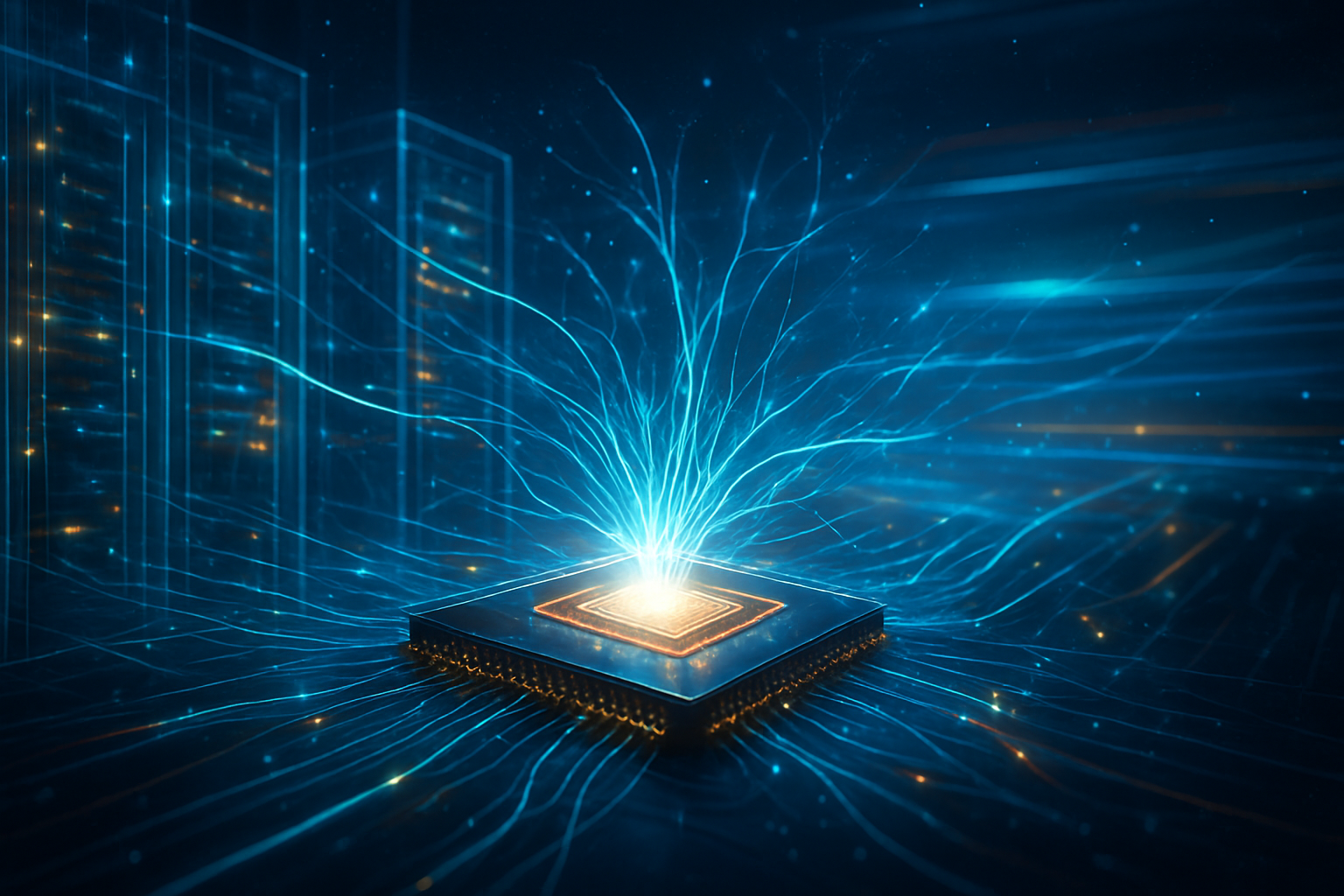
As of January 27, 2026, the artificial intelligence industry has officially hit the "Photonic Pivot." For years, the bottleneck of AI progress wasn't just the speed of the processor, but the speed at which data could move between them. Today, that bottleneck is being dismantled. Silicon Photonics, or Photonic Integrated Circuits (PICs), have moved from niche experimental tech to the foundational architecture of the world’s largest AI data centers. By replacing traditional copper-based electronic signals with pulses of light, the industry is finally breaking the "Copper Wall," enabling a new generation of gigascale AI factories that were physically impossible just 24 months ago.
The immediate significance of this shift cannot be overstated. As AI models scale toward trillions of parameters, the energy required to push electrons through copper wires has become a prohibitive tax on performance. Silicon Photonics reduces this energy cost by orders of magnitude while simultaneously doubling the bandwidth density. This development effectively realizes Item 14 on our annual Top 25 AI Trends list—the move toward "Photonic Interconnects"—marking a transition from the era of the electron to the era of the photon in high-performance computing (HPC).
The Technical Leap: From 1.6T Modules to Co-Packaged Optics
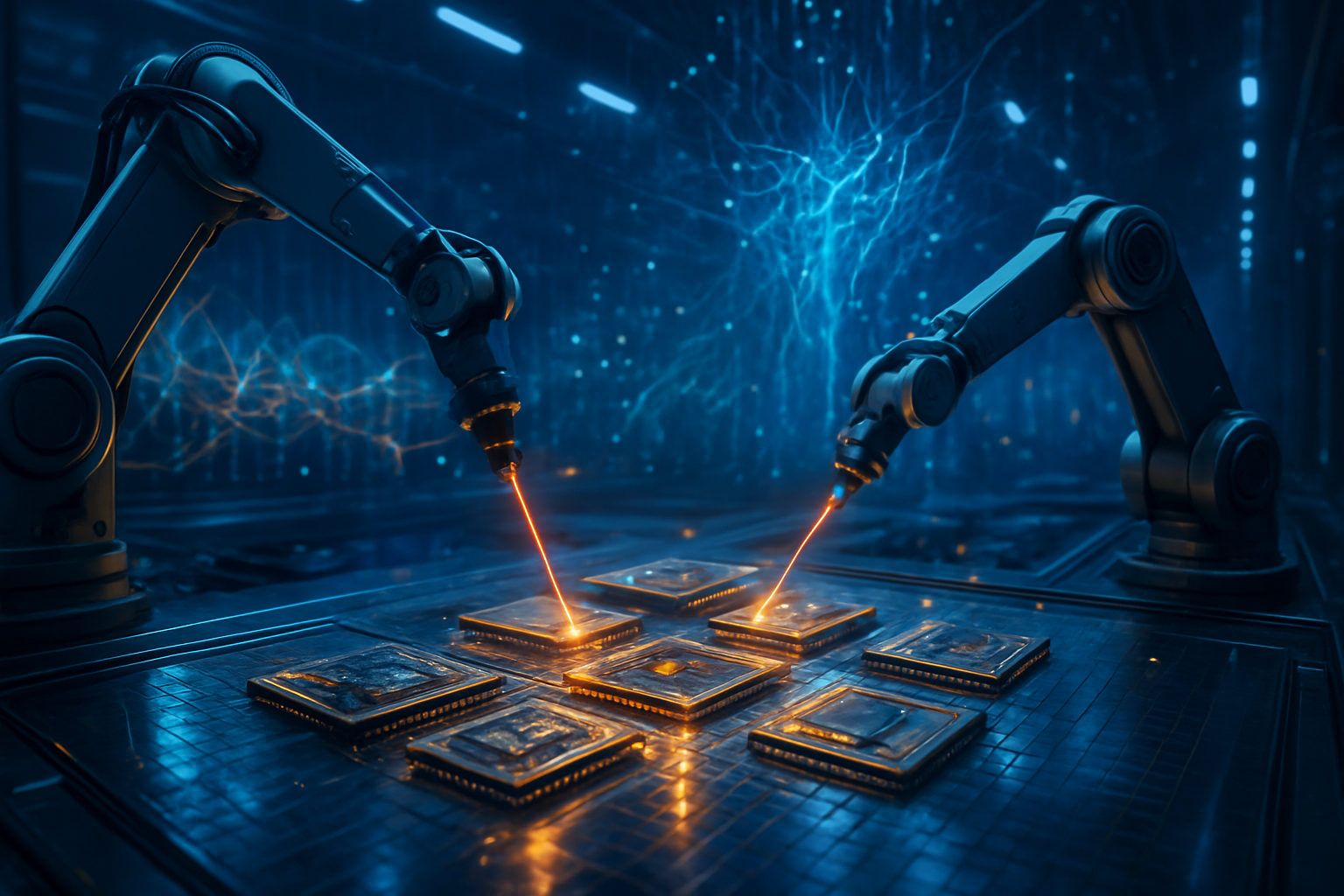
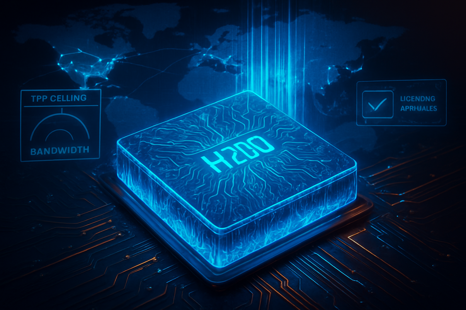
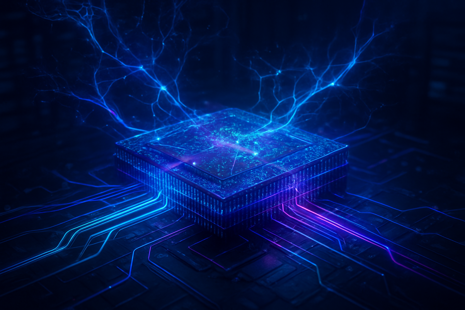
The technical breakthrough anchoring this revolution is the commercial maturation of 1.6 Terabit (1.6T) and early-stage 3.2T optical engines. Unlike traditional pluggable optics that sit at the edge of a server rack, the new standard is Co-Packaged Optics (CPO). In this architecture, companies like Broadcom (NASDAQ: AVGO) and NVIDIA (NASDAQ: NVDA) are integrating optical engines directly onto the GPU or switch package. This reduces the electrical path length from centimeters to millimeters, slashing power consumption from 20-30 picojoules per bit (pJ/bit) down to less than 5 pJ/bit. By minimizing "signal integrity" issues that plague copper at 224 Gbps per lane, light-based movement allows for data transmission over hundreds of meters with near-zero latency.
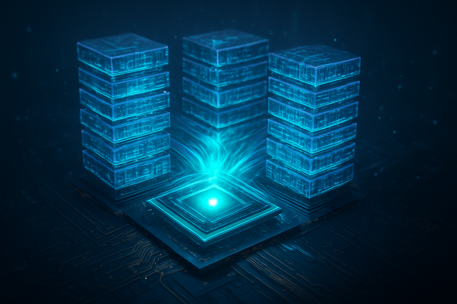
Furthermore, the introduction of the UALink (Ultra Accelerator Link) standard has provided a unified language for these light-based systems. This differs from previous approaches where proprietary interconnects created "walled gardens." Now, with the integration of Intel (NASDAQ: INTC)’s Optical Compute Interconnect (OCI) chiplets, data centers can disaggregate their resources. This means a GPU can access memory located three racks away as if it were on its own board, effectively solving the "Memory Wall" that has throttled AI performance for a decade. Industry experts note that this transition is equivalent to moving from a narrow gravel road to a multi-lane fiber-optic superhighway.
The Corporate Battlefield: Winners in the Luminous Era
The market implications of the photonic shift are reshaping the semiconductor landscape. NVIDIA (NASDAQ: NVDA) has maintained its lead by integrating advanced photonics into its newly released Rubin architecture. The Vera Rubin GPUs utilize these optical fabrics to link millions of cores into a single cohesive "Super-GPU." Meanwhile, Broadcom (NASDAQ: AVGO) has emerged as the king of the switch, with its Tomahawk 6 platform providing an unprecedented 102.4 Tbps of switching capacity, almost entirely driven by silicon photonics. This has allowed Broadcom to capture a massive share of the infrastructure spend from hyperscalers like Alphabet (NASDAQ: GOOGL) and Meta (NASDAQ: META).
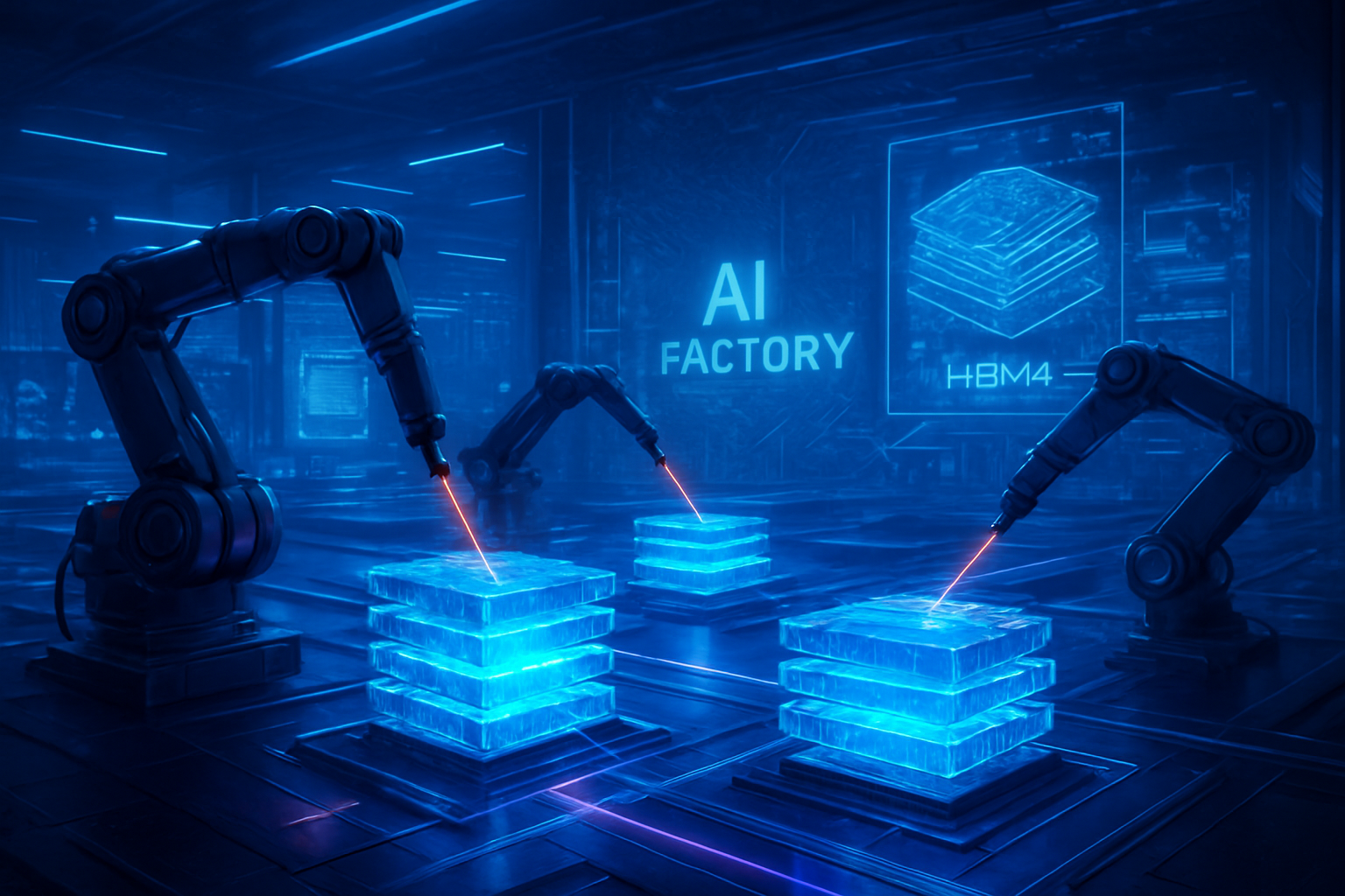
Marvell Technology (NASDAQ: MRVL) has also positioned itself as a primary beneficiary through its aggressive acquisition strategy, including the recent integration of Celestial AI’s photonic fabric technology. This move has allowed Marvell to dominate the "3D Silicon Photonics" market, where optical I/O is stacked vertically on chips to save precious "beachfront" space for more High Bandwidth Memory (HBM4). For startups and smaller AI labs, the availability of standardized optical components means they can now build high-performance clusters without the multi-billion dollar R&D budget previously required to overcome electronic signaling hurdles, leveling the playing field for specialized AI applications.
Beyond Bandwidth: The Wider Significance of Light
The transition to Silicon Photonics is not just about speed; it is a critical response to the global AI energy crisis. As of early 2026, data centers consume a staggering percentage of global electricity. By shifting to light-based data movement, the power overhead of data transmission—which previously accounted for up to 40% of a data center's energy profile—is being cut in half. This aligns with global sustainability goals and prevents a hard ceiling on AI growth. It fits into the broader trend of "Environmental AI," where efficiency is prioritized alongside raw compute power.
Comparing this to previous milestones, the "Photonic Pivot" is being viewed as more significant than the transition from HDD to SSD. While SSDs sped up data access, Silicon Photonics is changing the very topology of computing. We are moving away from discrete "boxes" of servers toward a "liquid" infrastructure where compute, memory, and storage are a fluid pool of resources connected by light. However, this shift does raise concerns regarding the complexity of manufacturing. The precision required to align microscopic lasers and fiber-optic strands on a silicon die remains a significant hurdle, leading to a supply chain that is currently more fragile than the traditional electronic one.
The Road Ahead: Optical Computing and Disaggregation
Looking toward 2027 and 2028, the next frontier is "Optical Computing"—where light doesn't just move the data but actually performs the mathematical calculations. While we are currently in the "interconnect phase," labs at Intel (NASDAQ: INTC) and various well-funded startups are already prototyping photonic tensor cores that could perform AI inference at the speed of light with almost zero heat generation. In the near term, expect to see the total "disaggregation" of the data center, where the physical constraints of a "server" disappear entirely, replaced by rack-scale or even building-scale "virtual" processors.
The challenges remaining are largely centered on yield and thermal management. Integrating lasers onto silicon—a material that historically does not emit light well—requires exotic materials and complex "hybrid bonding" techniques. Experts predict that as manufacturing processes mature, the cost of these optical integrated circuits will plummet, eventually bringing photonic technology out of the data center and into high-end consumer devices, such as AR/VR headsets and localized AI workstations, by the end of the decade.
Conclusion: The Era of the Photon has Arrived
The emergence of Silicon Photonics as the standard for AI infrastructure marks a definitive chapter in the history of technology. By breaking the electronic bandwidth limits that have constrained Moore's Law, the industry has unlocked a path toward artificial general intelligence (AGI) that is no longer throttled by copper and heat. The "Photonic Pivot" of 2026 will be remembered as the moment the physical architecture of the internet caught up to the ethereal ambitions of AI software.
For investors and tech leaders, the message is clear: the future is luminous. As we move through the first quarter of 2026, keep a close watch on the yield rates of CPO manufacturing and the adoption of the UALink standard. The companies that master the integration of light and silicon will be the architects of the next century of computing. The "Copper Wall" has fallen, and in its place, a faster, cooler, and more efficient future is being built—one photon at a time.
This content is intended for informational purposes only and represents analysis of current AI developments.
TokenRing AI delivers enterprise-grade solutions for multi-agent AI workflow orchestration, AI-powered development tools, and seamless remote collaboration platforms.
For more information, visit https://www.tokenring.ai/.