As the tech industry pivots into 2026, NVIDIA (NASDAQ: NVDA) has fundamentally shifted the theater of war in the artificial intelligence sector. No longer is the battle fought solely on transistor counts or software moats; the new frontier is "advanced packaging." By securing approximately 60% of Taiwan Semiconductor Manufacturing Company's (NYSE: TSM) total Chip-on-Wafer-on-Substrate (CoWoS) capacity for the fiscal year—estimated at a staggering 700,000 to 850,000 wafers—NVIDIA has effectively cornered the market on the high-performance hardware necessary to power the next generation of autonomous AI agents.
The announcement of the 'Rubin' platform (R100) at CES 2026 marks the official transition from the Blackwell architecture to a system-on-rack paradigm designed specifically for "Agentic AI." With this strategic lock on TSMC’s production lines, industry analysts have dubbed advanced packaging the "new currency" of the tech sector. While competitors scramble for the remaining 40% of the world's high-end assembly capacity, NVIDIA has built a logistical moat that may prove even more formidable than its CUDA software dominance.
The Technical Leap: R100, HBM4, and the Vera Architecture
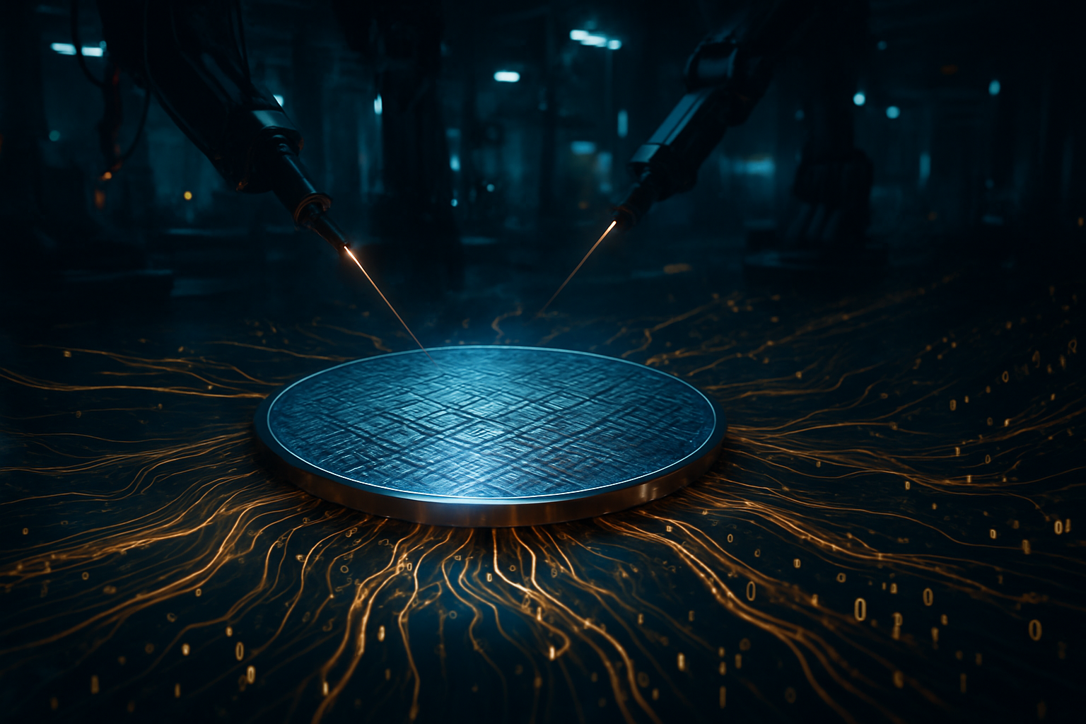
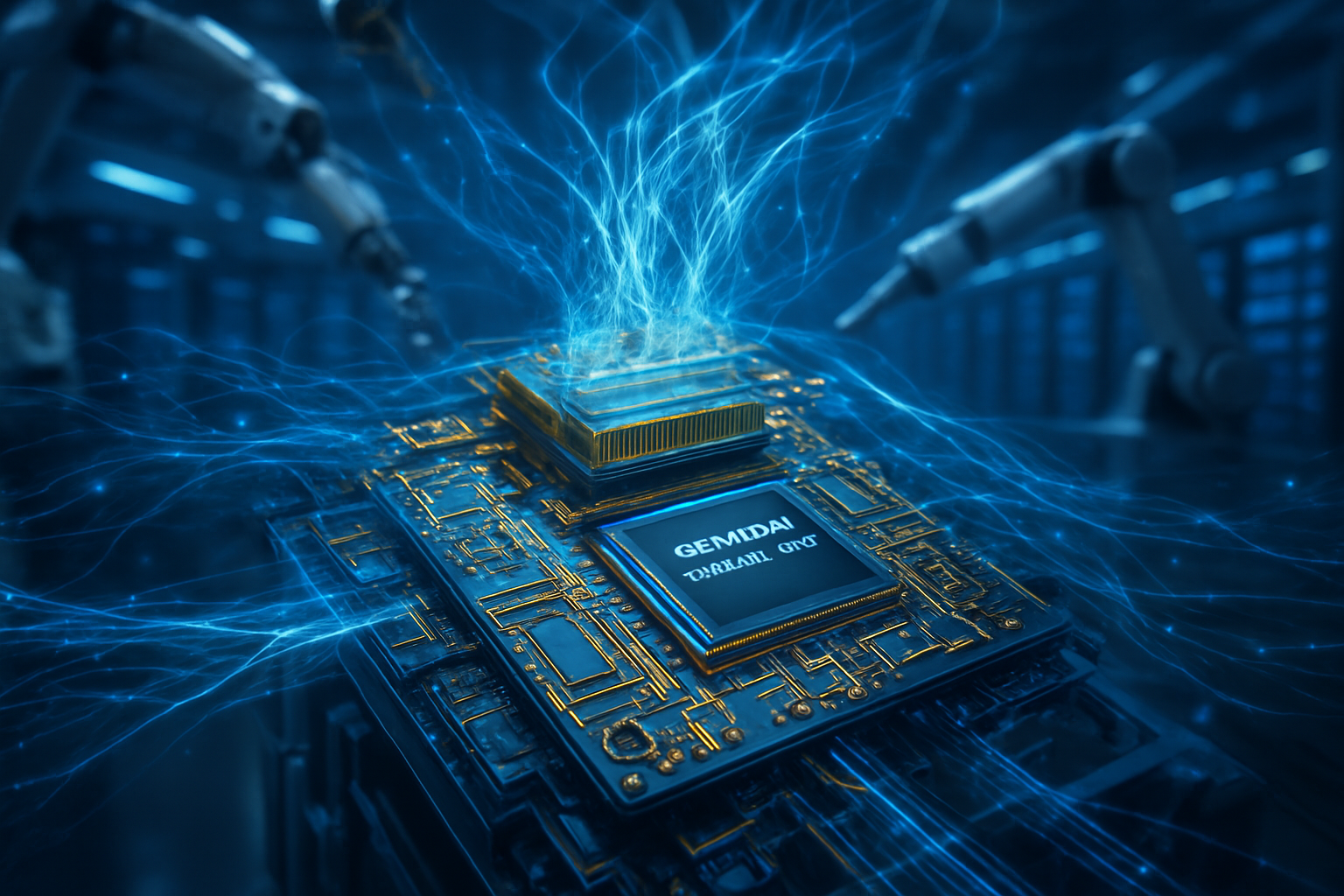
The Rubin R100 is more than an incremental upgrade; it is a specialized engine for the era of reasoning. Manufactured on TSMC’s enhanced 3nm (N3P) process, the Rubin GPU packs a massive 336 billion transistors—a 1.6x density improvement over the Blackwell series. However, the most critical technical shift lies in the memory. Rubin is the first platform to fully integrate HBM4 (High Bandwidth Memory 4), featuring eight stacks that provide 288GB of capacity and a blistering 22 TB/s of bandwidth. This leap is made possible by a 2048-bit interface, doubling the width of HBM3e and finally addressing the "memory wall" that has plagued large language model (LLM) scaling.
The platform also introduces the Vera CPU, which replaces the Grace series with 88 custom "Olympus" ARM cores. This CPU is architected to handle the complex orchestration required for multi-step AI reasoning rather than just simple data processing. To tie these components together, NVIDIA has transitioned entirely to CoWoS-L (Local Silicon Interconnect) packaging. This technology uses microscopic silicon bridges to "stitch" together multiple compute dies and memory stacks, allowing for a package size that is four to six times the limit of a standard lithographic reticle. Initial reactions from the research community highlight that Rubin’s 100-petaflop FP4 performance effectively halves the cost of token inference, bringing the dream of "penny-per-million-tokens" into reality.
A Supply Chain Stranglehold: Packaging as the Strategic Moat
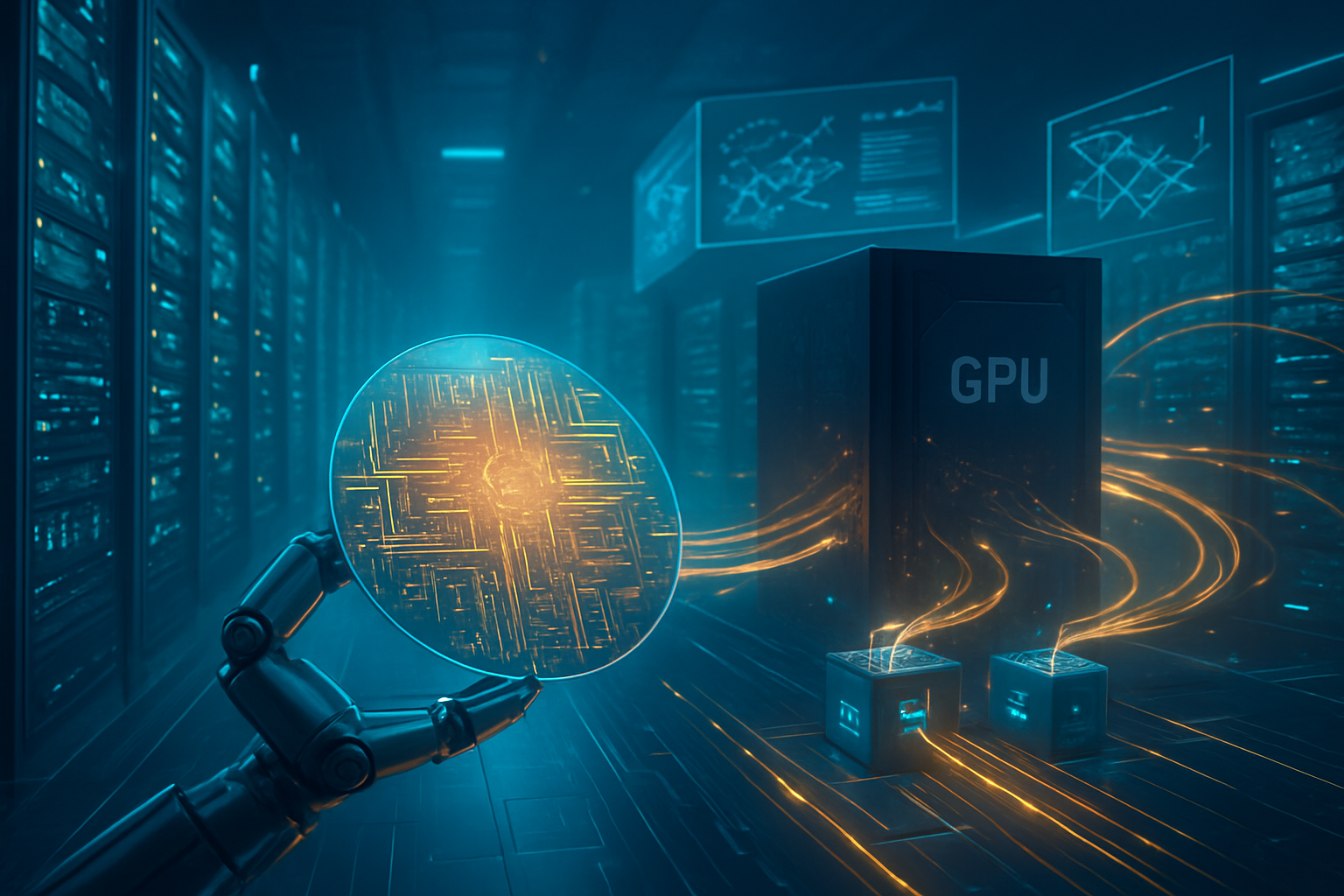
NVIDIA’s decision to book 60% of TSMC’s CoWoS capacity for 2026 has sent shockwaves through the competitive landscape. Advanced Micro Devices (NASDAQ: AMD) and Intel Corporation (NASDAQ: INTC) now find themselves in a high-stakes game of musical chairs. While AMD’s new Instinct MI400 offers a competitive 432GB of HBM4, its ability to scale to the demands of hyperscalers is now physically limited by the available slots at TSMC’s AP8 and AP7 fabs. Analysts at Wedbush have noted that in 2026, "having the best chip design is useless if you don't have the CoWoS allocation to build it."
In response to this bottleneck, major hyperscalers like Meta Platforms (NASDAQ: META) and Amazon (NASDAQ: AMZN) have begun diversifying their custom ASIC strategies. Meta has reportedly diverted a portion of its MTIA (Meta Training and Inference Accelerator) production to Intel’s packaging facilities in Arizona, utilizing Intel’s EMIB (Embedded Multi-Die Interconnect Bridge) technology as a hedge against the TSMC shortage. Despite these efforts, NVIDIA’s pre-emptive strike on the supply chain ensures that it remains the "default choice" for any organization looking to deploy AI at scale in the coming 24 months.
Beyond Generative AI: The Rise of Agentic Infrastructure
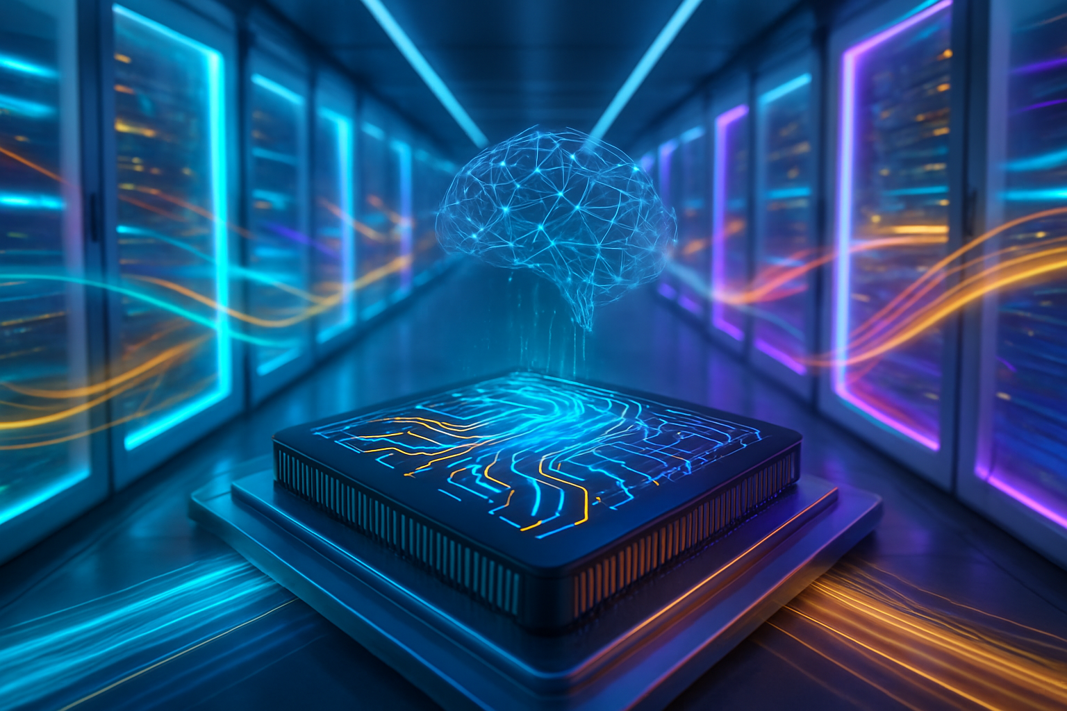
The broader significance of the Rubin platform lies in its optimization for "Agentic AI"—systems capable of autonomous planning and execution. Unlike the generative models of 2024 and 2025, which primarily predicted the next word in a sequence, 2026’s models are focused on "multi-turn reasoning." This shift requires hardware with ultra-low latency and persistent memory storage. NVIDIA has met this need by integrating Co-Packaged Optics (CPO) directly into the Rubin package, replacing copper transceivers with fiber optics to reduce inter-GPU communication power by 5x.
This development signals a maturation of the AI landscape from a "gold rush" of model training to a "utility phase" of execution. The Rubin NVL72 rack-scale system, which integrates 72 Rubin GPUs, acts as a single massive computer with 260 TB/s of aggregate bandwidth. This infrastructure is designed to support thousands of autonomous agents working in parallel on tasks ranging from drug discovery to automated software engineering. The concern among some industry watchdogs, however, is the centralization of this power. With NVIDIA controlling the packaging capacity, the pace of AI innovation is increasingly dictated by a single company’s roadmap.
The Future Roadmap: Glass Substrates and Panel-Level Scaling
Looking beyond the 2026 rollout of Rubin, NVIDIA and TSMC are already preparing for the next physical frontier: Fan-Out Panel-Level Packaging (FOPLP). Current CoWoS technology is limited by the circular 300mm silicon wafers on which chips are built, leading to significant wasted space at the edges. By 2027 and 2028, NVIDIA is expected to transition to large rectangular glass or organic panels (600mm x 600mm) for its "Feynman" architecture.
This transition will allow for three times as many chips per carrier, potentially easing the capacity constraints that defined the 2025-2026 era. Experts predict that glass substrates will become the standard by 2028, offering superior thermal stability and even higher interconnect density. However, the immediate challenge remains the yield rates of these massive panels. For now, the industry’s eyes are on the Rubin ramp-up in the second half of 2026, which will serve as the ultimate test of whether NVIDIA’s "packaging first" strategy can sustain its 1000% growth trajectory.
A New Chapter in Computing History
The launch of the Rubin platform and the strategic capture of TSMC’s CoWoS capacity represent a pivotal moment in semiconductor history. NVIDIA has successfully transformed itself from a chip designer into a vertically integrated infrastructure provider that controls the most critical bottlenecks in the global economy. By securing 60% of the world's most advanced assembly capacity, the company has effectively decided the winners and losers of the 2026 AI cycle before the first Rubin chip has even shipped.
In the coming months, the industry will be watching for the first production yields of the R100 and the success of HBM4 integration from suppliers like SK Hynix (KRX: 000660), Samsung Electronics (KRX: 005930), and Micron Technology (NASDAQ: MU). As packaging continues to be the "new currency," the ability to innovate within these physical constraints will define the next decade of artificial intelligence. For now, the "Rubin Era" has begun, and the world’s compute capacity is firmly in NVIDIA’s hands.
This content is intended for informational purposes only and represents analysis of current AI developments.
TokenRing AI delivers enterprise-grade solutions for multi-agent AI workflow orchestration, AI-powered development tools, and seamless remote collaboration platforms.
For more information, visit https://www.tokenring.ai/.