Tag: Nvidia

  • NVIDIA H200s Cleared for China: Inside the Trump Administration’s Bold High-Stakes Tech Thaw

    NVIDIA H200s Cleared for China: Inside the Trump Administration’s Bold High-Stakes Tech Thaw

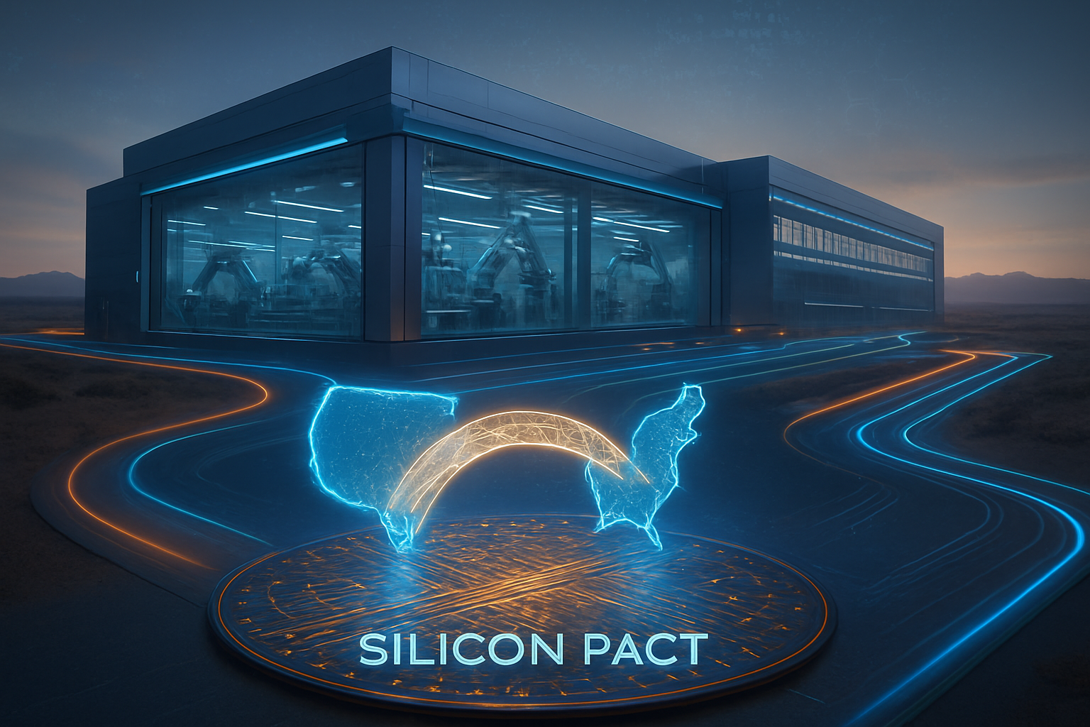
    In a move that has sent shockwaves through both Silicon Valley and Beijing, the Trump administration has officially authorized the export of NVIDIA H200 GPU accelerators to the Chinese market. The decision, finalized in late January 2026, marks a dramatic reversal of the multi-year "presumption of denial" policy that had effectively crippled the sales of high-end American AI hardware to China. By replacing blanket bans with a transactional, security-monitored framework, the U.S. government aims to reassert American influence over global AI ecosystems while capturing significant federal revenue from the world’s second-largest economy.

    The policy shift is being hailed by industry leaders as a pragmatic "thaw" in tech relations, though it comes with a complex web of restrictions that distinguish it from the unrestricted trade of the past decade. For NVIDIA (NASDAQ: NVDA), the announcement represents a lifeline for its Chinese business, which had previously been relegated to selling "degraded" or lower-performance chips like the H20 to comply with strict 2023 and 2024 export controls. Under the new regime, the H200—one of the most powerful AI training and inference chips currently in production—will finally be available to vetted Chinese commercial entities.

    Advanced Silicon and the "Vulnerability Screening" Mandate

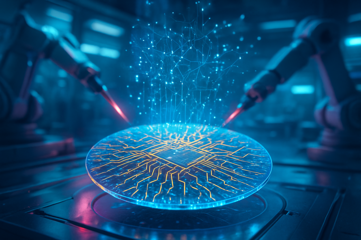
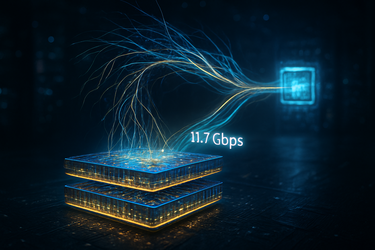
    The technical specifications of the NVIDIA H200 represent a massive leap forward for the Chinese AI industry. Built on the Hopper architecture, the H200 is the first GPU to feature HBM3e memory, delivering 141GB of capacity and 4.8 TB/s of memory bandwidth. Compared to the H100, the H200 offers nearly double the inference performance for large language models (LLMs) like Llama 3 or GPT-4. This bandwidth is the critical factor in modern AI scaling, and its availability in China is expected to dramatically shorten the training cycles for domestic Chinese models which had been stagnating under previous hardware constraints.

    To maintain a strategic edge, the U.S. Department of Commerce’s Bureau of Industry and Security (BIS) has introduced a new "regulatory sandwich." Under the January 13, 2026 ruling, chips are permitted for export only if their Total Processing Performance (TPP) remains below 21,000 and DRAM bandwidth stays under 6,500 GB/s. While the H200 fits within these specific bounds, the administration has eliminated the practice of "binning" or hardware-level performance capping for the Chinese market. Instead, the focus has shifted to who is using the chips and how they are being deployed.

    A key technical innovation in this policy is the "U.S. First" testing protocol. Before any H200 units are shipped to China, they must first be imported from manufacturing hubs into specialized American laboratories. There, they undergo "vulnerability screening" and technical verification to ensure no unauthorized firmware modifications have been made. This allows the U.S. government to maintain a literal hands-on check on the hardware before it enters the Chinese supply chain, a logistical hurdle that experts say is unprecedented in the history of semiconductor trade.

    Initial reactions from the AI research community have been cautiously optimistic. While researchers at institutions like Tsinghua University welcome the performance boost, there is lingering skepticism regarding the mandatory U.S. testing phase. Industry analysts note that this requirement could introduce a 4-to-6 week delay in the supply chain. However, compared to the alternative—developing sovereign silicon that still lags generations behind NVIDIA—most Chinese tech giants see this as a necessary price for performance.

    Revenue Levies and the Battle for Market Dominance

    The financial implications for NVIDIA are profound. Before the 2023 restrictions, China accounted for approximately 20% to 25% of NVIDIA’s data center revenue. This figure had plummeted as Chinese firms were forced to choose between underpowered U.S. chips and domestic alternatives. With the H200 now on the table, analysts predict a massive surge in capital expenditure from Chinese "hyperscalers" such as Alibaba (NYSE: BABA), Tencent (HKG: 0700), and Baidu (NASDAQ: BIDU). These companies have been eager to upgrade their aging infrastructure to compete with Western AI capabilities.

    However, the "Trump Thaw" is far from a free pass. The administration has imposed a mandatory 25% "revenue levy" on all H200 sales to China, structured as a Section 232 national security tariff. This ensures that the U.S. Treasury benefits directly from every transaction. Additionally, NVIDIA is subject to volume caps: the total number of H200s exported to China cannot exceed 50% of the volume sold to U.S. domestic customers. This "America First" ratio is designed to ensure that the U.S. always maintains a larger, more advanced install base of AI compute power.

    The move also places intense pressure on Advanced Micro Devices (NASDAQ: AMD), which has been seeking its own licenses for the Instinct MI325X series. As the market opens, a new competitive landscape is emerging where U.S. companies are not just competing against each other, but against the rising tide of Chinese domestic competitors like Huawei. By allowing the H200 into China, the U.S. is effectively attempting to "crowd out" Huawei’s Ascend 910C chips, making it harder for Chinese firms to justify the switch to a domestic ecosystem that remains more difficult to program for.

    Strategic advantages for ByteDance—the parent company of TikTok—are also in the spotlight. ByteDance has historically been one of NVIDIA's largest customers in Asia, using GPUs for its massive recommendation engines and generative AI projects. The ability to legally procure H200s gives ByteDance a clear path to maintaining its global competitive edge, provided it can navigate the stringent end-user vetting processes required by the new BIS rules.

    The Geopolitical "AI Overwatch" and a Fragile Thaw

    The broader significance of this decision cannot be overstated. It signals a shift in the U.S. strategy from total containment to a "managed dependency." By allowing China to buy NVIDIA’s second-best hardware (with the newer Blackwell architecture still largely restricted), the U.S. keeps the Chinese tech sector tethered to American software stacks like CUDA. Experts argue that if China were forced to fully decouple, they would eventually succeed in building a parallel, independent tech ecosystem. This policy is an attempt to delay that "Sputnik moment" indefinitely.

    This strategy has not been without fierce domestic opposition. On January 21, 2026, the House Foreign Affairs Committee advanced the "AI Overwatch Act" (H.R. 6875), a bipartisan effort to grant Congress the power to veto specific export licenses. Critics of the administration, including many "China hawks," argue that the H200 is too powerful to be exported safely. They contend that the 25% tariff is a "pay-to-play" scheme that prioritizes corporate profits and short-term federal revenue over long-term national security, fearing that the hardware will inevitably be diverted to military AI projects.

    Comparing this to previous AI milestones, such as the 2022 ban on the A100, the current situation represents a much more transactional approach to geopolitics. The administration's "AI and Crypto Czar," David Sacks, has defended the policy by stating that the U.S. must lead the global AI ecosystem through engagement rather than isolation. The "thaw" is seen as a way to lower the temperature on trade relations while simultaneously building a massive federal war chest funded by Chinese tech spending.

    Beijing’s response has been characteristically measured but complex. While the Ministry of Industry and Information Technology (MIIT) has granted "in-principle" approval for firms to order H200s, they have also reportedly mandated that for every U.S. chip purchased, a corresponding investment must be made in domestic silicon. This "one-for-one" quota system indicates that while China is happy to have access to NVIDIA’s power, it remains fully committed to its long-term goal of self-reliance.

    Future Developments: Blackwell and the Parity Race

    As we look toward the remainder of 2026, the primary question is whether this policy will extend to NVIDIA’s next-generation Blackwell architecture. Currently, the B200 remains restricted, keeping the "performance gap" between the U.S. and China at approximately 12 to 18 months. However, if the H200 export experiment is deemed a financial and security success, there is already talk in Washington of a "Blackwell Lite" variant being introduced by 2027.

    The near-term focus will be on the logistical execution of the "vulnerability screening" labs. If these facilities become a bottleneck, it could lead to renewed friction between the White House and the tech industry. Furthermore, the world will be watching to see if other nations, particularly in the Middle East and Southeast Asia, demand similar "case-by-case" license review policies to access the highest tiers of American compute power.

    Predicting the next moves of the Chinese "national champions" is also vital. With access to H200s, will Alibaba and Baidu finally reach parity with U.S.-based models like Claude or Gemini? Or will the U.S. domestic volume caps ensure that American labs always have a two-to-one advantage in raw compute? Most experts believe that while the H200 will prevent a total collapse of the Chinese AI sector, the structural advantages of the U.S. ecosystem—combined with the new 25% "AI Tax"—will keep the American lead intact.

    A New Chapter in the Silicon Cold War

    The approval of NVIDIA H200 exports to China is a defining moment in the history of artificial intelligence and international trade. It represents a pivot from the "small yard, high fence" strategy toward a more dynamic "toll-booth" model. By allowing high-performance hardware to flow into China under strict supervision and high taxation, the Trump administration is betting that economic interdependency can be used as a tool for national security rather than a vulnerability.

    In the coming weeks, the industry will watch closely for the first confirmed shipments of H200s landing in Shanghai and the resulting benchmarks from Chinese AI labs. The success or failure of this policy will likely dictate the trajectory of U.S.-China relations for the rest of the decade. If the H200s are used to create breakthroughs that threaten U.S. interests, the "AI Overwatch Act" will almost certainly be invoked to shut the gates once again.

    Ultimately, the H200 export decision is a high-stakes gamble. It provides NVIDIA and the U.S. Treasury with a massive financial windfall while offering China the tools it needs to stay in the AI race. Whether this leads to a stable "technological co-existence" or merely fuels the next phase of an escalating AI arms race remains the most critical question of 2026.


    This content is intended for informational purposes only and represents analysis of current AI developments.

    TokenRing AI delivers enterprise-grade solutions for multi-agent AI workflow orchestration, AI-powered development tools, and seamless remote collaboration platforms.
    For more information, visit https://www.tokenring.ai/.

  • The Memory Wall: Why HBM4 Is Now the Most Scarce Commodity on Earth

    The Memory Wall: Why HBM4 Is Now the Most Scarce Commodity on Earth

    As of January 2026, the artificial intelligence revolution has hit a physical limit not defined by code or algorithms, but by the physical availability of High Bandwidth Memory (HBM). What was once a niche segment of the semiconductor market has transformed into the "currency of AI," with industry leaders SK Hynix (KRX: 000660) and Micron (NASDAQ: MU) officially announcing that their production lines are entirely sold out through the end of 2026. This unprecedented scarcity has triggered a global scramble among tech giants, turning the silicon supply chain into a high-stakes geopolitical battlefield where the ability to secure memory determines which companies will lead the next era of generative intelligence.

    The immediate significance of this shortage cannot be overstated. As NVIDIA (NASDAQ: NVDA) transitions from its Blackwell architecture to the highly anticipated Rubin platform, the demand for next-generation HBM4 has decoupled from traditional market cycles. We are no longer witnessing a standard supply-and-demand fluctuation; instead, we are seeing the emergence of a structural "memory tax" on all high-end computing. With lead times for new orders effectively non-existent, the industry is bracing for a two-year period where the growth of AI model parameters may be capped not by innovation, but by the sheer volume of memory stacks available to feed the GPUs.

    The Technical Leap to HBM4

    The transition from HBM3e to HBM4 represents the most significant architectural overhaul in the history of memory technology. While HBM3e served as the workhorse for the 2024–2025 AI boom, HBM4 is a fundamental redesign aimed at shattering the "Memory Wall"—the bottleneck where processor speed outpaces the rate at which data can be retrieved. The most striking technical leap in HBM4 is the doubling of the interface width from 1,024 bits per stack to a massive 2,048-bit bus. This allows for bandwidth speeds exceeding 2.0 TB/s per stack, a necessity for the massive "Mixture of Experts" (MoE) models that now dominate the enterprise AI landscape.

    Unlike previous generations, HBM4 moves away from a pure memory manufacturing process for its "base die"—the foundation layer that communicates with the GPU. For the first time, memory manufacturers are collaborating with foundries like TSMC (NYSE: TSM) to build these base dies using advanced logic processes, such as 5nm or 12nm nodes. This integration allows for customized logic to be embedded directly into the memory stack, significantly reducing latency and power consumption. By offloading certain data-shuffling tasks to the memory itself, HBM4 enables AI accelerators to spend more cycles on actual computation rather than waiting for data packets to arrive.

    The initial reactions from the AI research community have been a mix of awe and anxiety. Experts at major labs note that while HBM4’s 12-layer and 16-layer configurations provide the necessary "vessel" for trillion-parameter models, the complexity of manufacturing these stacks is staggering. The industry is moving toward "hybrid bonding" techniques, which replace traditional microbumps with direct copper-to-copper connections. This is a delicate, low-yield process that explains why supply remains so constrained despite massive capital expenditures by the world’s big three memory makers.

    Market Winners and Strategic Positioning

    This scarcity creates a distinct "haves and have-nots" divide among technology giants. NVIDIA (NASDAQ: NVDA) remains the primary beneficiary of its early and aggressive securing of HBM capacity, effectively "cornering the market" for its upcoming Rubin GPUs. However, even the king of AI chips is feeling the squeeze, as it must balance its allocations between long-standing partners and the surging demand from sovereign AI projects. Meanwhile, competitors like Advanced Micro Devices (NASDAQ: AMD) and specialized AI chip startups find themselves in a precarious position, often forced to settle for previous-generation HBM3e or wait in a years-long queue for HBM4 allocations.

    For tech giants like Google (NASDAQ: GOOGL) and Amazon (NASDAQ: AMZN), the shortage has accelerated the development of custom in-house silicon. By designing their own TPU and Trainium chips to work with specific memory configurations, these companies are attempting to bypass the generic market shortage. However, they remain tethered to the same handful of memory suppliers. The strategic advantage has shifted from who has the best algorithm to who has the most secure supply agreement with SK Hynix or Micron. This has led to a surge in "pre-payment" deals, where cloud providers are fronting billions of dollars in capital just to reserve production capacity for 2027 and beyond.

    Samsung Electronics (KRX: 005930) is currently the "wild card" in this corporate chess match. After trailing SK Hynix in HBM3e yields for much of 2024 and 2025, Samsung has reportedly qualified its 12-stack HBM3e for major customers and is aggressively pivoting to HBM4. If Samsung can achieve stable yields on its HBM4 production line in 2026, it could potentially alleviate some market pressure. However, with SK Hynix and Micron already booked solid, Samsung’s capacity is being viewed as the last available "lifeboat" for companies that failed to secure early contracts.

    The Global Implications of the $13 Billion Bet

    The broader significance of the HBM shortage lies in the physical realization that AI is not an ethereal cloud service, but a resource-intensive industrial product. The $13 billion investment by SK Hynix in its new "P&T7" advanced packaging facility in Cheongju, South Korea, signals a paradigm shift in the semiconductor industry. Packaging—the process of stacking and connecting chips—has traditionally been a lower-margin "back-end" activity. Today, it is the primary bottleneck. This $13 billion facility is essentially a fortress dedicated to the microscopic precision required to stack 16 layers of DRAM with near-zero failure rates.

    This shift toward "advanced packaging" as the center of gravity for AI hardware has significant geopolitical and economic implications. We are seeing a massive concentration of critical infrastructure in a few specific geographic nodes, making the AI supply chain more fragile than ever. Furthermore, the "HBM tax" is spilling over into the consumer market. Because HBM production consumes three times the wafer capacity of standard DDR5 DRAM, manufacturers are reallocating their resources. This has caused a 60% surge in the price of standard RAM for PCs and servers over the last year, as the world's memory fabs prioritize the high-margin "currency of AI."

    Comparatively, this milestone echoes the early days of the oil industry or the lithium rush for electric vehicles. HBM4 has become the essential fuel for the modern economy. Without it, the "Large Language Models" and "Agentic Workflows" that businesses now rely on would grind to a halt. The potential concern is that this "memory wall" could slow the pace of AI democratization, as only the wealthiest corporations and nations can afford to pay the premium required to jump the queue for these critical components.

    Future Horizons: Beyond HBM4

    Looking ahead, the road to 2027 will be defined by the transition to HBM4E (the "extended" version of HBM4) and the maturation of 3D integration. Experts predict that by 2027, the industry will move toward "Logic-DRAM 3D Integration," where the GPU and the HBM are not just side-by-side on a substrate but are stacked directly on top of one another. This would virtually eliminate data travel distance, but it presents monumental thermal challenges that have yet to be fully solved. If 2026 is the year of HBM4, 2027 will be the year the industry decides if it can handle the heat.

    Near-term developments will focus on improving yields. Current estimates suggest that HBM4 yields are significantly lower than those of standard memory, often hovering between 40% and 60%. As SK Hynix and Micron refine their processes, we may see a slight easing of supply toward the end of 2026, though most analysts expect the "sold-out" status to persist as new AI applications—such as real-time video generation and autonomous robotics—require even larger memory pools. The challenge will be scaling production fast enough to meet the voracious appetite of the "AI Beast" without compromising the reliability of the chips.

    Summary and Outlook

    In summary, the HBM4 shortage of 2026 is the defining hardware story of the mid-2020s. The fact that the world’s leading memory producers are sold out through 2026 underscores the sheer scale of the AI infrastructure build-out. SK Hynix and Micron have successfully transitioned from being component suppliers to becoming the gatekeepers of the AI era, while the $13 billion investment in packaging facilities marks the beginning of a new chapter in semiconductor manufacturing where "stacking" is just as important as "shrinking."

    As we move through the coming months, the industry will be watching Samsung’s yield rates and the first performance benchmarks of NVIDIA’s Rubin architecture. The significance of HBM4 in AI history will be recorded as the moment when the industry moved past pure compute power and began to solve the data movement problem at a massive, industrial scale. For now, the "currency of AI" remains the rarest and most valuable asset in the tech world, and the race to secure it shows no signs of slowing down.


    This content is intended for informational purposes only and represents analysis of current AI developments.

    TokenRing AI delivers enterprise-grade solutions for multi-agent AI workflow orchestration, AI-powered development tools, and seamless remote collaboration platforms.
    For more information, visit https://www.tokenring.ai/.

  • The Silicon Pact: US and Taiwan Ink Historic 2026 Trade Deal to Reshore AI Chip Supremacy

    The Silicon Pact: US and Taiwan Ink Historic 2026 Trade Deal to Reshore AI Chip Supremacy

    In a move that fundamentally redraws the map of the global technology sector, the United States and Taiwan officially signed the “Agreement on Trade & Investment” on January 15, 2026. Dubbed the “Silicon Pact” by industry leaders, this landmark treaty represents the most significant restructuring of the semiconductor supply chain in decades. The agreement aims to secure the hardware foundations of the artificial intelligence era by aggressively reshoring manufacturing capabilities to American soil, ensuring that the next generation of AI breakthroughs is powered by domestically produced silicon.

    The signing of the deal marks a strategic victory for the U.S. goal of establishing “sovereign AI infrastructure.” By offering unprecedented duty exemptions and facilitating a massive influx of capital, the agreement seeks to mitigate the risks of geopolitical instability in the Taiwan Strait. For Taiwan, the pact strengthens its “Silicon Shield” by deepening economic and security ties with its most critical ally, even as it navigates the complex logistics of migrating its most valuable industrial assets across the Pacific.

    A Technical Blueprint for Reshoring: Duty Exemptions and the 2.5x Rule

    At the heart of the Silicon Pact are highly specific trade mechanisms designed to overcome the prohibitive costs of building high-end semiconductor fabrication plants (fabs) in the United States. A standout provision is the historic "Section 232" duty exemption. Under these terms, Taiwanese companies investing in U.S. capacity are granted "most favored nation" status, allowing them to import up to 2.5 times their planned U.S. production capacity in semiconductors and wafers duty-free during the construction phase of their American facilities. Once these fabs are operational, the exemption continues, permitting the import of 1.5 times their domestic production capacity without the burden of Section 232 duties.

    This technical framework is supported by a massive financial commitment. Taiwanese firms have pledged at least $250 billion in new direct investments into U.S. semiconductor, energy, and AI sectors. To facilitate this migration, the Taiwanese government is providing an additional $250 billion in credit guarantees to help small and medium-sized suppliers—the essential chemical, lithography, and testing firms—replicate their ecosystem within the United States. This "ecosystem-in-a-box" approach differs from previous subsidy-only models by focusing on the entire vertical supply chain rather than just the primary manufacturing sites.

    Initial reactions from the AI research community have been largely positive, though tempered by the reality of the engineering challenges ahead. Experts at the Taiwan Institute of Economic Research (TIER) note that while the deal provides the financial and legal "rails" for reshoring, the technical execution remains a gargantuan task. The goal is to shift the production of advanced AI chips from a nearly 100% Taiwan-centric model to an 85-15 split by 2030, eventually reaching an 80-20 split by 2036. This transition is seen as essential for the hardware demands of "GPT-6 class" models, which require specialized, high-bandwidth memory and advanced packaging that currently reside almost exclusively in Taiwan.

    Corporate Winners and the $250 Billion Reinvestment

    The primary beneficiary and anchor of this deal is Taiwan Semiconductor Manufacturing Co. (NYSE: TSM). Under the new agreement, TSMC is expected to expand its total U.S. investment to an estimated $165 billion, encompassing multiple advanced gigafabs in Arizona and potentially other states. This massive commitment is a direct response to the demands of its largest customers, including Apple Inc. (NASDAQ: AAPL) and Nvidia Corporation (NASDAQ: NVDA), both of which have been vocal about the need for a "geopolitically resilient" supply of the H-series and B-series chips that power their AI data centers.

    For U.S.-based chipmakers like Intel Corporation (NASDAQ: INTC) and Advanced Micro Devices, Inc. (NASDAQ: AMD), the Silicon Pact presents a double-edged sword. While it secures the domestic supply chain and may provide opportunities for partnership in advanced packaging, it also brings their most formidable competitor—TSMC—directly into their backyard with significant federal and trade advantages. However, the strategic advantage for Nvidia and other AI labs is clear: they can now design next-generation architectures with the assurance that their physical production is shielded from potential maritime blockades or regional conflicts.

    The deal also triggers a secondary wave of disruption for the broader tech ecosystem. With $250 billion in credit guarantees flowing to upstream suppliers, we are likely to see a "brain drain" of specialized engineering talent moving from Hsinchu to new industrial hubs in the American Southwest. This migration will likely disadvantage any companies that remain tethered to the older, more vulnerable supply chains, effectively creating a "premium" tier of AI hardware that is "Made in America" with Taiwanese expertise.

    Geopolitics and the "Democratic" Supply Chain

    The broader significance of the Silicon Pact cannot be overstated; it is a definitive step toward the bifurcation of the global tech economy. Taipei officials have framed the agreement as the foundation of a "democratic" supply chain, a direct ideological and economic counter to China’s influence in the Pacific. By decoupling the most advanced AI hardware production from the immediate vicinity of mainland China, the U.S. is effectively insulating its most critical technological asset—AI—from geopolitical leverage.

    Unsurprisingly, the deal has drawn "stern opposition" from Beijing. China’s Ministry of Foreign Affairs characterized the pact as a violation of existing diplomatic norms and an attempt to "hollow out" the global economy. This tension highlights the primary concern of many international observers: that the Silicon Pact might accelerate the very conflict it seeks to mitigate by signaling a permanent shift in the strategic importance of Taiwan. Comparisons are already being drawn to the Cold War-era industrial mobilizations, though the complexity of 2-nanometer chip production makes this a far more intricate endeavor than the steel or aerospace races of the past.

    Furthermore, the deal addresses the growing trend of "AI Nationalism." As nations realize that AI compute is as vital as oil or electricity, the drive to control the physical hardware becomes paramount. The Silicon Pact is the first major international treaty that treats semiconductor fabs not just as commercial entities, but as essential national security infrastructure. It sets a precedent that could see similar deals between the U.S. and other tech hubs like South Korea or Japan in the near future.

    Challenges and the Road to 2029

    Looking ahead, the success of the Silicon Pact will hinge on solving several domestic hurdles that have historically plagued U.S. manufacturing. Near-term developments will focus on the construction of "world-class industrial parks" that can house the hundreds of support companies moving under the credit guarantee program. The ambitious target of moving 40% of the supply chain by 2029 is viewed by some analysts as "physically impossible" due to the shortage of specialized semiconductor engineers and the massive water and power requirements of these new "gigafabs."

    In the long term, we can expect the emergence of new AI applications that leverage this domestic hardware security. "Sovereign AI" clouds, owned and operated within the U.S. using chips manufactured in Arizona, will likely become the standard for government and defense-related AI projects. However, the industry must first address the "talent gap." Experts predict that the U.S. will need to train or import tens of thousands of specialized technicians and researchers to man these new facilities, a challenge that may require further legislative action on high-skilled immigration.

    A New Era for the Global Silicon Landscape

    The January 2026 US-Taiwan Trade Deal is a watershed moment that marks the end of the era of globalization driven solely by cost-efficiency. In its place, a new era of "Resilience-First" manufacturing has begun. The deal provides the financial incentives and legal protections necessary to move the world's most complex industrial process across an ocean, representing a massive bet on the continued dominance of AI as the primary driver of economic growth.

    The key takeaways are clear: the U.S. is willing to pay a premium for hardware security, and Taiwan is willing to export its industrial crown jewels to ensure its own survival. While the "hollowing-out" of Taiwan's domestic industry remains a valid concern for some, the Silicon Pact ensures that the democratic world remains at the forefront of the AI revolution. In the coming weeks and months, the tech industry will be watching closely as the first wave of Taiwanese suppliers begins the process of breaking ground on American soil.


    This content is intended for informational purposes only and represents analysis of current AI developments.

    TokenRing AI delivers enterprise-grade solutions for multi-agent AI workflow orchestration, AI-powered development tools, and seamless remote collaboration platforms.
    For more information, visit https://www.tokenring.ai/.

  • The 2nm Revolution: TSMC Ramps Volume Production of N2 Silicon to Fuel the AI Decade

    The 2nm Revolution: TSMC Ramps Volume Production of N2 Silicon to Fuel the AI Decade

    As of January 26, 2026, the semiconductor industry has officially entered a new epoch known as the "Angstrom Era." Taiwan Semiconductor Manufacturing Company (TSM: NYSE) has confirmed that its next-generation 2-nanometer (N2) process technology has successfully moved into high-volume manufacturing, marking a critical milestone for the global technology landscape. With mass production ramping up at the newly completed Hsinchu and Kaohsiung gigafabs, the industry is witnessing the most significant architectural shift in over a decade.

    This transition is not merely a routine shrink in transistor size; it represents a fundamental re-engineering of the silicon that powers everything from the smartphones in our pockets to the massive data centers training the next generation of artificial intelligence. With demand for AI compute reaching a fever pitch, TSMC’s N2 node is expected to be the exclusive engine for the world’s most advanced hardware, though industry analysts warn that a massive supply-demand imbalance will likely trigger shortages lasting well into 2027.

    The Architecture of the Future: Transitioning to GAA Nanosheets

    The technical centerpiece of the N2 node is the transition from FinFET (Fin Field-Effect Transistor) architecture to Gate-All-Around (GAA) nanosheet transistors. For the past decade, FinFETs provided the necessary performance gains by using a 3D "fin" structure to control electrical current. However, as transistors approached the physical limits of atomic scales, FinFETs began to suffer from excessive power leakage and diminished efficiency. The new GAA nanosheet design solves this by wrapping the transistor gate entirely around the channel on all four sides, providing superior electrical control and drastically reducing current leakage.

    The performance metrics for N2 are formidable. Compared to the previous N3E (3-nanometer) node, the 2nm process offers a 10% to 15% increase in speed at the same power level, or a staggering 25% to 30% reduction in power consumption at the same performance level. Furthermore, the node provides a 15% to 20% increase in logic density. Initial reports from TSMC’s Jan. 15, 2026, earnings call indicate that logic test chip yields for the GAA process have already stabilized between 70% and 80%—a remarkably high figure for a new architecture that suggests TSMC has successfully navigated the "yield valley" that often plagues new process transitions.

    Initial reactions from the semiconductor research community have been overwhelmingly positive, with experts noting that the flexibility of nanosheet widths allows designers to optimize specific parts of a chip for either high performance or low power. This level of granular customization was nearly impossible with the fixed-fin heights of the FinFET era, giving chip architects at companies like Apple (AAPL: NASDAQ) and Nvidia (NVDA: NASDAQ) an unprecedented toolkit for the 2026-2027 hardware cycle.

    A High-Stakes Race for First-Mover Advantage

    The race to secure 2nm capacity has created a strategic divide in the tech industry. Apple remains TSMC’s "alpha" customer, having reportedly booked the lion's share of initial N2 capacity for its upcoming A20 series chips destined for the 2026 iPhone 18 Pro. By being the first to market with GAA-based consumer silicon, Apple aims to maintain its lead in on-device AI and battery efficiency, potentially forcing competitors to wait for second-tier allocations.

    Meanwhile, the high-performance computing (HPC) sector is driving even more intense competition. Nvidia’s next-generation "Rubin" (R100) AI architecture is in full production as of early 2026, leveraging N2 to meet the insatiable appetite for Large Language Model (LLM) training. Nvidia has secured over 60% of TSMC’s advanced packaging capacity to support these chips, effectively creating a "moat" that limits the speed at which rivals can scale. Other major players, including Advanced Micro Devices (AMD: NASDAQ) with its Zen 6 architecture and Broadcom (AVGO: NASDAQ), are also in line, though they are grappling with the reality of $30,000-per-wafer price tags—a 50% premium over the 3nm node.

    This pricing power solidifies TSMC’s dominance over competitors like Samsung (SSNLF: OTC) and Intel (INTC: NASDAQ). While Intel has made significant strides with its Intel 18A node, TSMC’s proven track record of high-yield volume production has kept the world’s most valuable tech companies within its ecosystem. The sheer cost of 2nm development means that many smaller AI startups may find themselves priced out of the leading edge, potentially leading to a consolidation of AI power among a few "silicon-rich" giants.

    The Global Impact: Shortages and the AI Capex Supercycle

    The broader significance of the 2nm ramp-up lies in its role as the backbone of the "AI economy." As global data center capacity continues to expand, the efficiency gains of the N2 node are no longer a luxury but a necessity for sustainability. A 30% reduction in power consumption across millions of AI accelerators translates to gigawatts of energy saved, a factor that is becoming increasingly critical as power grids worldwide struggle to support the AI boom.

    However, the supply outlook remains precarious. Analysts project that demand for sub-5nm nodes will exceed global capacity by 25% to 30% throughout 2026. This "supply choke" has prompted TSMC to raise its 2026 capital expenditure to a record-breaking $56 billion, specifically to accelerate the expansion of its Baoshan and Kaohsiung facilities. The persistent shortage of 2nm silicon could lead to elongated replacement cycles for smartphones and higher costs for cloud compute services, as the industry enters a period where "performance-per-watt" is the ultimate currency.

    The current situation mirrors the semiconductor crunch of 2021, but with a crucial difference: the bottleneck today is not a lack of old-node chips for cars, but a lack of the most advanced silicon for the "brains" of the global economy. This shift underscores a broader trend of technological nationalism, as countries scramble to secure access to the limited 2nm wafers that will dictate the pace of AI innovation for the next three years.

    Looking Ahead: The Roadmap to 1.6nm and Backside Power

    The N2 node is just the beginning of a multi-year roadmap that TSMC has laid out through 2028. Following the base N2 ramp, the company is preparing for N2P (an enhanced version) and N2X (optimized for extreme performance) to launch in late 2026 and early 2027. The most anticipated advancement, however, is the A16 node—a 1.6nm process scheduled for volume production in late 2026.

    A16 will introduce the "Super Power Rail" (SPR), TSMC’s implementation of Backside Power Delivery (BSPDN). By moving the power delivery network to the back of the wafer, designers can free up more space on the front for signal routing, further boosting clock speeds and reducing voltage drop. This technology is expected to be the "holy grail" for AI accelerators, allowing them to push even higher thermal design points without sacrificing stability.

    The challenges ahead are primarily thermal and economic. As transistors shrink, managing heat density becomes an existential threat to chip longevity. Experts predict that the move toward 2nm and beyond will necessitate a total rethink of liquid cooling and advanced 3D packaging, which will add further layers of complexity and cost to an already expensive manufacturing process.

    Summary of the Angstrom Era

    TSMC’s successful ramp of the 2nm N2 node marks a definitive victory in the semiconductor arms race. By successfully transitioning to Gate-All-Around nanosheets and maintaining high yields, the company has secured its position as the indispensable foundry for the AI revolution. Key takeaways from this launch include the massive performance-per-watt gains that will redefine mobile and data center efficiency, and the harsh reality of a "fully booked" supply chain that will keep silicon prices at historic highs.

    In the coming months, the industry will be watching for the first 2nm benchmarks from Apple’s A20 and Nvidia’s Rubin architectures. These results will confirm whether the "Angstrom Era" can deliver on its promise to maintain the pace of Moore’s Law or if the physical and economic costs of miniaturization are finally reaching a breaking point. For now, the world’s most advanced AI is being forged in the cleanrooms of Taiwan, and the race to own that silicon has never been more intense.


    This content is intended for informational purposes only and represents analysis of current AI developments.

    TokenRing AI delivers enterprise-grade solutions for multi-agent AI workflow orchestration, AI-powered development tools, and seamless remote collaboration platforms.
    For more information, visit https://www.tokenring.ai/.

  • The $1 Trillion Milestone: How the AI Super-Cycle Restructured the Semiconductor Industry in 2026

    The $1 Trillion Milestone: How the AI Super-Cycle Restructured the Semiconductor Industry in 2026

    The semiconductor industry has officially breached the $1 trillion annual revenue ceiling in 2026, marking a monumental shift in the global economy. This milestone, achieved nearly four years ahead of pre-pandemic projections, serves as the definitive proof that the "AI Super-cycle" is not merely a temporary bubble but a fundamental restructuring of the world’s technological foundations. Driven by an insatiable demand for high-performance computing, the industry has transitioned from its historically cyclical nature into a period of unprecedented, sustained expansion.

    According to the latest data from market research firm Omdia, the global semiconductor market is projected to grow by a staggering 30.7% year-over-year in 2026. This growth is being propelled almost entirely by the Computing and Data Storage segment, which is expected to surge by 41.4% this year alone. As hyperscalers and sovereign nations scramble to build out the infrastructure required for trillion-parameter AI models, the silicon landscape is being redrawn, placing a premium on advanced logic and high-bandwidth memory that has left traditional segments of the market in the rearview mirror.

    The Technical Engine of the $1 Trillion Milestone

    The surge to $1 trillion is underpinned by a radical shift in chip architecture and manufacturing complexity. At the heart of this growth is the move toward 2-nanometer (2nm) process nodes and the mass adoption of High Bandwidth Memory 4 (HBM4). These technologies are designed specifically to overcome the "memory wall"—the physical bottleneck where the speed of data transfer between the processor and memory cannot keep pace with the processing power of the chip. By integrating HBM4 directly onto the chip package using advanced 2.5D and 3D packaging techniques, manufacturers are achieving the throughput necessary for the next generation of generative AI.

    NVIDIA (NASDAQ: NVDA) continues to dominate this technical frontier with its Blackwell Ultra and the newly unveiled Rubin architectures. These platforms utilize CoWoS (Chip-on-Wafer-on-Substrate) technology from TSMC (NYSE: TSM) to fuse multiple compute dies and memory stacks into a single, massive powerhouse. The complexity of these systems is reflected in their price points and the specialized infrastructure required to run them, including liquid cooling and high-speed InfiniBand networking.

    Initial reactions from the AI research community suggest that this hardware leap is enabling a transition from "Large Language Models" to "World Models"—AI systems capable of reasoning across physical and temporal dimensions in real-time. Experts note that the technical specifications of 2026-era silicon are roughly 100 times more capable in terms of FP8 compute power than the chips that powered the initial ChatGPT boom just three years ago. This rapid iteration has forced a complete overhaul of data center design, shifting the focus from general-purpose CPUs to dense clusters of specialized AI accelerators.

    Hyperscaler Expenditures and Market Concentration

    The financial gravity of the $1 trillion milestone is centered around a remarkably small group of players. The "Big Four" hyperscalers—Microsoft (NASDAQ: MSFT), Alphabet (NASDAQ: GOOGL), Amazon (NASDAQ: AMZN), and Meta (NASDAQ: META)—are projected to reach a combined capital expenditure (CapEx) of $500 billion in 2026. This half-trillion-dollar investment is almost exclusively directed toward AI infrastructure, creating a "winner-take-most" dynamic in the cloud and hardware sectors.

    NVIDIA remains the primary beneficiary, maintaining a market share of over 90% in the AI GPU space. However, the sheer scale of demand has allowed for the rise of specialized "silicon-as-a-service" models. TSMC, as the world’s leading foundry, has seen its 2026 CapEx climb to a projected $52–$56 billion to keep up with orders for 2nm logic and advanced packaging. This has created a strategic advantage for companies that can secure guaranteed capacity, leading to long-term supply agreements that resemble sovereign treaties more than corporate contracts.

    Meanwhile, the memory sector is undergoing its own "NVIDIA moment." Micron (NASDAQ: MU) and SK Hynix (KRX: 000660) have reported that their HBM4 production lines are fully committed through the end of 2026. Samsung (KRX: 005930) has also pivoted aggressively to capture the AI memory market, recognizing that the era of low-margin commodity DRAM is being replaced by high-value, AI-specific silicon. This concentration of wealth and technology among a few key firms is disrupting the traditional competitive landscape, as startups and smaller chipmakers find it increasingly difficult to compete with the R&D budgets and manufacturing scale of the giants.

    The AI Super-Cycle and Global Economic Implications

    This $1 trillion milestone represents more than just a financial figure; it marks the arrival of the "AI Super-cycle." Unlike previous cycles driven by PCs or smartphones, the AI era is characterized by "Giga-cycle" dynamics—massive, multi-year waves of investment that are less sensitive to interest rate fluctuations or consumer spending habits. The demand is now being driven by corporate automation, scientific discovery, and "Sovereign AI," where nations invest in domestic computing power as a matter of national security and economic autonomy.

    When compared to previous milestones—such as the semiconductor industry crossing the $100 billion mark in the 1990s or the $500 billion mark in 2021—the jump to $1 trillion is unprecedented in its speed and concentration. However, this rapid growth brings significant concerns. The industry’s heavy reliance on a single foundry (TSMC) and a single equipment provider (ASML (NASDAQ: ASML)) creates a fragile global supply chain. Any geopolitical instability in East Asia or disruptions in the supply of Extreme Ultraviolet (EUV) lithography machines could send shockwaves through the $1 trillion market.

    Furthermore, the environmental impact of this expansion is coming under intense scrutiny. The energy requirements of 2026-class AI data centers are immense, prompting a parallel boom in nuclear and renewable energy investments by tech giants. The industry is now at a crossroads where its growth is limited not by consumer demand, but by the physical availability of electricity and the raw materials needed for advanced chip fabrication.

    The Horizon: 2027 and Beyond

    Looking ahead, the semiconductor industry shows no signs of slowing down. Near-term developments include the wider deployment of High-NA EUV lithography, which will allow for even greater transistor density and energy efficiency. We are also seeing the first commercial applications of silicon photonics, which use light instead of electricity to transmit data between chips, potentially solving the next great bottleneck in AI scaling.

    On the horizon, researchers are exploring "neuromorphic" chips that mimic the human brain's architecture to provide AI capabilities with a fraction of the power consumption. While these are not expected to disrupt the $1 trillion market in 2026, they represent the next frontier of the super-cycle. The challenge for the coming years will be moving from training-heavy AI to "inference-at-the-edge," where powerful AI models run locally on devices rather than in massive data centers.

    Experts predict that if the current trajectory holds, the semiconductor industry could eye the $1.5 trillion mark by the end of the decade. However, this will require addressing the talent shortage in chip design and engineering, as well as navigating the increasingly complex web of global trade restrictions and "chip-act" subsidies that are fragmenting the global market into regional hubs.

    A New Era for Silicon

    The achievement of $1 trillion in annual revenue is a watershed moment for the semiconductor industry. It confirms that silicon is now the most critical commodity in the modern world, surpassing oil in its strategic importance to global GDP. The transition from a 30.7% growth rate in 2026 is a testament to the transformative power of artificial intelligence and the massive capital investments being made to realize its potential.

    As we look at the key takeaways, it is clear that the Computing and Data Storage segment has become the new heart of the industry, and the "AI Super-cycle" has rewritten the rules of market cyclicality. For investors, policymakers, and technologists, the significance of this development cannot be overstated. We have entered an era where computing power is the primary driver of economic progress.

    In the coming weeks and months, the industry will be watching for the first quarterly earnings reports of 2026 to see if the projected growth holds. Attention will also be focused on the rollout of High-NA EUV systems and any further announcements regarding sovereign AI investments. For now, the semiconductor industry stands as the undisputed titan of the global economy, fueled by the relentless march of artificial intelligence.


    This content is intended for informational purposes only and represents analysis of current AI developments.

    TokenRing AI delivers enterprise-grade solutions for multi-agent AI workflow orchestration, AI-powered development tools, and seamless remote collaboration platforms.
    For more information, visit https://www.tokenring.ai/.

  • The Glass Age of AI: How Glass Substrates are Unlocking the Next Generation of Frontier Super-Chips at FLEX 2026

    The Glass Age of AI: How Glass Substrates are Unlocking the Next Generation of Frontier Super-Chips at FLEX 2026

    As the semiconductor industry hits the physical limits of traditional silicon and organic packaging, a new material is emerging as the savior of Moore’s Law: glass. As we approach the FLEX Technology Summit 2026 in Arizona this February, the industry is buzzing with the realization that the future of frontier AI models—and the "super-chips" required to run them—no longer hinges solely on smaller transistors, but on the glass foundations they sit upon.

    The shift toward glass substrates represents a fundamental pivot in chip architecture. For decades, the industry relied on organic (plastic-based) materials to connect chips to circuit boards. However, the massive power demands and extreme heat generated by next-generation AI processors have pushed these materials to their breaking point. The upcoming summit in Arizona is expected to showcase how glass, with its superior flatness and thermal stability, is enabling the creation of multi-die "super-chips" that were previously thought to be physically impossible to manufacture.

    The End of the "Warpage Wall" and the Rise of Glass Core

    The technical primary driver behind this shift is the "warpage wall." Traditional organic substrates, such as those made from Ajinomoto Build-up Film (ABF), are prone to bending and shrinking when subjected to the intense heat of modern AI workloads. This warpage causes tiny connections between the chip and the substrate to crack or disconnect. Glass, by contrast, possesses a Coefficient of Thermal Expansion (CTE) that closely matches silicon, ensuring that the entire package expands and contracts at the same rate. This allows for the creation of massive "monster" packages—some exceeding 100mm x 100mm—that can house dozens of high-bandwidth memory (HBM) stacks and compute dies in a single, unified module.

    Beyond structural integrity, glass substrates offer a 10x increase in interconnect density. While organic materials struggle to maintain signal integrity at wiring widths below 5 micrometers, glass can support sub-2-micrometer lines. This precision is critical for the upcoming NVIDIA (NASDAQ:NVDA) "Rubin" architecture, which is rumored to require over 50,000 I/O connections to manage the 19.6 TB/s bandwidth of HBM4 memory. Furthermore, glass acts as a superior insulator, reducing dielectric loss by up to 60% and significantly cutting the power required for data movement within the chip.

    Initial reactions from the research community have been overwhelmingly positive, though cautious. Experts at the FLEX Summit are expected to highlight that while glass solves the thermal and density issues, it introduces new challenges in handling and fragility. Unlike organic substrates, which are relatively flexible, glass is brittle and requires entirely new manufacturing equipment. However, with Intel (NASDAQ:INTC) already announcing high-volume manufacturing (HVM) at its Chandler, Arizona facility, the industry consensus is that the benefits far outweigh the logistical hurdles.

    The Global "Glass Arms Race"

    This technological shift has sparked a high-stakes race among the world's largest chipmakers. Intel (NASDAQ:INTC) has taken an early lead, recently shipping its Xeon 6+ "Clearwater Forest" processors, the first commercial products to feature a glass core substrate. By positioning its glass manufacturing hub in Arizona—the very location of the upcoming FLEX Summit—Intel is aiming to regain its crown as the leader in advanced packaging, a sector currently dominated by TSMC (NYSE:TSM).

    Not to be outdone, Samsung Electronics (KRX:005930) has accelerated its "Dream Substrate" program, leveraging its expertise in glass from its display division to target mass production by the second half of 2026. Meanwhile, SKC (KRX:011790), through its subsidiary Absolics, has opened a state-of-the-art facility in Georgia, supported by $75 million in US CHIPS Act funding. This facility is reportedly already providing samples to AMD (NASDAQ:AMD) for its next-generation Instinct accelerators. The strategic advantage for these companies is clear: those who master glass packaging first will become the primary suppliers for the "super-chips" that power the next decade of AI innovation.

    For tech giants like Microsoft (NASDAQ:MSFT) and Alphabet (NASDAQ:GOOGL), who are designing their own custom AI silicon (ASICs), the availability of glass substrates means they can pack more performance into each rack of their data centers. This could disrupt the existing market by allowing smaller, more efficient AI clusters to outperform current massive liquid-cooled installations, potentially lowering the barrier to entry for training frontier-scale models.

    Sustaining Moore’s Law in the AI Era

    The emergence of glass substrates is more than just a material upgrade; it is a critical milestone in the broader AI landscape. As AI scaling laws demand exponentially more compute, the industry has transitioned from a "monolithic" approach (one big chip) to "heterogeneous integration" (many small chips, or chiplets, working together). Glass is the "interposer" that makes this integration possible at scale. Without it, the roadmap for AI hardware would likely stall as organic materials fail to support the sheer size of the next generation of processors.

    This development also carries significant geopolitical implications. The heavy investment in Arizona and Georgia by Intel and SKC respectively highlights a concerted effort to "re-shore" advanced packaging capabilities to the United States. Historically, while chip design occurred in the US, the "back-end" packaging was almost entirely outsourced to Asia. The shift to glass represents a chance for the US to secure a vital part of the AI supply chain, mitigating risks associated with regional dependencies.

    However, concerns remain regarding the environmental impact and yield rates of glass. The high temperatures required for glass processing and the potential for breakage during high-speed assembly could lead to initial supply constraints. Comparison to previous milestones, such as the move from aluminum to copper interconnects in the late 1990s, suggests that while the transition will be difficult, it is a necessary evolution for the industry to move forward.

    Future Horizons: From Glass to Light

    Looking ahead, the FLEX Technology Summit 2026 is expected to provide a glimpse into the "Feynman" era of chip design, named after the physicist Richard Feynman. Experts predict that glass substrates will eventually serve as the medium for Co-Packaged Optics (CPO). Because glass is transparent, it can house optical waveguides directly within the substrate, allowing chips to communicate using light (photons) rather than electricity (electrons). This would virtually eliminate heat from data movement and could boost AI inference performance by another 5x to 10x by the end of the decade.

    In the near term, we expect to see "hybrid" substrates that combine organic layers with a glass core, providing a balance between durability and performance. Challenges such as developing "through-glass vias" (TGVs) that can reliably carry high currents without cracking the glass remain a primary focus for engineers. If these challenges are addressed, the mid-2020s will be remembered as the era when the "glass ceiling" of semiconductor physics was finally shattered.

    A New Foundation for Intelligence

    The transition to glass substrates and advanced 3D packaging marks a definitive shift in the history of artificial intelligence. It signifies that we have moved past the era where software and algorithms were the primary bottlenecks; today, the bottleneck is the physical substrate upon which intelligence is built. The developments being discussed at the FLEX Technology Summit 2026 represent the hardware foundation that will support the next generation of AGI-seeking models.

    As we look toward the coming weeks and months, the industry will be watching for yield data from Intel’s Arizona fabs and the first performance benchmarks of NVIDIA’s glass-enabled Rubin GPUs. The "Glass Age" is no longer a theoretical projection; it is a manufacturing reality that will define the winners and losers of the AI revolution.


    This content is intended for informational purposes only and represents analysis of current AI developments.

    TokenRing AI delivers enterprise-grade solutions for multi-agent AI workflow orchestration, AI-powered development tools, and seamless remote collaboration platforms. For more information, visit https://www.tokenring.ai/.

  • The Great Unclogging: TSMC Commits $56 Billion Capex to Double CoWoS Capacity for NVIDIA’s Rubin Era

    The Great Unclogging: TSMC Commits $56 Billion Capex to Double CoWoS Capacity for NVIDIA’s Rubin Era

    TAIPEI, Taiwan — In a definitive move to cement its dominance over the global AI supply chain, Taiwan Semiconductor Manufacturing Company (NYSE: TSM) has officially entered a "capex supercycle," announcing a staggering $52 billion to $56 billion capital expenditure budget for 2026. The announcement, delivered during the company's January 15 earnings call, signals the end of the "Great AI Hardware Bottleneck" that has plagued the industry for the better part of three years. By scaling its proprietary CoWoS (Chip-on-Wafer-on-Substrate) advanced packaging capacity to a projected 130,000—and potentially 150,000—wafers per month by late 2026, TSMC is effectively industrializing the production of next-generation AI accelerators.

    This massive expansion is largely a response to "insane" demand from NVIDIA (NASDAQ: NVDA), which has reportedly secured over 60% of TSMC’s 2026 packaging capacity to support the launch of its Rubin architecture. As AI models grow in complexity, the industry is shifting away from monolithic chips toward "chiplets," making advanced packaging—once a niche back-end process—the most critical frontier in semiconductor manufacturing. TSMC’s strategic pivot treats packaging not as an afterthought, but as a primary revenue driver that is now fundamentally inseparable from the fabrication of the world’s most advanced 2nm and A16 nodes.

    Breaking the Reticle Limit: The Rise of CoWoS-L

    The technical centerpiece of this expansion is CoWoS-L (Local Silicon Interconnect), a sophisticated packaging technology designed to bypass the physical limitations of traditional silicon manufacturing. In standard chipmaking, the "reticle limit" defines the maximum size of a single chip (roughly 858mm²). However, NVIDIA’s upcoming Rubin (R100) GPUs and the current Blackwell Ultra (B300) series require a surface area far larger than any single piece of silicon can provide. CoWoS-L solves this by using small silicon "bridges" embedded in an organic layer to interconnect multiple compute dies and High Bandwidth Memory (HBM) stacks.

    Unlike the older CoWoS-S, which used a solid silicon interposer and was limited in size and yield, CoWoS-L allows for massive "Superchips" that can be up to six times the standard reticle size. This enables NVIDIA to "stitch" together its GPU dies with 12 or even 16 stacks of next-generation HBM4 memory, providing the terabytes of bandwidth required for trillion-parameter AI models. Industry experts note that the transition to CoWoS-L is technically demanding; during a recent media tour of TSMC’s new Chiayi AP7 facility on January 22, engineers highlighted that the alignment precision required for these silicon bridges is measured in nanometers, representing a quantum leap over the packaging standards of just two years ago.

    The "Compute Moat": Consolidating the AI Hierarchy

    TSMC’s capacity expansion creates a strategic "compute moat" for its largest customers, most notably NVIDIA. By pre-booking the lion's share of the 130,000 monthly wafers, NVIDIA has effectively throttled the ability of competitors like AMD (NASDAQ: AMD) and Intel (NASDAQ: INTC) to scale their own high-end AI offerings. While AMD’s Instinct MI400 series is expected to utilize similar packaging techniques, the sheer volume of TSMC’s commitment to NVIDIA suggests that "Team Green" will maintain its lead in time-to-market for the Rubin R100, which is slated for full production in late 2026.

    This expansion also benefits "hyperscale" custom silicon designers. Companies like Broadcom (NASDAQ: AVGO) and Marvell (NASDAQ: MRVL), which design bespoke AI chips for Google (NASDAQ: GOOGL) and Amazon (NASDAQ: AMZN), are also vying for a slice of the CoWoS-L pie. However, the $56 billion capex plan underscores a shift in power: TSMC is no longer just a "dumb pipe" for wafer fabrication; it is the gatekeeper of AI performance. Startups and smaller chip designers may find themselves pushed toward Outsourced Semiconductor Assembly and Test (OSAT) partners like Amkor Technology (NASDAQ: AMKR), as TSMC prioritizes high-margin, high-complexity orders from the "Big Three" of AI.

    The Geopolitics of the Chiplet Era

    The broader significance of TSMC’s 2026 roadmap lies in the realization that the "Chiplet Era" is officially here. We are witnessing a fundamental change in the semiconductor landscape where performance gains are coming from how chips are assembled, rather than just how small their transistors are. This shift has profound implications for global supply chain stability. By concentrating its advanced packaging facilities in sites like Chiayi and Taichung, TSMC is centralizing the world’s AI "brain" production. While this provides unprecedented efficiency, it also heightens the stakes for geopolitical stability in the Taiwan Strait.

    Furthermore, the easing of the CoWoS bottleneck marks a transition from a "supply-constrained" AI market to a "demand-validated" one. For the past two years, AI growth was limited by how many GPUs could be built; by 2026, the limit will be how much power data centers can draw and how efficiently developers can utilize the massive compute pools being deployed. The transition to HBM4, which requires the complex interfaces provided by CoWoS-L, will be the true test of this new infrastructure, potentially leading to a 3x increase in memory bandwidth for LLM (Large Language Model) training compared to 2024 levels.

    The Horizon: Panel-Level Packaging and Beyond

    Looking beyond the 130,000 wafer-per-month milestone, the industry is already eyeing the next frontier: Panel-Level Packaging (PLP). TSMC has begun pilot-testing rectangular "Panel" substrates, which offer three to four times the usable surface area of a traditional 300mm circular wafer. If successful, this could further reduce costs and increase the output of AI chips in 2027 and 2028. Additionally, the integration of "Glass Substrates" is on the long-term roadmap, promising even higher thermal stability and interconnect density for the post-Rubin era.

    Challenges remain, particularly in power delivery and heat dissipation. As CoWoS-L allows for larger and hotter chip clusters, TSMC and its partners are heavily investing in liquid cooling and "on-chip" power management solutions. Analysts predict that by late 2026, the focus of the AI hardware race will shift from "packaging capacity" to "thermal management efficiency," as the industry struggles to keep these multi-thousand-watt monsters from melting.

    Summary and Outlook

    TSMC’s $56 billion capex and its 130,000-wafer CoWoS target represent a watershed moment for the AI industry. It is a massive bet on the longevity of the AI boom and a vote of confidence in NVIDIA’s Rubin roadmap. The move effectively ends the era of hardware scarcity, potentially lowering the barrier to entry for large-scale AI deployment while simultaneously concentrating power in the hands of the few companies that can afford TSMC’s premium services.

    As we move through 2026, the key metrics to watch will be the yield rates of the new Chiayi AP7 facility and the first real-world performance benchmarks of HBM4-equipped Rubin GPUs. For now, the message from Taipei is clear: the bottleneck is breaking, and the next phase of the AI revolution will be manufactured at a scale never before seen in human history.


    This content is intended for informational purposes only and represents analysis of current AI developments.

    TokenRing AI delivers enterprise-grade solutions for multi-agent AI workflow orchestration, AI-powered development tools, and seamless remote collaboration platforms.
    For more information, visit https://www.tokenring.ai/.

  • The 1.6T Surge: Silicon Photonics and CPO Redefine AI Data Centers in 2026

    The 1.6T Surge: Silicon Photonics and CPO Redefine AI Data Centers in 2026

    The artificial intelligence industry has reached a critical infrastructure pivot as 2026 marks the year that light-based interconnects officially take the throne from traditional electrical wiring. According to a landmark report from Nomura, the market for 1.6T optical modules is experiencing an unprecedented "supercycle," with shipments expected to explode from 2.5 million units last year to a staggering 20 million units in 2026. This massive volume surge is being accompanied by a fundamental shift in how chips communicate, as Silicon Photonics (SiPh) penetration is projected to hit between 50% and 70% in the high-end 1.6T segment.

    This transition is not merely a speed upgrade; it is a survival necessity for the world's most advanced AI "gigascale" factories. As NVIDIA (NASDAQ: NVDA) and Broadcom (NASDAQ: AVGO) race to deploy the next generation of 102.4T switching fabrics, the limitations of traditional pluggable copper and electrical interconnects have become a "power wall" that only photonics can scale. By integrating optical engines directly onto the processor package—a process known as Co-Packaged Optics (CPO)—the industry is slashing power consumption and latency at a moment when data center energy demands have become a global economic concern.

    Breaking the 1.6T Barrier: The Shift to Silicon Photonics and CPO

    The technical backbone of this 2026 surge is the 1.6T optical module, a breakthrough that doubles the bandwidth of the previous 800G standard while significantly improving efficiency. Traditional optical modules relied heavily on Indium Phosphide (InP) or Vertical-Cavity Surface-Emitting Lasers (VCSELs). However, as we move into 2026, Silicon Photonics has become the dominant architecture. By leveraging mature CMOS manufacturing processes—the same used to build microchips—SiPh allows for the integration of complex optical functions onto a single silicon die. This reduces manufacturing costs and improves reliability, enabling the 50-70% market penetration rate forecasted by Nomura.

    Beyond simple modules, the industry is witnessing the commercial debut of Co-Packaged Optics (CPO). Unlike traditional pluggable optics that sit at the edge of a switch or server, CPO places the optical engines in the same package as the ASIC or GPU. This drastically shortens the electrical path that signals must travel. In traditional layouts, electrical path loss can reach 20–25 dB; with CPO, that loss is reduced to approximately 4 dB. This efficiency gain allows for higher signal integrity and, crucially, a reduction in the power required to drive data across the network.

    Initial reactions from the AI research community and networking architects have been overwhelmingly positive, particularly regarding the ability to maintain signal stability at 200G SerDes (Serializer/Deserializer) speeds. Analysts note that without the transition to SiPh and CPO, the thermal management of 1.6T systems would have been nearly impossible under current air-cooled or even early liquid-cooled standards.

    The Titans of Throughput: Broadcom and NVIDIA Lead the Charge

    The primary catalysts for this optical revolution are the latest platforms from Broadcom and NVIDIA. Broadcom (NASDAQ: AVGO) has solidified its leadership in the Ethernet space with the volume shipping of its Tomahawk 6 (TH6) switch, also known as the "Davisson" platform. The TH6 is the world’s first single-chip 102.4 Tbps Ethernet switch, incorporating sixteen 6.4T optical engines directly on the package. By moving the optics closer to the "brain" of the switch, Broadcom has managed to maintain an open ecosystem, partnering with box builders like Celestica (NYSE: CLS) and Accton to deliver standardized CPO solutions to hyperscalers.

    NVIDIA (NASDAQ: NVDA), meanwhile, is leveraging CPO to redefine its "scale-up" architecture—the high-speed fabric that connects thousands of GPUs into a single massive supercomputer. The newly unveiled Quantum-X800 CPO InfiniBand platform delivers a total capacity of 115.2 Tbps. By utilizing four 28.8T switch ASICs surrounded by optical engines, NVIDIA has slashed per-port power consumption from 30W in traditional pluggable setups to just 9W. This shift is integral to NVIDIA’s Rubin GPU architecture, launching in the second half of 2026, which relies on the ConnectX-9 SuperNIC to achieve 1.6 Tbps scale-out speeds.

    The supply chain is also undergoing a massive realignment. Manufacturers like InnoLight (SZSE: 300308) and Taiwan Semiconductor Manufacturing Company (NYSE: TSM) are seeing record demand for optical engines and specialized packaging services. The move toward CPO effectively shifts the value chain, as the distinction between a "chip company" and an "optical company" blurs, giving an edge to those who control the integration and packaging processes.

    Scaling the Power Wall: Why Optics Matter for the Global AI Landscape

    The surge in SiPh and CPO is more than a technical milestone; it is a response to the "power wall" that threatened to stall AI progress in 2025. As AI models have grown in size, the energy required to move data between GPUs has begun to rival the energy required for the actual computation. In 2026, data centers are increasingly mandated to meet strict efficiency targets, making the roughly 70% power reduction offered by CPO a critical business advantage rather than a luxury.

    This shift also marks a move toward "liquid-cooled everything." The extreme power density of CPO-based switches like the Quantum-X800 and Broadcom’s Tomahawk 6 makes traditional fan cooling obsolete. This has spurred a secondary boom in liquid-cooling infrastructure, further differentiating the modern "AI Factory" from the traditional data centers of the early 2020s.

    Furthermore, the 2026 transition to 1.6T and SiPh is being compared to the transition from copper to fiber in telecommunications decades ago. However, the stakes are higher. The competitive advantage of major AI labs now depends on "networking-to-compute" ratios. If a lab cannot move data fast enough across its cluster, its multi-billion dollar GPU investment sits idle. Consequently, the adoption of CPO has become a strategic imperative for any firm aiming for Tier-1 AI status.

    The Road to 3.2T and Beyond: What Lies Ahead

    Looking past 2026, the roadmap for optical interconnects points toward even deeper integration. Experts predict that by 2028, we will see the emergence of 3.2T optical modules and the eventual integration of "optical I/O" directly into the GPU die itself, rather than just in the same package. This would effectively eliminate the distinction between electrical and optical signals within the server rack, moving toward a "fully photonic" data center architecture.

    However, challenges remain. Despite the surge in capacity, the market still faces a 5-15% supply deficit in high-end optical components like CW (Continuous Wave) lasers. The complexity of repairing a CPO-enabled switch—where a failure in an optical engine might require replacing the entire $100,000+ switch ASIC—remains a concern for data center operators. Industry standards groups are currently working on "pluggable" light sources to mitigate this risk, allowing the lasers to be replaced while keeping the silicon photonics engines intact.

    In the long term, the success of SiPh and CPO in the data center is expected to trickle down into other sectors. We are already seeing early research into using Silicon Photonics for low-latency communications in autonomous vehicles and high-frequency trading platforms, where the microsecond advantages of light over electricity are highly prized.

    Conclusion: A New Era of AI Connectivity

    The 2026 surge in Silicon Photonics and Co-Packaged Optics represents a watershed moment in the history of computing. With Nomura’s forecast of 20 million 1.6T units and SiPh penetration reaching up to 70%, the "optical supercycle" is no longer a prediction—it is a reality. The move to light-based interconnects, led by the engineering marvels of Broadcom and NVIDIA, has successfully pushed back the power wall and enabled the continued scaling of artificial intelligence.

    As we move through the first quarter of 2026, the industry must watch for the successful deployment of NVIDIA’s Rubin platform and the wider adoption of 102.4T Ethernet switches. These technologies will determine which hyperscalers can operate at the lowest cost-per-token and highest energy efficiency. The optical revolution is here, and it is moving at the speed of light.


    This content is intended for informational purposes only and represents analysis of current AI developments.

    TokenRing AI delivers enterprise-grade solutions for multi-agent AI workflow orchestration, AI-powered development tools, and seamless remote collaboration platforms.
    For more information, visit https://www.tokenring.ai/.

  • The HBM4 Era Begins: Samsung and SK Hynix Trigger Mass Production for Next-Gen AI

    The HBM4 Era Begins: Samsung and SK Hynix Trigger Mass Production for Next-Gen AI

    As the calendar turns to late January 2026, the artificial intelligence industry is witnessing a tectonic shift in its hardware foundation. Samsung Electronics Co., Ltd. (KRX: 005930) and SK Hynix Inc. (KRX: 000660) have officially signaled the start of the HBM4 mass production phase, a move that promises to shatter the "memory wall" that has long constrained the scaling of massive large language models. This transition marks the most significant architectural overhaul in high-bandwidth memory history, moving from the incremental improvements of HBM3E to a radically more powerful and efficient 2048-bit interface.

    The immediate significance of this milestone cannot be overstated. With the HBM market forecast to grow by a staggering 58% to reach $54.6 billion in 2026, the arrival of HBM4 is the oxygen for a new generation of AI accelerators. Samsung has secured a major strategic victory by clearing final qualification with both NVIDIA Corporation (NASDAQ: NVDA) and Advanced Micro Devices, Inc. (NASDAQ: AMD), ensuring that the upcoming "Rubin" and "Instinct MI400" series will have the necessary memory bandwidth to fuel the next leap in generative AI capabilities.

    Technical Superiority and the Leap to 11.7 Gbps

    Samsung’s HBM4 entry is characterized by a significant performance jump, with shipments scheduled to begin in February 2026. The company’s latest modules have achieved blistering data transfer speeds of up to 11.7 Gbps, surpassing the 10 Gbps benchmark originally set by industry leaders. This performance is achieved through the adoption of a sixth-generation 10nm-class (1c) DRAM process combined with an in-house 4nm foundry logic die. By integrating the logic die and memory production under one roof, Samsung has optimized the vertical interconnects to reduce latency and power consumption, a critical factor for data centers already struggling with massive energy demands.

    In parallel, SK Hynix has utilized the recent CES 2026 stage to showcase its own engineering marvel: the industry’s first 16-layer HBM4 stack with a 48 GB capacity. While Samsung is leading with immediate volume shipments of 12-layer stacks in February, SK Hynix is doubling down on density, targeting mass production of its 16-layer variant by Q3 2026. This 16-layer stack utilizes advanced MR-MUF (Mass Reflow Molded Underfill) technology to manage the extreme thermal dissipation required when stacking 16 high-performance dies. Furthermore, SK Hynix’s collaboration with Taiwan Semiconductor Manufacturing Co. (NYSE: TSM) for the logic base die has turned the memory stack into an active co-processor, effectively allowing the memory to handle basic data operations before they even reach the GPU.

    This new generation of memory differs fundamentally from HBM3E by doubling the number of I/Os from 1024 to 2048 per stack. This wider interface allows for massive bandwidth even at lower clock speeds, which is essential for maintaining power efficiency. Initial reactions from the AI research community suggest that HBM4 will be the "secret sauce" that enables real-time inference for trillion-parameter models, which previously required cumbersome and slow multi-GPU swapping techniques.

    Strategic Maneuvers and the Battle for AI Dominance

    The successful qualification of Samsung’s HBM4 by NVIDIA and AMD reshapes the competitive landscape of the semiconductor industry. For NVIDIA, the availability of high-yield HBM4 is the final piece of the puzzle for its "Rubin" architecture. Each Rubin GPU is expected to feature eight stacks of HBM4, providing a total of 288 GB of high-speed memory and an aggregate bandwidth exceeding 22 TB/s. By diversifying its supply chain to include both Samsung and SK Hynix—and potentially Micron Technology, Inc. (NASDAQ: MU)—NVIDIA secures its production timelines against the backdrop of insatiable global demand.

    For Samsung, this moment represents a triumphant return to form after a challenging HBM3E cycle. By clearing NVIDIA’s rigorous qualification process ahead of schedule, Samsung has positioned itself to capture a significant portion of the $54.6 billion market. This rivalry benefits the broader ecosystem; the intense competition between the South Korean giants is driving down the cost per gigabyte of high-end memory, which may eventually lower the barrier to entry for smaller AI labs and startups that rely on renting cloud-based GPU clusters.

    Existing products, particularly those based on the HBM3E standard, are expected to see a rapid transition to "legacy" status for flagship enterprise applications. While HBM3E will remain relevant for mid-range AI tasks and edge computing, the high-end training market is already pivoting toward HBM4-exclusive designs. This creates a strategic advantage for companies that have secured early allocations of the new memory, potentially widening the gap between "compute-rich" tech giants and "compute-poor" competitors.

    The Broader AI Landscape: Breaking the Memory Wall

    The rise of HBM4 fits into a broader trend of "system-level" AI optimization. As GPU compute power has historically outpaced memory bandwidth, the industry hit a "memory wall" where the processor would sit idle waiting for data. HBM4 effectively smashes this wall, allowing for a more balanced architecture. This milestone is comparable to the introduction of multi-core processing in the mid-2000s; it is not just an incremental speed boost, but a fundamental change in how data moves within a machine.

    However, the rapid growth also brings concerns. The projected 58% market growth highlights the extreme concentration of capital and resources in the AI hardware sector. There are growing worries about over-reliance on a few key manufacturers and the geopolitical risks associated with semiconductor production in East Asia. Moreover, the energy intensity of HBM4, while more efficient per bit than its predecessors, still contributes to the massive carbon footprint of modern AI factories.

    When compared to previous milestones like the introduction of the H100 GPU, the HBM4 era represents a shift toward specialized, heterogeneous computing. We are moving away from general-purpose accelerators toward highly customized "AI super-chips" where memory, logic, and interconnects are co-designed and co-manufactured.

    Future Horizons: Beyond the 16-Layer Barrier

    Looking ahead, the roadmap for high-bandwidth memory is already extending toward HBM4E and "Custom HBM." Experts predict that by 2027, the industry will see the integration of specialized AI processing units directly into the HBM logic die, a concept known as Processing-in-Memory (PIM). This would allow AI models to perform certain calculations within the memory itself, further reducing data movement and power consumption.

    The potential applications on the horizon are vast. With the massive capacity of 16-layer HBM4, we may soon see "World Models"—AI that can simulate complex physical environments in real-time for robotics and autonomous vehicles—running on a single workstation rather than a massive server farm. The primary challenge remains yield; manufacturing a 16-layer stack with zero defects is an incredibly complex task, and any production hiccups could lead to supply shortages later in 2026.

    A New Chapter in Computational Power

    The mass production of HBM4 by Samsung and SK Hynix marks a definitive new chapter in the history of artificial intelligence. By delivering unprecedented bandwidth and capacity, these companies are providing the raw materials necessary for the next stage of AI evolution. The transition to a 2048-bit interface and the integration of advanced logic dies represent a crowning achievement in semiconductor engineering, signaling that the hardware industry is keeping pace with the rapid-fire innovations in software and model architecture.

    In the coming weeks, the industry will be watching for the first "Rubin" silicon benchmarks and the stabilization of Samsung’s February shipment yields. As the $54.6 billion market continues to expand, the success of these HBM4 rollouts will dictate the pace of AI progress for the remainder of the decade. For now, the "memory wall" has been breached, and the road to more powerful, more efficient AI is wider than ever before.


    This content is intended for informational purposes only and represents analysis of current AI developments.

    TokenRing AI delivers enterprise-grade solutions for multi-agent AI workflow orchestration, AI-powered development tools, and seamless remote collaboration platforms.
    For more information, visit https://www.tokenring.ai/.

  • NVIDIA Unveils Vera Rubin Platform at CES 2026: The Dawn of the Agentic AI Era

    NVIDIA Unveils Vera Rubin Platform at CES 2026: The Dawn of the Agentic AI Era

    LAS VEGAS — In a landmark keynote at CES 2026, NVIDIA (NASDAQ: NVDA) CEO Jensen Huang officially pulled back the curtain on the "Vera Rubin" AI platform, a massive architectural leap designed to transition the industry from simple generative chatbots to autonomous, reasoning agents. Named after the astronomer who provided the first evidence of dark matter, the Rubin platform represents a total "extreme-codesign" of the modern data center, promising a staggering 5x boost in inference performance and a 10x reduction in token costs for Mixture-of-Experts (MoE) models compared to the previous Blackwell generation.

    The announcement signals NVIDIA's intent to maintain its iron grip on the AI hardware market as the industry faces increasing pressure to prove the economic return on investment (ROI) of trillion-parameter models. Huang confirmed that the Rubin platform is already in full production as of Q1 2026, with widespread availability for cloud partners and enterprise customers slated for the second half of the year. For the tech world, the message was clear: the era of "Agentic AI"—where software doesn't just talk to you, but works for you—has officially arrived.

    The 6-Chip Symphony: Inside the Vera Rubin Architecture

    The Vera Rubin platform is not merely a new GPU; it is a unified 6-chip system architecture that treats the entire data center rack as a single unit of compute. At its heart lies the Rubin GPU (R200), a dual-die behemoth featuring 336 billion transistors—a 60% density increase over the Blackwell B200. The GPU is the first to integrate next-generation HBM4 memory, delivering 288GB of capacity and an unprecedented 22.2 TB/s of bandwidth. This raw power translates into 50 Petaflops of NVFP4 inference compute, providing the necessary "muscle" for the next generation of reasoning-heavy models.

    Complementing the GPU is the Vera CPU, NVIDIA’s first dedicated high-performance processor designed specifically for AI orchestration. Built on 88 custom "Olympus" ARM cores, the Vera CPU handles the complex task management and data movement required to keep the GPUs fed without bottlenecks. It offers double the performance-per-watt of legacy data center CPUs, a critical factor as power density becomes the industry's primary constraint. Connecting these chips is NVLink 6, which provides 3.6 TB/s of bidirectional bandwidth per GPU, enabling a rack-scale "superchip" environment where 72 GPUs act as one giant, seamless processor.

    Rounding out the 6-chip architecture are the infrastructure components: the BlueField-4 DPU, the ConnectX-9 SuperNIC, and the Spectrum-6 Ethernet Switch. The BlueField-4 DPU is particularly notable, offering 6x the compute performance of its predecessor and introducing the ASTRA (Advanced Secure Trusted Resource Architecture) to securely isolate multi-tenant agentic workloads. Industry experts noted that this level of vertical integration—controlling everything from the CPU and GPU to the high-speed networking and security—creates a "moat" that rivals will find nearly impossible to bridge in the near term.

    Market Disruptions: Hyperscalers Race for the Rubin Advantage

    The unveiling sent immediate ripples through the global markets, particularly affecting the capital expenditure strategies of "The Big Four." Microsoft (NASDAQ: MSFT) was named as the lead launch partner, with plans to deploy Rubin NVL72 systems in its new "Fairwater" AI superfactories. Other hyperscalers, including Amazon (NASDAQ: AMZN), Google (NASDAQ: GOOGL), and Meta (NASDAQ: META), are also expected to be early adopters as they pivot their services toward autonomous AI agents that require the massive inference throughput Rubin provides.

    For competitors like Advanced Micro Devices (NASDAQ: AMD) and Intel (NASDAQ: INTC), the Rubin announcement raises the stakes. While AMD’s upcoming Instinct MI400 claims a memory capacity advantage (432GB of HBM4), NVIDIA’s "full-stack" approach—combining the Vera CPU and Rubin GPU—offers an efficiency level that standalone GPUs struggle to match. Analysts from Morgan Stanley noted that Rubin's 10x reduction in token costs for MoE models is a "game-changer" for profitability, potentially forcing competitors to compete on price rather than just raw specifications.

    The shift to an annual release cycle by NVIDIA has created what some call "hardware churn," where even the highly sought-after Blackwell chips from 2025 are being rapidly superseded. This acceleration has led to concerns among some enterprise customers regarding the depreciation of their current assets. However, for the AI labs like OpenAI and Anthropic, the Rubin platform is viewed as a lifeline, providing the compute density necessary to scale models to the next frontier of intelligence without bankrupting the operators.

    The Power Wall and the Transition to 'Agentic AI'

    Perhaps the most significant aspect of the CES 2026 reveal is the shift in focus from "Generative" to "Agentic" AI. Unlike generative models that produce text or images on demand, agentic models are designed to execute complex, multi-step workflows—such as coding an entire application, managing a supply chain, or conducting scientific research—with minimal human intervention. These "Reasoning Models" require immense sustained compute power, making the Rubin’s 5x inference boost a necessity rather than a luxury.

    However, this performance comes at a cost: electricity. The Vera Rubin NVL72 rack-scale system is reported to draw between 130kW and 250kW of power. This "Power Wall" has become the primary challenge for the industry, as most legacy data centers are only designed for 40kW to 60kW per rack. To address this, NVIDIA has mandated direct-to-chip liquid cooling for all Rubin deployments. This shift is already disrupting the data center infrastructure market, as hyperscalers move away from traditional air-chilled facilities toward "AI-native" designs featuring liquid-cooled busbars and dedicated power substations.

    The environmental and logistical implications are profound. To keep these "AI Factories" online, tech giants are increasingly investing in Small Modular Reactors (SMRs) and other dedicated clean energy sources. Jensen Huang’s vision of the "Gigawatt Data Center" is no longer a theoretical concept; with Rubin, it is the new baseline for global computing infrastructure.

    Looking Ahead: From Rubin to 'Kyber'

    As the industry prepares for the 2H 2026 rollout of the Rubin platform, the roadmap for the future is already taking shape. During his keynote, Huang briefly teased the "Kyber" architecture scheduled for 2028, which is expected to push rack-scale performance into the megawatt range. In the near term, the focus will remain on software orchestration—specifically, how NVIDIA’s NIM (NVIDIA Inference Microservices) and the new ASTRA security framework will allow enterprises to deploy autonomous agents safely.

    The immediate challenge for NVIDIA will be managing its supply chain for HBM4 memory, which remains the primary bottleneck for Rubin production. Additionally, as AI agents begin to handle sensitive corporate and personal data, the "Agentic AI" era will face intense regulatory scrutiny. The coming months will likely see a surge in "Sovereign AI" initiatives, as nations seek to build their own Rubin-powered data centers to ensure their data and intelligence remain within national borders.

    Summary: A New Chapter in Computing History

    The unveiling of the NVIDIA Vera Rubin platform at CES 2026 marks the end of the first AI "hype cycle" and the beginning of the "utility era." By delivering a 10x reduction in token costs, NVIDIA has effectively solved the economic barrier to wide-scale AI deployment. The platform’s 6-chip architecture and move toward total vertical integration reinforce NVIDIA’s status not just as a chipmaker, but as the primary architect of the world's digital infrastructure.

    As we move toward the latter half of 2026, the industry will be watching closely to see if the promised "Agentic" workflows can deliver the productivity gains that justify the massive investment. If the Rubin platform lives up to its 5x inference boost, the way we interact with computers is about to change forever. The chatbot was just the beginning; the era of the autonomous agent has arrived.


    This content is intended for informational purposes only and represents analysis of current AI developments.

    TokenRing AI delivers enterprise-grade solutions for multi-agent AI workflow orchestration, AI-powered development tools, and seamless remote collaboration platforms.
    For more information, visit https://www.tokenring.ai/.