Tag: Nvidia

  • Samsung Electronics Breaks Records: 20 Trillion Won Operating Profit Amidst AI Chip Boom

    Samsung Electronics Breaks Records: 20 Trillion Won Operating Profit Amidst AI Chip Boom

    Samsung Electronics (KRX:005930) has shattered financial records with its fourth-quarter 2025 earnings guidance, signaling a definitive victory in its aggressive pivot toward artificial intelligence infrastructure. Releasing the figures on January 8, 2026, the South Korean tech giant reported a preliminary operating profit of 20 trillion won ($14.8 billion) on sales of 93 trillion won ($68.9 billion), marking a historic milestone for the company and the global semiconductor industry.

    This unprecedented performance represents a 208% increase in operating profit compared to the same period in 2024, driven almost entirely by the insatiable demand for High Bandwidth Memory (HBM) and AI server components. As the world transitions from the "Year of AI Hype" to the "Year of AI Scaling," Samsung has emerged as the linchpin of the global supply chain, successfully challenging competitors and securing its position as a primary supplier for the industry's most advanced AI accelerators.

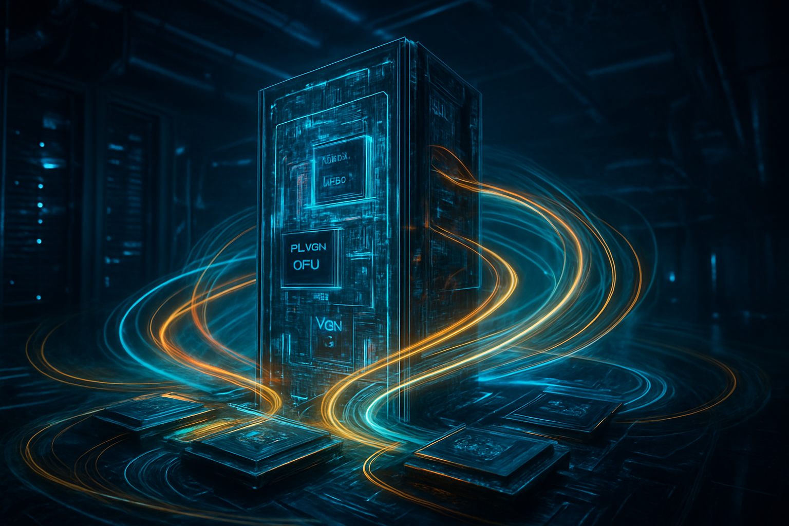
    The Technical Engine of Growth: HBM3e and the HBM4 Horizon

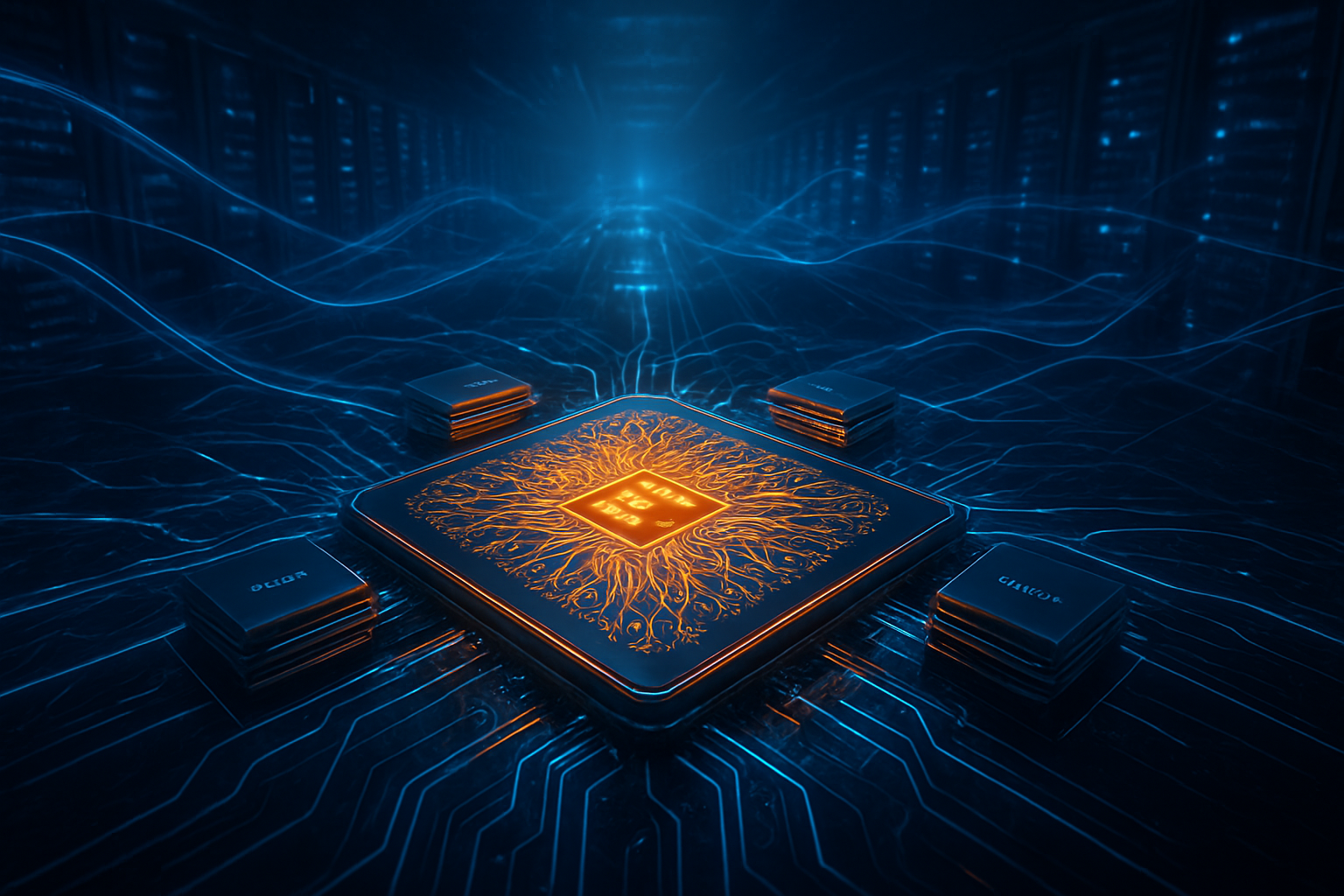
    The cornerstone of Samsung’s Q4 success was the rapid scaling of its Device Solutions (DS) Division. After navigating a challenging qualification process throughout 2025, Samsung successfully began mass shipments of its 12-layer HBM3e chips to Nvidia (NASDAQ:NVDA) for use in its Blackwell-series GPUs. These chips, which stack memory vertically to provide the massive bandwidth required for Large Language Model (LLM) training, saw a 400% increase in shipment volume over the previous quarter. Technical experts point to Samsung’s proprietary Advanced Thermal Compression Non-Conductive Film (TC-NCF) technology as a key differentiator, allowing for higher stack density and improved thermal management in the 12-layer configurations.

    Beyond HBM3e, the guidance highlights a significant shift in the broader memory market. Commodity DRAM prices for AI servers rose by nearly 50% in the final quarter of 2025, as demand for high-capacity DDR5 modules outpaced supply. Analysts from Susquehanna and KB Securities noted that the "AI Squeeze" is real: an AI server typically requires three to five times more memory than a standard enterprise server, and Samsung’s ability to leverage its massive "clean-room" capacity at the P4 facility in Pyeongtaek allowed it to capture market share that rivals SK Hynix (KRX:000660) and Micron (NASDAQ:MU) simply could not meet.

    Redefining the Competitive Landscape of the AI Era

    This earnings report sends a clear message to the Silicon Valley elite: Samsung is no longer playing catch-up. While SK Hynix held an early lead in the HBM market, Samsung’s sheer manufacturing scale and vertical integration are now shifting the balance of power. Major tech giants including Alphabet (NASDAQ:GOOGL), Meta (NASDAQ:META), and Microsoft (NASDAQ:MSFT) have reportedly signed multi-billion dollar long-term supply agreements with Samsung to insulate themselves from future shortages. These companies are building out "sovereign AI" and massive data center clusters that require millions of high-performance memory chips, making Samsung’s stability and volume a strategic asset.

    The competitive implications extend to the processor market as well. By securing reliable HBM supply from Samsung, AMD (NASDAQ:AMD) has been able to ramp up production of its MI300 and MI350-series accelerators, providing the first viable large-scale alternative to Nvidia’s dominance. For startups in the AI space, the increased supply from Samsung is a welcome relief, potentially lowering the barrier to entry for training smaller, specialized models as memory bottlenecks begin to ease at the mid-market level.

    A New Era for the Global Semiconductor Supply Chain

    The Q4 2025 results underscore a fundamental shift in the broader AI landscape. We are witnessing the decoupling of the semiconductor industry from its traditional reliance on consumer electronics. While Samsung’s Mobile Experience (MX) division saw compressed margins due to rising component costs, the explosive growth in the enterprise AI sector more than compensated for the shortfall. This suggests that the "AI Supercycle" is not merely a bubble, but a structural realignment of the global economy where high-compute infrastructure is the new gold.

    However, this rapid growth is not without its concerns. The concentration of the world’s most advanced memory production in a few facilities in South Korea remains a point of geopolitical tension. Furthermore, the "AI Squeeze" on commodity DRAM has led to price hikes for non-AI products, including laptops and gaming consoles, raising questions about inflationary pressures in the consumer tech sector. Comparisons are already being made to the 2000s internet boom, but experts argue that unlike the dot-com era, today’s growth is backed by tangible hardware sales and record-breaking profits rather than speculative valuations.

    Looking Ahead: The Race to HBM4 and 2nm

    The next frontier for Samsung is the transition to HBM4, which the company is slated to begin mass-producing in February 2026. This next generation of memory will integrate the logic die directly into the HBM stack, a move that requires unprecedented collaboration between memory designers and foundries. Samsung’s unique position as both a world-class memory maker and a leading foundry gives it a potential "one-stop-shop" advantage that competitors like SK Hynix—which must partner with TSMC—may find difficult to match.

    Looking further into 2026, industry watchers are focusing on Samsung’s implementation of Gate-All-Around (GAA) technology on its 2nm process. If Samsung can successfully pair its 2nm logic with its HBM4 memory, it could offer a complete AI "system-on-package" that significantly reduces power consumption and latency. This synergy is expected to be the primary battleground for 2026 and 2027, as AI models move toward "edge" devices like smartphones and robotics that require extreme efficiency.

    The Silicon Gold Rush Reaches Its Zenith

    Samsung’s record-breaking Q4 2025 guidance is a watershed moment in the history of artificial intelligence. By delivering a 20 trillion won operating profit, the company has proven that the massive investments in AI infrastructure are yielding immediate, tangible financial rewards. This performance marks the end of the "uncertainty phase" for AI memory and the beginning of a sustained period of infrastructure-led growth that will define the next decade of technology.

    As we move into the first quarter of 2026, investors and industry leaders should keep a close eye on the official earnings call later this month for specific details on HBM4 yields and 2nm customer wins. The primary takeaway is clear: the AI revolution is no longer just about software and algorithms—it is a battle of silicon, scale, and supply chains, and for the moment, Samsung is leading the charge.


    This content is intended for informational purposes only and represents analysis of current AI developments.

    TokenRing AI delivers enterprise-grade solutions for multi-agent AI workflow orchestration, AI-powered development tools, and seamless remote collaboration platforms.
    For more information, visit https://www.tokenring.ai/.

  • TSMC Unveils $250 Billion ‘Independent Gigafab Cluster’ in Arizona: A Massive Leap for AI Sovereignty

    TSMC Unveils $250 Billion ‘Independent Gigafab Cluster’ in Arizona: A Massive Leap for AI Sovereignty

    In a move that fundamentally reshapes the global technology landscape, Taiwan Semiconductor Manufacturing Company (NYSE:TSM) has announced a monumental expansion of its operations in the United States. Following the acquisition of a 901-acre plot of land in North Phoenix, the company has unveiled plans to develop an "independent gigafab cluster." This expansion is the cornerstone of a historic $250 billion technology trade agreement between the U.S. and Taiwan, aimed at securing the supply chain for the most advanced artificial intelligence and consumer electronics components on the planet.

    This development marks a pivot from regional manufacturing to a self-sufficient "megacity" of silicon. By late 2025 and early 2026, the Arizona site has evolved from a satellite facility into a strategic titan, intended to house up to a dozen individual fabrication plants (fabs). With lead customers like NVIDIA (NASDAQ:NVDA) and Apple (NASDAQ:AAPL) already queuing for capacity, the Phoenix complex is positioned to become the primary engine for the next decade of AI innovation, producing the sub-2nm chips that will power everything from autonomous agents to the next generation of data centers.

    Engineering the Gigafab: A Technical Leap into the Angstrom Era

    The technical specifications of the new Arizona cluster represent the bleeding edge of semiconductor physics. The 901-acre acquisition nearly doubles TSMC’s physical footprint in the region, providing the space necessary for "Gigafabs"—facilities capable of producing over 100,000 12-inch wafers per month. Unlike earlier iterations of the Arizona project which trailed Taiwan's "mother fabs" by several years, this new cluster is designed for "process parity." By 2027, the site will transition from 4nm and 3nm production to the highly anticipated 2nm (N2) node, featuring Gate-All-Around (GAAFET) transistor architecture.

    The most significant technical milestone, however, is the integration of the A16 (1.6nm) process node. Slated for the late 2020s in Arizona, the A16 node introduces Super Power Rail (SPR) technology. This breakthrough moves the power delivery network to the backside of the wafer, separate from the signal routing on the front. This architectural shift addresses the "power wall" that has hindered AI chip scaling, offering an estimated 10% increase in clock speeds and a 20% reduction in power consumption compared to the 2nm process.

    Industry experts note that this "independent cluster" strategy differs from previous approaches by including on-site advanced packaging facilities. Previously, wafers produced in the U.S. had to be shipped back to Asia for Chip-on-Wafer-on-Substrate (CoWoS) packaging. The new Arizona roadmap integrates these "back-end" processes directly into the Phoenix site, creating a closed-loop manufacturing ecosystem that slashes logistics lead times and protects sensitive IP from the risks of trans-Pacific transit.

    The AI Titans Stake Their Claim: Apple, NVIDIA, and the New Market Dynamic

    The expansion is a direct response to the insatiable demand from the "AI Titans." NVIDIA has emerged as a primary beneficiary, reportedly securing the lead customer position for the Arizona A16 capacity. This will support their upcoming "Feynman" GPU architecture, the successor to the Blackwell and Rubin series, which requires unprecedented transistor density to manage the trillions of parameters in future Large Language Models (LLMs). For NVIDIA, having a massive, reliable source of silicon on U.S. soil mitigates geopolitical risks and stabilizes its dominant market position in the data center sector.

    Apple also remains a central figure in the Arizona strategy. The tech giant has already moved to secure over 50% of the initial 2nm capacity in the Phoenix cluster for its A-series and M-series chips. This ensures that the iPhone 18 and future MacBook Pros will be "Made in America" at the silicon level, a significant strategic advantage for Apple as it navigates global trade tensions and consumer demand for domestic manufacturing. The proximity of the fabs to Apple's design centers in the U.S. allows for tighter integration between hardware and software development.

    This $250 billion influx places immense pressure on competitors like Intel (NASDAQ:INTC) and Samsung (KRX:005930). While Intel has pursued a "Foundry 2.0" strategy with its own massive investments in Ohio and Arizona, TSMC's "Gigafab" scale and proven yield rates present a formidable challenge. For startups and mid-tier AI labs, the existence of a massive domestic foundry could lower the barriers to entry for custom silicon (ASICs), as TSMC looks to fill its dozen planned fabs with a diverse array of clients beyond just the trillion-dollar giants.

    Geopolitical Resilience and the Global AI Landscape

    The broader significance of the $250 billion trade deal cannot be overstated. By incentivizing TSMC to build 12 fabs in Arizona, the U.S. government is effectively creating a "silicon shield" that is geographical rather than purely political. This shift addresses the "single point of failure" concern that has haunted the tech industry for years: the concentration of 90% of advanced logic chips in a single, geopolitically sensitive island. The deal includes a 5% reduction in baseline tariffs for Taiwanese goods and massive credit guarantees, signaling a deep, long-term entanglement between the U.S. and Taiwan's economies.

    However, the expansion is not without its critics and concerns. Environmental advocates point to the massive water and energy requirements of a 12-fab cluster in the arid Arizona desert. While TSMC has committed to near-100% water reclamation and the use of renewable energy, the sheer scale of the "Gigafab" cluster will test the state's infrastructure. Furthermore, the reliance on a single foreign entity for domestic AI sovereignty raises questions about long-term independence, even if the factories are physically located in Phoenix.

    This milestone is frequently compared to the 1950s "Space Race," but with transistors instead of rockets. Just as the Apollo program spurred a generation of American innovation, the Arizona Gigafab cluster is expected to foster a local ecosystem of suppliers, researchers, and engineers. The "independent" nature of the site means that for the first time, the entire lifecycle of a chip—from design to wafer to packaging—can happen within a 50-mile radius in the United States.

    The Road Ahead: Workforce, Water, and 1.6nm

    Looking toward the late 2020s, the primary challenge for the Arizona expansion will be the human element. Managing a dozen fabs requires a workforce of tens of thousands of specialized engineers and technicians. TSMC has already begun partnering with local universities and technical colleges, but the "war for talent" between TSMC, Intel, and the surging AI startup sector remains a critical bottleneck. Near-term developments will likely focus on the completion of Fabs 4 through 6, with the first 2nm test runs expected by early 2027.

    In the long term, we expect to see the Phoenix cluster move beyond traditional logic chips into specialized AI accelerators and photonics. As AI models move toward "physical world" applications like humanoid robotics and real-time edge processing, the low-latency benefits of domestic manufacturing will become even more pronounced. Experts predict that if the 12-fab goal is reached by 2030, Arizona will rival Taiwan’s Hsinchu Science Park as the most important plot of land in the digital world.

    A New Chapter in Industrial History

    The transformation of 901 acres of Arizona desert into a $250 billion silicon fortress marks a definitive chapter in the history of artificial intelligence. It is the moment when the "cloud" became grounded in physical, domestic infrastructure of an unprecedented scale. By moving its most advanced processes—2nm, A16, and beyond—to the United States, TSMC is not just building factories; it is anchoring the future of the AI economy to American soil.

    As we look forward into 2026 and beyond, the success of this "independent gigafab cluster" will be measured not just in wafer starts, but in its ability to sustain the rapid pace of AI evolution. For investors, tech enthusiasts, and policymakers, the Phoenix complex is the place to watch. The chips that will define the next decade are being forged in the Arizona heat, and the stakes have never been higher.


    This content is intended for informational purposes only and represents analysis of current AI developments.

    TokenRing AI delivers enterprise-grade solutions for multi-agent AI workflow orchestration, AI-powered development tools, and seamless remote collaboration platforms.
    For more information, visit https://www.tokenring.ai/.

  • The Dawn of the Rubin Era: NVIDIA’s Six-Chip Architecture Promises to Slash AI Costs by 10x

    The Dawn of the Rubin Era: NVIDIA’s Six-Chip Architecture Promises to Slash AI Costs by 10x

    At the opening keynote of CES 2026 in Las Vegas, NVIDIA (NASDAQ: NVDA) CEO Jensen Huang stood before a packed audience to unveil the Rubin architecture, a technological leap that signals the end of the "Blackwell" era and the beginning of a new epoch in accelerated computing. Named after the pioneering astronomer Vera Rubin, the new platform is not merely a faster graphics processor; it is a meticulously "extreme-codesigned" ecosystem intended to serve as the foundational bedrock for the next generation of agentic AI and trillion-parameter reasoning models.

    The announcement sent shockwaves through the industry, primarily due to NVIDIA’s bold claim that the Rubin platform will reduce AI inference token costs by a staggering 10x. By integrating compute, networking, and memory into a unified "AI factory" design, NVIDIA aims to make persistent, always-on AI agents economically viable for the first time, effectively democratizing high-level intelligence at a scale previously thought impossible.

    The Six-Chip Symphony: Technical Specs of the Rubin Platform

    The heart of this announcement is the transition from a GPU-centric model to a comprehensive "six-chip" unified platform. Central to this is the Rubin GPU (R200), a dual-die behemoth boasting 336 billion transistors—a 1.6x increase in density over its predecessor. This silicon giant delivers 50 Petaflops of NVFP4 compute performance. Complementing the GPU is the newly christened Vera CPU, NVIDIA’s first dedicated high-performance processor designed specifically for AI orchestration. Built on 88 custom "Olympus" ARM cores (v9.2-A), the Vera CPU utilizes spatial multi-threading to handle 176 concurrent threads, ensuring that the Rubin GPUs are never starved for data.

    To solve the perennial "memory wall" bottleneck, NVIDIA has fully embraced HBM4 memory. Each Rubin GPU features 288GB of HBM4, delivering an unprecedented 22 TB/s of memory bandwidth—a 2.8x jump over the Blackwell generation. This is coupled with the NVLink-C2C (Chip-to-Chip) interconnect, providing 1.8 TB/s of coherent bandwidth between the Vera CPU and Rubin GPUs. Rounding out the six-chip platform are the NVLink 6 Switch, the ConnectX-9 SuperNIC, the BlueField-4 DPU, and the Spectrum-6 Ethernet Switch, all designed to work in concert to eliminate latency in million-GPU clusters.

    The technical community has responded with a mix of awe and strategic caution. While the 3rd-generation Transformer Engine's hardware-accelerated adaptive compression is being hailed as a "game-changer" for Mixture-of-Experts (MoE) models, some researchers note that the sheer complexity of the rack-scale architecture will require a complete rethink of data center cooling and power delivery. The Rubin platform moves liquid cooling from an optional luxury to a mandatory standard, as the power density of these "AI factories" reaches new heights.

    Disruption in the Datacenter: Impact on Tech Giants and Competitors

    The unveiling of Rubin has immediate and profound implications for the world’s largest technology companies. Hyperscalers such as Microsoft (NASDAQ: MSFT), Alphabet (NASDAQ: GOOGL), and Amazon (NASDAQ: AMZN) have already announced massive procurement orders, with Microsoft’s upcoming "Fairwater" superfactories expected to be the first to deploy the Vera Rubin NVL72 rack systems. For these giants, the promised 10x reduction in inference costs is the key to moving their AI services from loss-leading experimental features to highly profitable enterprise utilities.

    For competitors like Advanced Micro Devices (NASDAQ: AMD), the Rubin announcement raises the stakes significantly. Industry analysts noted that NVIDIA’s decision to upgrade Rubin's memory bandwidth to 22 TB/s shortly before the CES reveal was a tactical maneuver to overshadow AMD’s Instinct MI455X. By offering a unified CPU-GPU-Networking stack, NVIDIA is increasingly positioning itself not just as a chip vendor, but as a vertically integrated platform provider, making it harder for "best-of-breed" component strategies from rivals to gain traction in the enterprise market.

    Furthermore, AI research labs like OpenAI and Anthropic are viewing Rubin as the necessary hardware "step-change" to enable agentic AI. OpenAI CEO Sam Altman, who made a guest appearance during the keynote, emphasized that the efficiency gains of Rubin are essential for scaling models that can perform long-context reasoning and maintain "memory" over weeks or months of user interaction. The strategic advantage for any lab securing early access to Rubin silicon in late 2026 could be the difference between a static chatbot and a truly autonomous digital employee.

    Sustainability and the Evolution of the AI Landscape

    Beyond the raw performance metrics, the Rubin architecture addresses the growing global concern regarding the energy consumption of AI. NVIDIA claims an 8x improvement in performance-per-watt over previous generations. This shift is critical as the world grapples with the power demands of the "AI revolution." By requiring 4x fewer GPUs to train the same MoE models compared to the Blackwell architecture, Rubin offers a path toward a more sustainable, if still power-hungry, future for digital intelligence.

    The move toward "agentic AI"—systems that can plan, reason, and execute complex tasks over long periods—is the primary trend driving this hardware evolution. Previously, the cost of keeping a high-reasoning model "active" for hours of thought was prohibitive. With Rubin, the cost per token drops so significantly that these "thinking" models can become ubiquitous. This follows the broader industry trend of moving away from simple prompt-response interactions toward continuous, collaborative AI workflows.

    However, the rapid pace of development has also sparked concerns about "hardware churn." With Blackwell only reaching volume production six months ago, the announcement of its successor has some enterprise buyers worried about the rapid depreciation of their current investments. NVIDIA’s aggressive roadmap—which includes a "Rubin Ultra" refresh already slated for 2027—suggests that the window for "cutting-edge" hardware is shrinking to a matter of months, forcing a cycle of constant reinvestment for those who wish to remain competitive in the AI arms race.

    Looking Ahead: The Road to Late 2026 and Beyond

    While the CES 2026 announcement provided the blueprint, the actual market rollout of the Rubin platform is scheduled for the second half of 2026. This timeline gives cloud providers and enterprises roughly nine months to prepare their infrastructure for the transition to HBM4 and the Vera CPU's ARM-based orchestration. In the near term, we can expect a flurry of software updates to CUDA and other NVIDIA libraries as the company prepares developers to take full advantage of the new NVLink 6 and 3rd-gen Transformer Engine.

    The long-term vision teased by Jensen Huang points toward the "Kyber" architecture in 2028, which is rumored to push rack-scale performance to 600kW. For now, the focus remains on the successful manufacturing of the Rubin R200 GPU. The complexity of the dual-die design and the integration of HBM4 will be the primary hurdles for NVIDIA’s supply chain. If successful, the Rubin architecture will likely be remembered as the moment AI hardware finally caught up to the ambitious dreams of software researchers, providing the raw power needed for truly autonomous intelligence.

    Summary of a Landmark Announcement

    The unveiling of the NVIDIA Rubin architecture at CES 2026 marks a definitive moment in tech history. By promising a 10x reduction in inference costs and delivering a tightly integrated six-chip platform, NVIDIA has consolidated its lead in the AI infrastructure market. The combination of the Vera CPU, the Rubin GPU, and HBM4 memory represents a fundamental redesign of how computers think, prioritizing the flow of data and the efficiency of reasoning over simple raw compute.

    As we move toward the late 2026 launch, the industry will be watching closely to see if NVIDIA can meet its ambitious production targets and if the 10x cost reduction translates into a new wave of AI-driven economic productivity. For now, the "Rubin Era" has officially begun, and the stakes for the future of artificial intelligence have never been higher.


    This content is intended for informational purposes only and represents analysis of current AI developments.

    TokenRing AI delivers enterprise-grade solutions for multi-agent AI workflow orchestration, AI-powered development tools, and seamless remote collaboration platforms.
    For more information, visit https://www.tokenring.ai/.

  • The Silicon Pact: US and Taiwan Ink $500 Billion Landmark Trade Deal to Secure AI Future

    The Silicon Pact: US and Taiwan Ink $500 Billion Landmark Trade Deal to Secure AI Future

    In a move that fundamentally reshapes the global technology landscape, the United States and Taiwan signed a historic trade agreement on January 15, 2026, officially known as the "Silicon Pact." This sweeping deal secures a massive $250 billion commitment from leading Taiwanese technology firms to expand their footprint in the U.S., matched by $250 billion in credit guarantees from the American government. The primary objective is the creation of a vertically integrated, "full-stack" semiconductor supply chain within North America, effectively shielding the critical infrastructure required for the artificial intelligence revolution from geopolitical volatility.

    The signing of the agreement marks the end of a decades-long reliance on offshore manufacturing for the world’s most advanced processors. By establishing a domestic ecosystem that includes everything from raw wafer production to advanced lithography and chemical processing, the U.S. aims to decouple its AI future from vulnerable overseas routes. Immediate market reaction was swift, with semiconductor indices surging as the pact also included a strategic reduction of baseline tariffs on Taiwanese imports from 20% to 15%, providing an instant financial boost to the hardware companies fueling the generative AI boom.

    Technical Infrastructure: Beyond the Fab to a Full Supply Chain

    The technical backbone of the deal centers on the rapid expansion of "megafab" clusters, primarily in Arizona and Texas. Taiwan Semiconductor Manufacturing Co. (NYSE: TSM), the linchpin of the pact, has committed to expanding its initial three-fab roadmap to a staggering 11-fab complex by 2030. This expansion isn't just about quantity; it brings the world’s first domestic 2-nanometer (2nm) and sub-2nm mass production lines to U.S. soil. Unlike previous initiatives that focused solely on logic chips, this agreement includes the entire ecosystem: GlobalWafers (TPE: 6488) is scaling its 300mm silicon wafer plant in Texas, while Chang Chun Group and Sunlit Chemical are building specialized facilities to provide the electronic-grade chemicals required for high-NA EUV lithography.

    A critical, often overlooked component of the pact is the commitment to advanced packaging. For years, "Made in America" chips still had to be shipped back to Asia for the complex assembly required for high-performance AI chips like those from NVIDIA (NASDAQ: NVDA). Under the new deal, a network of domestic packaging centers will be established in collaboration with firms like Amkor and Hon Hai Technology Group (Foxconn) (TPE: 2317). This technical integration ensures that the "latency of the ocean" is removed from the supply chain, allowing for a 30% faster turnaround from silicon design to data center deployment. Industry experts note that this represents the first time a major manufacturing nation has attempted to replicate the high-density industrial "clustering" effect of Hsinchu, Taiwan, within the vast geography of the United States.

    Industry Impact: Bridging the Software-Hardware Divide

    The implications for the technology industry are profound, creating a "two-tier" market where participants in the Silicon Pact gain significant strategic advantages. Cloud hyperscalers like Microsoft (NASDAQ: MSFT), Amazon (NASDAQ: AMZN), and Alphabet (NASDAQ: GOOGL) are expected to be the immediate beneficiaries, as the domestic supply chain will offer them first-access to "sovereign" AI hardware that meets the highest security standards. Meanwhile, Intel (NASDAQ: INTC) stands to gain through enhanced cross-border collaboration, as the pact encourages joint ventures between Intel Foundry and Taiwanese designers like MediaTek (TPE: 2454), who are increasingly moving their mobile and AI edge-device production to U.S.-based nodes.

    For consumer tech giants, the deal provides a long-awaited hedge against supply shocks. Apple (NASDAQ: AAPL), which has long been TSMC’s largest customer, will see its high-end iPhone and Mac processors manufactured entirely within the U.S. by 2027. The competitive landscape will likely see a shift where "hardware-software co-design" becomes more localized. Startups specializing in niche AI applications will also benefit from the $250 billion in credit guarantees, which are specifically designed to help smaller tier-two and tier-three suppliers move their operations to the new American tech hubs, ensuring that the supply chain isn't just a collection of giant fabs, but a robust network of specialized innovators.

    Geopolitical Significance and the "Silicon Shield"

    Beyond the immediate economic figures, the US-Taiwan deal signals a broader shift toward "Sovereign AI." In a world where compute power has become synonymous with national power, the ability to produce advanced semiconductors is no longer just a business interest—it is a national security imperative. The reduction of tariffs from 20% to 15% is a deliberate diplomatic lever, effectively rewarding Taiwan for its cooperation while creating a "Silicon Shield" that integrates the two economies more tightly than ever before. This move is a clear response to the global trend of "onshoring," mirroring similar moves by the European Union and Japan to secure their own technological autonomy.

    However, the scale of this commitment has raised concerns regarding environmental and labor impacts. Building 11 mega-fabs in a water-stressed state like Arizona requires unprecedented investments in water reclamation and renewable energy infrastructure. The $250 billion in U.S. credit guarantees, largely funneled through the Department of Energy’s loan programs, are intended to address this by funding massive clean-energy projects to power these power-hungry facilities. Comparisons are already being drawn to the historic breakthroughs of the 1950s aerospace era; this is the "Apollo Program" of the AI age, a massive state-supported push to ensure the digital foundation of the next century remains stable.

    The Road Ahead: 2nm Nodes and the Infrastructure of 2030

    Looking ahead, the near-term focus will be on the construction "gold rush" in the Southwest. By mid-2026, the first wave of specialized Taiwanese suppliers is expected to break ground on over 40 new facilities. The real test of the pact will come in 2027 and 2028, as the first 2nm chips roll off the assembly lines. We are also likely to see the emergence of "AI Economic Zones" in Texas and Arizona, where local universities and tech firms receive targeted funding to develop the talent pool required to manage these highly automated facilities.

    Experts predict that the next phase of this trade relationship will focus on "next-gen" materials beyond silicon, such as gallium nitride and silicon carbide for power electronics. Challenges remain, particularly in workforce development and the potential for regulatory bottlenecks. If the U.S. cannot streamline its permitting processes for these high-tech zones, the massive financial commitments could face delays. However, the sheer scale of the $500 billion framework suggests a political and corporate will that is unlikely to be deterred by bureaucratic hurdles.

    Summary: A New Era for the AI Economy

    The signing of the US-Taiwan trade deal on January 15, 2026, will be remembered as the moment the AI era transitioned from a software race to a physical infrastructure reality. By committing half a trillion dollars in combined private and public resources, the two nations have laid a foundation for decades of technological growth. The key takeaway for the industry is clear: the future of high-performance computing is moving home, and the era of the "globalized-but-fragile" supply chain is coming to a close.

    As the industry watches these developments, the focus over the coming months will shift to the implementation phase. Investors will be looking for quarterly updates on construction milestones and the first signs of the "clustering effect" taking hold. This development doesn't just represent a new chapter in trade; it defines the infrastructure of the 21st century.


    This content is intended for informational purposes only and represents analysis of current AI developments.

    TokenRing AI delivers enterprise-grade solutions for multi-agent AI workflow orchestration, AI-powered development tools, and seamless remote collaboration platforms.
    For more information, visit https://www.tokenring.ai/.

  • The 3nm Silicon Hunger Games: Tech Titans Clash Over TSMC’s Finite 2026 Capacity

    The 3nm Silicon Hunger Games: Tech Titans Clash Over TSMC’s Finite 2026 Capacity

    TAIPEI, TAIWAN – As of January 22, 2026, the global artificial intelligence race has reached a fever pitch, shifting from a battle over software algorithms to a brutal competition for physical silicon. At the center of this storm is Taiwan Semiconductor Manufacturing Company (TSMC) (NYSE: TSM), whose 3-nanometer (3nm) production lines are currently operating at a staggering 100% capacity. With high-performance computing (HPC) and generative AI demand scaling exponentially, industry leaders like NVIDIA, AMD, and Tesla are engaged in a high-stakes "Silicon Hunger Games," jockeying for priority as the N3P process node becomes the de facto standard for the world’s most powerful chips.

    The significance of this bottleneck cannot be overstated. In early 2026, wafer starts have replaced venture capital as the primary currency of the AI industry. For the first time in history, NVIDIA (NASDAQ: NVDA) has officially surpassed Apple Inc. (NASDAQ: AAPL) as TSMC’s largest customer by revenue, a symbolic passing of the torch from the mobile era to the age of the AI data center. As the industry grapples with the physical limits of Moore’s Law, the competition for 3nm supply is no longer just about who has the best design, but who has secured the most floor space in the world’s most advanced cleanrooms.

    Engineering the 2026 AI Infrastructure

    The 3nm family of nodes, specifically the N3P (Performance) and N3X (Extreme) variants, represents a monumental leap over the 5nm nodes that powered the first wave of the generative AI boom. In 2026, the N3P node has emerged as the industry’s "workhorse," offering a 5% performance increase or a 10% reduction in power consumption compared to the earlier N3E process. More importantly, it provides the transistor density required to integrate the next generation of High Bandwidth Memory, HBM4, which is essential for training the trillion-parameter models now entering the market.

    NVIDIA’s new Rubin architecture, spearheaded by the R100 GPU, is the primary driver of this technical shift. Unlike its predecessor, Blackwell, the Rubin series is the first to fully embrace a modular "chiplet" design on 3nm, integrating eight stacks of HBM4 to achieve a record-breaking 22.2 TB/s of memory bandwidth. Meanwhile, the specialized N3X node is catering to the "Ultra-HPC" segment, allowing for higher voltage tolerances that enable chips to reach peak clock speeds previously thought impossible at such small scales. Industry experts note that while the shift to 3nm has been technically grueling, the stabilization of yield rates at roughly 70% for these complex designs has allowed mass production to finally keep pace—barely—with global demand.

    A Four-Way Battle for Dominance

    The competitive landscape of 2026 is defined by four distinct strategies. NVIDIA (NASDAQ: NVDA) has secured the lion's share of TSMC's N3P capacity through massive pre-payments, ensuring that its Rubin-based systems dominate the enterprise sector. However, Advanced Micro Devices (NASDAQ: AMD) is not backing down. AMD is reportedly utilizing a "leapfrog" strategy, employing a mix of 3nm and early 2nm (N2) chiplets for its Instinct MI450 series. This hybrid approach allows AMD to offer higher memory capacities—up to 432GB of HBM4—challenging NVIDIA’s dominance in large-scale inference tasks.

    Tesla, Inc. (NASDAQ: TSLA) has also emerged as a top-tier silicon player. CEO Elon Musk confirmed this month that Tesla's AI-5 (Hardware 5) chip has entered mass production on the N3P node. Designed specifically for the rigorous demands of unsupervised Full Self-Driving (FSD) and the Optimus robotics line, the AI-5 delivers 2,500 TOPS (Tera Operations Per Second), a 5x increase over previous 5nm iterations. Simultaneously, Apple Inc. (NASDAQ: AAPL) continues to consume significant 3nm volume for its M5-series chips, though it has begun shifting its flagship iPhone processors to 2nm to maintain a consumer-side advantage. This multi-front demand has created a "sold-out" status for TSMC through at least the third quarter of 2026.

    The Chiplet Revolution and the Death of the Monolithic Die

    The intensity of the 3nm competition is inextricably linked to the 'Chiplet Revolution.' As transistors approach atomic scales, manufacturing a single, massive "monolithic" chip has become economically and physically unviable. In 2026, the industry has hit the "Reticle Limit"—the maximum size a single chip can be printed—forcing a shift toward Advanced Packaging. Technologies like TSMC’s CoWoS-L (Chip-on-Wafer-on-Substrate with Local Interconnect) have become the bottleneck of 2026, with packaging capacity being just as scarce as the 3nm wafers themselves.

    This shift has been standardized by the widespread adoption of UCIe 3.0 (Universal Chiplet Interconnect Express). This protocol allows chiplets from different vendors to communicate with the same speed as if they were on the same piece of silicon. This modularity is a strategic advantage for companies like Intel Corporation (NASDAQ: INTC), which is now using its Foveros Direct 3D packaging to stack 3nm compute tiles from TSMC on top of its own power-delivery base layers. By breaking one large chip into several smaller chiplets, manufacturers have significantly improved yields, as a single defect now only ruins a small fraction of the total silicon rather than the entire processor.

    The Road to 2nm and Backside Power

    Looking toward the horizon of late 2026 and 2027, the focus is already shifting to the next frontier: the N2 (2-nanometer) node and the introduction of Backside Power Delivery (BSPD). Experts predict that while 3nm will remain the high-volume standard for the next 18 months, the elite "Tier-1" AI players are already bidding for 2nm pilot lines. The transition to Nano-sheet transistors at 2nm will offer another 15% performance jump, but at a cost that may exclude all but the largest tech conglomerates.

    Furthermore, the emergence of OpenAI as a custom silicon designer is a trend to watch. Rumors of their "Titan" chip, slated for late 2026 on a mix of 3nm and 2nm nodes, suggest that the software-hardware vertical integration seen at Apple and Tesla is becoming the blueprint for all major AI labs. The primary challenge moving forward will be the "Power Wall"—as chips become denser and more powerful, the energy required to run and cool them is exceeding the capacity of traditional data center infrastructure, necessitating a mandatory shift to liquid-to-chip cooling.

    TSMC as the Global Kingmaker

    As we move further into 2026, it is clear that TSMC (NYSE: TSM) has cemented its position as the ultimate kingmaker of the AI era. The intense competition for 3nm wafer supply between NVIDIA, AMD, and Tesla highlights a fundamental truth: in the world of artificial intelligence, physical manufacturing capacity is the ultimate constraint. The successful transition to chiplet-based architectures has saved Moore’s Law from a premature end, but it has also added a new layer of complexity to the supply chain through advanced packaging requirements.

    The key takeaways for the coming months are the stabilization of Rubin-class GPU shipments and the potential entry of "commercial chiplets," where companies may begin selling specialized AI accelerators that can be integrated into custom third-party packages. For investors and industry watchers, the metrics to follow are no longer just quarterly earnings, but TSMC’s monthly CoWoS output and the progress of the N2 ramp-up. The silicon war is far from over, but in early 2026, the 3nm node is the hill that every tech giant is fighting to occupy.


    This content is intended for informational purposes only and represents analysis of current AI developments.

    TokenRing AI delivers enterprise-grade solutions for multi-agent AI workflow orchestration, AI-powered development tools, and seamless remote collaboration platforms.
    For more information, visit https://www.tokenring.ai/.

  • The Custom Silicon Gold Rush: How Broadcom and the ‘Cloud Titans’ are Challenging Nvidia’s AI Dominance

    The Custom Silicon Gold Rush: How Broadcom and the ‘Cloud Titans’ are Challenging Nvidia’s AI Dominance

    As of January 22, 2026, the artificial intelligence industry has reached a pivotal inflection point, shifting from a mad scramble for general-purpose hardware to a sophisticated era of architectural vertical integration. Broadcom (NASDAQ: AVGO), long the silent architect of the internet’s backbone, has emerged as the primary beneficiary of this transition. In its latest fiscal report, the company revealed a staggering $73 billion AI-specific order backlog, signaling that the world’s largest tech companies—Google (NASDAQ: GOOGL), Meta (NASDAQ: META), and now OpenAI—are increasingly bypassing traditional GPU vendors in favor of custom-tailored silicon.

    This surge in custom "XPUs" (AI accelerators) marks a fundamental change in the economics of the cloud. By partnering with Broadcom to design application-specific integrated circuits (ASICs), the "Cloud Titans" are achieving performance-per-dollar metrics that were previously unthinkable. This development not only threatens the absolute dominance of the general-purpose GPU but also suggests that the next phase of the AI race will be won by those who own their entire hardware and software stack.

    Custom XPUs: The Technical Blueprint of the Million-Accelerator Era

    The technical centerpiece of this shift is the arrival of seventh and eighth-generation custom accelerators. Google’s TPU v7, codenamed "Ironwood," which entered mass deployment in late 2025, has set a new benchmark for efficiency. By optimizing the silicon specifically for Google’s internal software frameworks like JAX and XLA, Broadcom and Google have achieved a 70% reduction in cost-per-token compared to the previous generation. This leap puts custom silicon at parity with, and in some specific training workloads, ahead of Nvidia’s (NASDAQ: NVDA) Blackwell architecture.

    Beyond the compute cores themselves, Broadcom is solving the "interconnect bottleneck" that has historically limited AI scaling. The introduction of the Tomahawk 6 (Davisson) switch—the industry’s first 102.4 Terabits per second (Tbps) single-chip Ethernet switch—allows for the creation of "flat" network topologies. This enables hyperscalers to link up to one million XPUs in a single, cohesive fabric. In early 2026, this "Million-XPU" cluster capability has become the new standard for training the next generation of Frontier Models, which now require compute power measured in gigawatts rather than megawatts.

    A critical technical differentiator for Broadcom is its 3rd-generation Co-Packaged Optics (CPO) technology. As AI power demands reach nearly 200kW per server rack, traditional pluggable optical modules have become a primary source of heat and energy waste. Broadcom’s CPO integrates optical interconnects directly onto the chip package, reducing power consumption for data movement by 30-40%. This integration is essential for the 3nm and upcoming 2nm production nodes, where thermal management is as much of a constraint as transistor density.

    Industry experts note that this move toward ASICs represents a "de-generalization" of AI hardware. While Nvidia’s H100 and B200 series are designed to run any model for any customer, custom silicon like Meta’s MTIA (Meta Training and Inference Accelerator) is stripped of unnecessary components. This leaner design allows for more area on the die to be dedicated to high-bandwidth memory (HBM3e and HBM4) and specialized matrix-math units, specifically tuned for the recommendation algorithms and Large Language Models (LLMs) that drive Meta’s core business.

    Market Shift: The Rise of the ASIC Alliances

    The financial implications of this shift are profound. Broadcom’s AI-related semiconductor revenue hit $6.5 billion in the final quarter of 2025, a 74% year-over-year increase, with guidance for Q1 2026 suggesting a jump to $8.2 billion. This trajectory has repositioned Broadcom not just as a component supplier, but as a strategic peer to the world's most valuable companies. The company’s shift toward selling complete "AI server racks"—inclusive of custom silicon, high-speed switches, and integrated optics—has increased the total dollar value of its customer engagements ten-fold.

    Meta has particularly leaned into this strategy through its "Project Santa Barbara" rollout in early 2026. By doubling its in-house chip capacity using Broadcom-designed silicon, Meta is significantly reducing its "Nvidia tax"—the premium paid for general-purpose flexibility. For Meta and Google, every dollar saved on hardware procurement is a dollar that can be reinvested into data acquisition and model training. This vertical integration provides a massive strategic advantage, allowing these giants to offer AI services at lower price points than competitors who rely solely on off-the-shelf components.

    Nvidia, while still the undisputed leader in the broader enterprise and startup markets due to its dominant CUDA software ecosystem, is facing a narrowing "moat" at the very top of the market. The "Big 5" hyperscalers, which account for a massive portion of Nvidia's revenue, are bifurcating their fleets: using Nvidia for third-party cloud customers who require the flexibility of CUDA, while shifting their own massive internal workloads to custom Broadcom-assisted silicon. This trend is further evidenced by Amazon (NASDAQ: AMZN), which continues to iterate on its Trainium and Inferentia lines, and Microsoft (NASDAQ: MSFT), which is now deploying its Maia 200 series across its Azure Copilot services.

    Perhaps the most disruptive announcement of the current cycle is the tripartite alliance between Broadcom, OpenAI, and various infrastructure partners to develop "Titan," a custom AI accelerator designed to power a 10-gigawatt computing initiative. This move by OpenAI signals that even the premier AI research labs now view custom silicon as a prerequisite for achieving Artificial General Intelligence (AGI). By moving away from general-purpose hardware, OpenAI aims to gain direct control over the hardware-software interface, optimizing for the unique inference requirements of its most advanced models.

    The Broader AI Landscape: Verticalization as the New Standard

    The boom in custom silicon reflects a broader trend in the AI landscape: the transition from the "exploration phase" to the "optimization phase." In 2023 and 2024, the goal was simply to acquire as much compute as possible, regardless of cost. In 2026, the focus has shifted to efficiency, sustainability, and total cost of ownership (TCO). This move toward verticalization mirrors the historical evolution of the smartphone industry, where Apple’s move to its own A-series and M-series silicon allowed it to outpace competitors who relied on generic chips.

    However, this trend also raises concerns about market fragmentation. As each tech giant develops its own proprietary hardware and optimized software stack (such as Google’s XLA or Meta’s PyTorch-on-MTIA), the AI ecosystem could become increasingly siloed. For developers, this means that a model optimized for AWS’s Trainium may not perform identically on Google’s TPU or Microsoft’s Maia, potentially complicating the landscape for multi-cloud AI deployments.

    Despite these concerns, the environmental impact of custom silicon cannot be overlooked. General-purpose GPUs are, by definition, less efficient than specialized ASICs for specific tasks. By stripping away the "dark silicon" that isn't used for AI training and inference, and by utilizing Broadcom's co-packaged optics, the industry is finding a path toward scaling AI without a linear increase in carbon footprint. The "performance-per-watt" metric has replaced raw TFLOPS as the most critical KPI for data center operators in 2026.

    This milestone also highlights the critical role of the semiconductor supply chain. While Broadcom designs the architecture, the entire ecosystem remains dependent on TSMC’s advanced nodes. The fierce competition for 3nm and 2nm capacity has turned the semiconductor foundry into the ultimate geopolitical and economic chokepoint. Broadcom’s success is largely due to its ability to secure massive capacity at TSMC, effectively acting as an aggregator of demand for the world’s largest tech companies.

    Future Horizons: The 2nm Era and Beyond

    Looking ahead, the roadmap for custom silicon is increasingly ambitious. Broadcom has already secured significant capacity for the 2nm production node, with initial designs for "TPU v9" and "Titan 2" expected to tape out in late 2026. These next-generation chips will likely integrate even more advanced memory technologies, such as HBM4, and move toward "chiplet" architectures that allow for even greater customization and yield efficiency.

    In the near term, we expect to see the "Million-XPU" clusters move from experimental projects to the backbone of global AI infrastructure. The challenge will shift from designing the chips to managing the staggering power and cooling requirements of these mega-facilities. Liquid cooling and on-chip thermal management will become standard features of any Broadcom-designed system by 2027. We may also see the rise of "Edge-ASICs," as companies like Meta and Google look to bring custom AI acceleration to consumer devices, further integrating Broadcom's IP into the daily lives of billions.

    Experts predict that the next major hurdle will be the "IO Wall"—the speed at which data can be moved between chips. While Tomahawk 6 and CPO have provided a temporary reprieve, the industry is already looking toward all-optical computing and neural-inspired architectures. Broadcom’s role as the intermediary between the hyperscalers and the foundries ensures it will remain at the center of these developments for the foreseeable future.

    Conclusion: The Era of the Silent Giant

    The current surge in Broadcom’s fortunes is more than just a successful earnings cycle; it is a testament to the company’s role as the indispensable architect of the AI age. By enabling Google, Meta, and OpenAI to build their own "digital brains," Broadcom has fundamentally altered the competitive dynamics of the technology sector. The company's $73 billion backlog serves as a leading indicator of a multi-year investment cycle that shows no signs of slowing.

    As we move through 2026, the key takeaway is that the AI revolution is moving "south" on the stack—away from the applications and toward the very atoms of the silicon itself. The success of this transition will determine which companies survive the high-cost "arms race" of AI and which are left behind. For now, the path to the future of AI is being paved by custom ASICs, with Broadcom holding the master blueprint.

    Watch for further announcements regarding the deployment of OpenAI’s "Titan" and the first production benchmarks of TPU v8 later this year. These milestones will likely confirm whether the ASIC-led strategy can truly displace the general-purpose GPU as the primary engine of intelligence.


    This content is intended for informational purposes only and represents analysis of current AI developments.

    TokenRing AI delivers enterprise-grade solutions for multi-agent AI workflow orchestration, AI-powered development tools, and seamless remote collaboration platforms.
    For more information, visit https://www.tokenring.ai/.

  • Qualcomm’s Liquid-Cooled Power Play: Challenging Nvidia’s Throne with the AI200 and AI250 Roadmap

    Qualcomm’s Liquid-Cooled Power Play: Challenging Nvidia’s Throne with the AI200 and AI250 Roadmap

    As the artificial intelligence landscape shifts from the initial frenzy of model training toward the long-term sustainability of large-scale inference, Qualcomm (NASDAQ: QCOM) has officially signaled its intent to become a dominant force in the data center. With the unveiling of its 2026 and 2027 roadmap, the San Diego-based chipmaker is pivoting from its mobile-centric roots to introduce the AI200 and AI250—high-performance, liquid-cooled server chips designed specifically to handle the world’s most demanding AI workloads at a fraction of the traditional power cost.

    This move marks a strategic gamble for Qualcomm, which is betting that the future of AI infrastructure will be defined not just by raw compute, but by memory capacity and thermal efficiency. By moving into the "rack-scale" infrastructure business, Qualcomm is positioning itself to compete directly with the likes of Nvidia (NASDAQ: NVDA) and Advanced Micro Devices (NASDAQ: AMD), offering a unique architecture that swaps expensive, supply-constrained High Bandwidth Memory (HBM) for ultra-dense LPDDR configurations.

    The Architecture of Efficiency: Hexagon Goes Massive

    The centerpiece of Qualcomm’s new data center strategy is the AI200, slated for release in late 2026, followed by the AI250 in 2027. Both chips leverage a scaled-up version of the Hexagon NPU architecture found in Snapdragon processors, but re-engineered for the data center. The AI200 features a staggering 768 GB of LPDDR memory per card. While competitors like Nvidia and AMD rely on HBM, Qualcomm’s use of LPDDR allows it to host massive Large Language Models (LLMs) on a single accelerator, eliminating the latency and complexity associated with sharding models across multiple GPUs.

    The AI250, arriving in 2027, aims to push the envelope even further with "Near-Memory Computing." This revolutionary architecture places processing logic directly adjacent to memory cells, effectively bypassing the traditional "memory wall" that limits performance in current-generation AI chips. Early projections suggest the AI250 will deliver a tenfold increase in effective bandwidth compared to the AI200, making it a prime candidate for real-time video generation and autonomous agent orchestration. To manage the immense heat generated by these high-density chips, Qualcomm has designed an integrated 160 kW rack-scale system that utilizes Direct Liquid Cooling (DLC), ensuring that the hardware can maintain peak performance without thermal throttling.

    Disrupting the Inference Economy

    Qualcomm’s "inference-first" strategy is a direct challenge to Nvidia’s dominance. While Nvidia remains the undisputed king of AI training, the industry is increasingly focused on the cost-per-token of running those models. Qualcomm’s decision to use LPDDR instead of HBM provides a significant Total Cost of Ownership (TCO) advantage, allowing cloud service providers to deploy four times the memory capacity of an Nvidia B100 at a lower price point. This makes Qualcomm an attractive partner for hyperscalers like Microsoft (NASDAQ: MSFT), Amazon (NASDAQ: AMZN), and Meta (NASDAQ: META), all of whom are seeking to diversify their hardware supply chains.

    The competitive landscape is also being reshaped by Qualcomm’s flexible business model. Unlike competitors that often require proprietary ecosystem lock-in, Qualcomm is offering its technology as individual chips, PCIe accelerator cards, or fully integrated liquid-cooled racks. This "mix and match" approach allows companies to integrate Qualcomm’s silicon into their own custom server designs. Already, the Saudi Arabian AI firm Humain has committed to a 200-megawatt deployment of Qualcomm AI racks starting in 2026, signaling a growing appetite for sovereign AI clouds built on energy-efficient infrastructure.

    The Liquid Cooling Era and the Memory Wall

    The AI200 and AI250 roadmap arrives at a critical juncture for the tech industry. As AI models grow in complexity, the power requirements for data centers are skyrocketing toward a breaking point. Qualcomm’s focus on 160 kW liquid-cooled racks reflects a broader industry trend where traditional air cooling is no longer sufficient. By integrating DLC at the design stage, Qualcomm is ensuring its hardware is "future-proofed" for the next generation of hyper-dense data centers.

    Furthermore, Qualcomm’s approach addresses the "memory wall"—the performance gap between how fast a processor can compute and how fast it can access data. By opting for massive LPDDR pools and Near-Memory Computing, Qualcomm is prioritizing the movement of data, which is often the primary bottleneck for AI inference. This shift mirrors earlier breakthroughs in mobile computing where power efficiency was the primary design constraint, a domain where Qualcomm has decades of experience compared to its data center rivals.

    The Horizon: Oryon CPUs and Sovereign AI

    Looking beyond 2027, Qualcomm’s roadmap hints at an even deeper integration of its proprietary technologies. While early AI200 systems will likely pair with third-party x86 or Arm CPUs, Qualcomm is expected to debut server-grade versions of its Oryon CPU cores by 2028. This would allow the company to offer a completely vertically integrated "Superchip," rivaling Nvidia’s Grace-Hopper and Grace-Blackwell platforms.

    The most significant near-term challenge for Qualcomm will be software. To truly compete with Nvidia’s CUDA ecosystem, the Qualcomm AI Stack must provide a seamless experience for developers. The company is currently working with partners like Hugging Face and vLLM to ensure "one-click" model onboarding, a move that experts predict will be crucial for capturing market share from smaller AI labs and startups that lack the resources to optimize code for multiple hardware architectures.

    A New Contender in the AI Arms Race

    Qualcomm’s entry into the high-performance AI infrastructure market represents one of the most significant shifts in the company’s history. By leveraging its expertise in power efficiency and NPU design, the AI200 and AI250 roadmap offers a compelling alternative to the power-hungry HBM-based systems currently dominating the market. If Qualcomm can successfully execute its rack-scale vision and build a robust software ecosystem, it could emerge as the "efficiency king" of the inference era.

    In the coming months, all eyes will be on the first pilot deployments of the AI200. The success of these systems will determine whether Qualcomm can truly break Nvidia’s stranglehold on the data center or if it will remain a specialized player in the broader AI arms race. For now, the message from San Diego is clear: the future of AI is liquid-cooled, memory-dense, and highly efficient.


    This content is intended for informational purposes only and represents analysis of current AI developments.

    TokenRing AI delivers enterprise-grade solutions for multi-agent AI workflow orchestration, AI-powered development tools, and seamless remote collaboration platforms.
    For more information, visit https://www.tokenring.ai/.

  • The Road to $1 Trillion: Semiconductor Industry Hits Historic Milestone in 2026

    The Road to $1 Trillion: Semiconductor Industry Hits Historic Milestone in 2026

    The global semiconductor industry has officially crossed the $1 trillion revenue threshold in 2026, marking a monumental shift in the global economy. What was once a distant goal for the year 2030 has been pulled forward by nearly half a decade, fueled by an insatiable demand for generative AI and the emergence of "Sovereign AI" infrastructure. According to the latest data from Omdia and PwC, the industry is no longer just a component of the tech sector; it has become the bedrock upon which the entire digital world is built.

    This acceleration represents more than just a fiscal milestone; it is the culmination of a "super-cycle" that has fundamentally restructured the global supply chain. With the industry reaching this valuation four years ahead of schedule, the focus has shifted from "can we build it?" to "how fast can we power it?" As of late January 2026, the semiconductor market is defined by massive capital deployment, technical breakthroughs in 3D stacking, and a high-stakes foundry war that is redrawing the map of global manufacturing.

    The Computing and Data Storage Boom: A 41.4% Surge

    The engine of this trillion-dollar valuation is the Computing and Data Storage segment. Omdia’s January 2026 market analysis confirms that this sector alone is experiencing a staggering 41.4% year-over-year (YoY) growth. This explosive expansion is driven by the transition from traditional general-purpose computing to accelerated computing. AI servers now account for more than 25% of all server shipments, with their average selling price (ASP) continuing to climb as they integrate more expensive logic and memory.

    Technically, this growth is being sustained by a radical shift in how chips are designed. We have moved beyond the "monolithic" era into the "chiplet" era, where different components are stitched together using advanced packaging. The industry research indicates that the "memory wall"—the bottleneck where processor speed outpaces data delivery—is finally being dismantled. Initial reactions from the research community suggest that the 41.4% growth is not a bubble but a fundamental re-platforming of the enterprise, as every major corporation pivots to a "compute-first" strategy.

    The shift is most evident in the memory market. SK Hynix and Samsung (KRX: 005930) have ramped up production of HBM4 (High Bandwidth Memory), featuring 16-layer stacks. These stacks, which utilize hybrid bonding to maintain a thin profile, offer bandwidth exceeding 2.0 TB/s. This technical leap allows for the massive parameter counts required by 2026-era Agentic AI models, ensuring that the hardware can keep pace with increasingly complex algorithmic demands.

    Hyperscaler Dominance and the $500 Billion CapEx

    The primary catalysts for this $1 trillion milestone are the "Top Four" hyperscalers: Microsoft (NASDAQ: MSFT), Amazon (NASDAQ: AMZN), Alphabet (NASDAQ: GOOGL), and Meta (NASDAQ: META). These tech giants have collectively committed to a $500 billion capital expenditure (CapEx) budget for 2026. This sum, roughly equivalent to the GDP of a mid-sized nation, is being funneled almost exclusively into AI infrastructure, including data centers, energy procurement, and bespoke silicon.

    This level of spending has created a "kingmaker" dynamic in the industry. While Nvidia (NASDAQ: NVDA) remains the dominant provider of AI accelerators with its recently launched Rubin architecture, the hyperscalers are increasingly diversifying their bets. Meta’s MTIA and Google’s TPU v6 are now handling a significant portion of internal inference workloads, putting pressure on third-party silicon providers to innovate faster. The strategic advantage has shifted to companies that can offer "full-stack" optimization—integrating custom silicon with proprietary software and massive-scale data centers.

    Market positioning is also being redefined by geographic resilience. The "Sovereign AI" movement has seen nations like the UK, France, and Japan investing billions in domestic compute clusters. This has created a secondary market for semiconductors that is less dependent on the shifting priorities of Silicon Valley, providing a buffer that analysts believe will help sustain the $1 trillion market through any potential cyclical downturns in the consumer electronics space.

    Advanced Packaging and the New Physics of Computing

    The wider significance of the $1 trillion milestone lies in the industry's mastery of advanced packaging. As Moore’s Law slows down in terms of traditional transistor scaling, TSMC (NYSE: TSM) and Intel (NASDAQ: INTC) have pivoted to "System-in-Package" (SiP) technologies. TSMC’s CoWoS (Chip-on-Wafer-on-Substrate) has become the gold standard, effectively becoming a sold-out commodity through the end of 2026.

    However, the most significant disruption in early 2026 has been the "Silicon Renaissance" of Intel. After years of trailing, Intel’s 18A (1.8nm) process node reached high-volume manufacturing this month with yields exceeding 60%. In a move that shocked the industry, Apple (NASDAQ: AAPL) has officially qualified the 18A node for its next-generation M-series chips, diversifying its supply chain away from its exclusive multi-year reliance on TSMC. This development re-establishes the United States as a Tier-1 logic manufacturer and introduces a level of foundry competition not seen in over a decade.

    There are, however, concerns regarding the environmental and energy costs of this trillion-dollar expansion. Data center power consumption is now a primary bottleneck for growth. To address this, we are seeing the first large-scale deployments of liquid cooling—which has reached 50% penetration in new data centers as of 2026—and Co-Packaged Optics (CPO), which reduces the power needed for networking chips by up to 30%. These "green-chip" technologies are becoming as critical to market value as raw FLOPS.

    The Horizon: 2nm and the Rise of On-Device AI

    Looking forward, the industry is already preparing for its next phase: the 2nm era. TSMC has begun mass production on its N2 node, which utilizes Gate-All-Around (GAA) transistors to provide a significant performance-per-watt boost. Meanwhile, the focus is shifting from the data center to the edge. The "AI-PC" and "AI-Smartphone" refresh cycles are expected to hit their peak in late 2026, as software ecosystems finally catch up to the NPU (Neural Processing Unit) capabilities of modern hardware.

    Near-term developments include the wider adoption of "Universal Chiplet Interconnect Express" (UCIe), which will allow different manufacturers to mix and match chiplets on a single substrate more easily. This could lead to a democratization of custom silicon, where smaller startups can design specialized AI accelerators without the multi-billion dollar cost of a full SoC (System on Chip) design. The challenge remains the talent shortage; the demand for semiconductor engineers continues to outstrip supply, leading to a global "war for talent" that may be the only thing capable of slowing down the industry's momentum.

    A New Era for Global Technology

    The semiconductor industry’s path to $1 trillion in 2026 is a defining moment in industrial history. It confirms that compute power has become the most valuable commodity in the world, more essential than oil and more transformative than any previous infrastructure. The 41.4% growth in computing and storage is a testament to the fact that we are in the midst of a fundamental shift in how human intelligence and machine capability interact.

    As we move through the remainder of 2026, the key metrics to watch will be the yields of the 1.8nm and 2nm nodes, the stability of the HBM4 supply chain, and whether the $500 billion CapEx from hyperscalers begins to show the expected returns in the form of Agentic AI revenue. The road to $1 trillion was paved with unprecedented investment and technical genius; the road to $2 trillion likely begins tomorrow.


    This content is intended for informational purposes only and represents analysis of current AI developments.

    TokenRing AI delivers enterprise-grade solutions for multi-agent AI workflow orchestration, AI-powered development tools, and seamless remote collaboration platforms.
    For more information, visit https://www.tokenring.ai/.

  • AMD’s 2nm Powerhouse: The Instinct MI400 Series Redefines the AI Memory Wall

    AMD’s 2nm Powerhouse: The Instinct MI400 Series Redefines the AI Memory Wall

    The artificial intelligence hardware landscape has reached a new fever pitch as Advanced Micro Devices (NASDAQ: AMD) officially unveiled the Instinct MI400 series at CES 2026. Representing the most ambitious leap in the company’s history, the MI400 series is the first AI accelerator to successfully commercialize the 2nm process node, aiming to dethrone the long-standing dominance of high-end compute rivals. By integrating cutting-edge lithography with a massive memory subsystem, AMD is signaling that the next era of AI will be won not just by raw compute, but by the ability to store and move trillions of parameters with unprecedented efficiency.

    The immediate significance of the MI400 launch lies in its architectural defiance of the "memory wall"—the bottleneck where processor speed outpaces the ability of memory to supply data. Through a strategic partnership with Samsung Electronics (KRX: 005930), AMD has equipped the MI400 with 12-stack HBM4 memory, offering a staggering 432GB of capacity per GPU. This move positions AMD as the clear leader in memory density, providing a critical advantage for hyperscalers and research labs currently struggling to manage the ballooning size of generative AI models.

    The technical specifications of the Instinct MI400 series, specifically the flagship MI455X, reveal a masterpiece of disaggregated chiplet engineering. At its core is the new CDNA 5 architecture, which transitions the primary compute chiplets (XCDs) to the TSMC (NYSE: TSM) 2nm (N2) process node. This transition allows for a massive transistor count of approximately 320 billion, providing a 15% density improvement over the previous 3nm-based designs. To balance cost and yield, AMD utilizes a "functional disaggregation" strategy where the compute dies use 2nm, while the I/O and active interposer tiles are manufactured on the more mature 3nm (N3P) node.

    The memory subsystem is where the MI400 truly distances itself from its predecessors and competitors. Utilizing Samsung’s 12-high HBM4 stacks, the MI400 delivers a peak memory bandwidth of nearly 20 TB/s. This is achieved through a per-pin data rate of 8 Gbps, coupled with the industry’s first implementation of a 432GB HBM4 configuration on a single accelerator. Compared to the MI300X, this represents a near-doubling of capacity, allowing even the largest Large Language Models (LLMs) to reside within fewer nodes, dramatically reducing the latency associated with inter-node communication.

    To hold this complex assembly together, AMD has moved to CoWoS-L (Chip-on-Wafer-on-Substrate with Local Silicon Interconnect) advanced packaging. Unlike the previous CoWoS-S method, CoWoS-L utilizes an organic substrate embedded with local silicon bridges. This allows for significantly larger interposer sizes that can bypass standard reticle limits, accommodating the massive footprint of the 2nm compute dies and the surrounding HBM4 stacks. This packaging is also essential for managing the thermal demands of the MI400, which features a Thermal Design Power (TDP) ranging from 1500W to 1800W for its highest-performance configurations.

    The release of the MI400 series is a direct challenge to NVIDIA (NASDAQ: NVDA) and its recently launched Rubin architecture. While NVIDIA’s Rubin (VR200) retains a slight edge in raw FP4 compute throughput, AMD’s strategy focuses on the "Memory-First" advantage. This positioning is particularly attractive to major AI labs like OpenAI and Meta Platforms (NASDAQ: META), who have reportedly signed multi-year supply agreements for the MI400 to power their next-generation training clusters. By offering 1.5 times the memory capacity of the Rubin GPUs, AMD allows these companies to scale their models with fewer GPUs, potentially lowering the Total Cost of Ownership (TCO).

    The competitive landscape is further shifted by AMD’s aggressive push for open standards. The MI400 series is the first to fully support UALink (Ultra Accelerator Link), an open-standard interconnect designed to compete with NVIDIA’s proprietary NVLink. By championing an open ecosystem, AMD is positioning itself as the preferred partner for tech giants who wish to avoid vendor lock-in. This move could disrupt the market for integrated AI racks, as AMD’s Helios AI Rack system offers 31 TB of HBM4 memory per rack, presenting a formidable alternative to NVIDIA’s GB200 NVL72 solutions.

    Furthermore, the maturation of AMD’s ROCm 7.0 software stack has removed one of the primary barriers to adoption. Industry experts note that ROCm has now achieved near-parity with CUDA for major frameworks like PyTorch and TensorFlow. This software readiness, combined with the superior hardware specs of the MI400, makes it a viable drop-in replacement for NVIDIA hardware in many enterprise and research environments, threatening NVIDIA’s near-monopoly on high-end AI training.

    The broader significance of the MI400 series lies in its role as a catalyst for the "Race to 2nm." By being the first to market with a 2nm AI chip, AMD has set a new benchmark for the semiconductor industry, forcing competitors to accelerate their own migration to advanced nodes. This shift underscores the growing complexity of semiconductor manufacturing, where the integration of advanced packaging like CoWoS-L and next-generation memory like HBM4 is no longer optional but a requirement for remaining relevant in the AI era.

    However, this leap in performance comes with growing concerns regarding power consumption and supply chain stability. The 1800W power draw of a single MI400 module highlights the escalating energy demands of AI data centers, raising questions about the sustainability of current AI growth trajectories. Additionally, the heavy reliance on Samsung for HBM4 and TSMC for 2nm logic creates a highly concentrated supply chain. Any disruption in either of these partnerships or manufacturing processes could have global repercussions for the AI industry.

    Historically, the MI400 launch can be compared to the introduction of the first multi-core CPUs or the first GPUs used for general-purpose computing. It represents a paradigm shift where the "compute unit" is no longer just a processor, but a massive, integrated system of compute, high-speed interconnects, and high-density memory. This holistic approach to hardware design is likely to become the standard for all future AI silicon.

    Looking ahead, the next 12 to 24 months will be a period of intensive testing and deployment for the MI400. In the near term, we can expect the first "Sovereign AI" clouds—nationalized data centers in Europe and the Middle East—to adopt the MI430X variant of the series, which is optimized for high-precision scientific workloads and data privacy. Longer-term, the innovations found in the MI400, such as the 2nm compute chiplets and HBM4, will likely trickle down into AMD’s consumer Ryzen and Radeon products, bringing unprecedented AI acceleration to the edge.

    The biggest challenge remains the "software tail." While ROCm has improved, the vast library of proprietary CUDA-optimized code in the enterprise sector will take years to fully migrate. Experts predict that the next frontier will be "Autonomous Software Optimization," where AI agents are used to automatically port and optimize code across different hardware architectures, further neutralizing NVIDIA's software advantage. We may also see the introduction of "Liquid Cooling as a Standard," as the heat densities of 2nm/1800W chips become too great for traditional air-cooled data centers to handle efficiently.

    The AMD Instinct MI400 series is a landmark achievement that cements AMD’s position as a co-leader in the AI hardware revolution. By winning the race to 2nm and securing a dominant memory advantage through its Samsung HBM4 partnership, AMD has successfully moved beyond being an "alternative" to NVIDIA, becoming a primary driver of AI innovation. The inclusion of CoWoS-L packaging and UALink support further demonstrates a commitment to the high-performance, open-standard infrastructure that the industry is increasingly demanding.

    As we move deeper into 2026, the key takeaways are clear: memory capacity is the new compute, and open ecosystems are the new standard. The significance of the MI400 will be measured not just in FLOPS, but in its ability to democratize the training of multi-trillion parameter models. Investors and tech leaders should watch closely for the first benchmarks from Meta and OpenAI, as these real-world performance metrics will determine if AMD can truly flip the script on NVIDIA's market dominance.


    This content is intended for informational purposes only and represents analysis of current AI developments.

    TokenRing AI delivers enterprise-grade solutions for multi-agent AI workflow orchestration, AI-powered development tools, and seamless remote collaboration platforms.
    For more information, visit https://www.tokenring.ai/.

  • TSMC’s $56 Billion Gamble: Inside the 2026 Capex Surge Fueling the AI Revolution

    TSMC’s $56 Billion Gamble: Inside the 2026 Capex Surge Fueling the AI Revolution

    In a move that underscores the insatiable global appetite for artificial intelligence, Taiwan Semiconductor Manufacturing Company (NYSE: TSM) has shattered industry records with its Q4 2025 earnings report and an unprecedented capital expenditure (capex) forecast for 2026. On January 15, 2026, the world’s leading foundry announced a 2026 capex guidance of $52 billion to $56 billion, a massive jump from the $40.9 billion spent in 2025. This historic investment signals TSMC’s intent to maintain a vice-grip on the "Angstrom Era" of computing, as the company enters a phase where high-performance computing (HPC) has officially eclipsed smartphones as its primary revenue engine.

    The significance of this announcement cannot be overstated. With 70% to 80% of this staggering budget dedicated specifically to 2nm and 3nm process technologies, TSMC is effectively doubling down on the physical infrastructure required to sustain the AI boom. As of January 22, 2026, the semiconductor landscape has shifted from a cyclical market to a structural one, where the construction of "megafabs" is viewed less as a business expansion and more as the laying of a new global utility.

    Financial Dominance and the Pivot to 2nm

    TSMC’s Q4 2025 results were nothing short of a financial fortress. The company reported revenue of $33.73 billion, a 25.5% increase year-over-year, while net income surged by 35% to $16.31 billion. These figures were bolstered by a historic gross margin of 62.3%, reflecting the premium pricing power TSMC holds as the sole provider of the world’s most advanced logic chips. Notably, "Advanced Technologies"—defined as 7nm and below—now account for 77% of total revenue. The 3nm (N3) node alone contributed 28% of wafer revenue in the final quarter of 2025, proving that the industry has successfully transitioned away from the 5nm era as the primary standard for AI accelerators.

    Technically, the 2026 budget focuses on the aggressive ramp-up of the 2nm (N2) node, which utilizes nanosheet transistor architecture—a departure from the FinFET design used in previous generations. This shift allows for significantly higher power efficiency and transistor density, essential for the next generation of large language models (LLMs). Initial reactions from the AI research community suggest that the 2nm transition will be the most critical milestone since the introduction of EUV (Extreme Ultraviolet) lithography, as it provides the thermal headroom necessary for chips to exceed the 2,000-watt power envelopes now being discussed for 2027-era data centers.

    The Sold-Out Era: NVIDIA, AMD, and the Fight for Capacity

    The 2026 capex surge is a direct response to a "sold-out" phenomenon that has gripped the industry. NVIDIA (NASDAQ: NVDA) has officially overtaken Apple (NASDAQ: AAPL) as TSMC’s largest customer by revenue, contributing approximately 13% of the foundry’s annual income. Industry insiders confirm that NVIDIA has already pre-booked the lion’s share of initial 2nm capacity for its upcoming "Rubin" and "Feynman" GPU architectures, effectively locking out smaller competitors from the most advanced silicon until at least late 2027.

    This bottleneck has forced other tech giants into a strategic defensive crouch. Advanced Micro Devices (NASDAQ: AMD) continues to consume massive volumes of 3nm capacity for its MI350 and MI400 series, but reports indicate that AMD and Google (NASDAQ: GOOGL) are increasingly looking at Samsung (KRX: 005930) as a "second source" for 2nm chips to mitigate the risk of being entirely reliant on TSMC’s constrained lines. Even Apple, typically the first to receive TSMC’s newest nodes, is finding itself in a fierce bidding war, having secured roughly 50% of the initial 2nm run for the upcoming iPhone 18’s A20 chip. This environment has turned silicon wafer allocation into a form of geopolitical and corporate currency, where access to a Fab’s production schedule is a strategic advantage as valuable as the IP of the chip itself.

    The $100 Billion Fab Build-out and the Packaging Bottleneck

    Beyond the raw silicon, TSMC’s 2026 guidance highlights a critical evolution in the industry: the rise of Advanced Packaging. Approximately 10% to 20% of the $52B-$56B budget is earmarked for CoWoS (Chip-on-Wafer-on-Substrate) and SoIC (System-on-Integrated-Chips) technologies. This is a direct response to the fact that AI performance is no longer limited just by the number of transistors on a die, but by the speed at which those transistors can communicate with High Bandwidth Memory (HBM). TSMC aims to expand its CoWoS capacity to 150,000 wafers per month by the end of 2026, a fourfold increase from late 2024 levels.

    This investment is part of a broader trend known as the "$100 Billion Fab Build-out." Projects that were once considered massive, like $10 billion factories, have been replaced by "megafab" complexes. For instance, Micron Technology (NASDAQ: MU) is progressing with its New York site, and Intel (NASDAQ: INTC) continues its "five nodes in four years" catch-up plan. However, TSMC’s scale remains unparalleled. The company is treating AI infrastructure as a national security priority, aligning with the U.S. CHIPS Act to bring 2nm production to its Arizona sites by 2027-2028, ensuring that the supply chain for AI "utilities" is geographically diversified but still under the TSMC umbrella.

    The Road to 1.4nm and the "Angstrom" Future

    Looking ahead, the 2026 capex is not just about the present; it is a bridge to the 1.4nm node, internally referred to as "A14." While 2nm will be the workhorse of the 2026-2027 AI cycle, TSMC is already allocating R&D funds for the transition to High-NA (Numerical Aperture) EUV machines, which cost upwards of $350 million each. Experts predict that the move to 1.4nm will require even more radical shifts in chip architecture, potentially integrating backside power delivery as a standard feature to handle the immense electrical demands of future AI training clusters.

    The challenge facing TSMC is no longer just technical, but one of logistics and human capital. Building and equipping $20 billion factories across Taiwan, Arizona, Kumamoto, and Dresden simultaneously is a feat of engineering management never before seen in the industrial age. Predictors suggest that the next major hurdle will be the availability of "clean power"—the massive electrical grids required to run these fabs—which may eventually dictate where the next $100 billion megafab is built, potentially favoring regions with high nuclear or renewable energy density.

    A New Chapter in Semiconductor History

    TSMC’s Q4 2025 earnings and 2026 guidance confirm that we have entered a new epoch of the silicon age. The company is no longer just a "supplier" to the tech industry; it is the physical substrate upon which the entire AI economy is built. With $56 billion in planned spending, TSMC is betting that the AI revolution is not a bubble, but a permanent expansion of human capability that requires a near-infinite supply of compute.

    The key takeaways for the coming months are clear: watch the yield rates of the 2nm pilot lines and the speed at which CoWoS capacity comes online. If TSMC can successfully execute this massive scale-up, they will cement their dominance for the next decade. However, the sheer concentration of the world’s most advanced technology in the hands of one firm remains a point of both awe and anxiety for the global market. As 2026 unfolds, the world will be watching to see if TSMC’s "Angstrom Era" can truly keep pace with the exponential dreams of the AI industry.


    This content is intended for informational purposes only and represents analysis of current AI developments.

    TokenRing AI delivers enterprise-grade solutions for multi-agent AI workflow orchestration, AI-powered development tools, and seamless remote collaboration platforms.
    For more information, visit https://www.tokenring.ai/.