Tag: Nvidia

  • The Custom Silicon Arms Race: How Tech Giants are Reimagining the Future of AI Hardware

    The Custom Silicon Arms Race: How Tech Giants are Reimagining the Future of AI Hardware

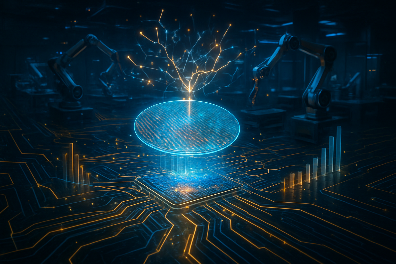
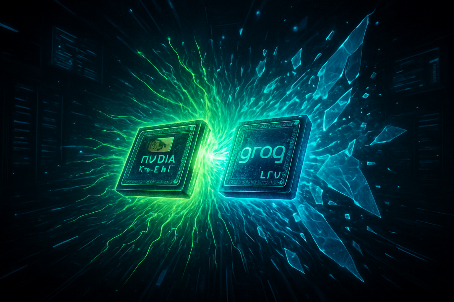
    The landscape of artificial intelligence is undergoing a seismic shift. For years, the industry’s hunger for compute power was satisfied almost exclusively by off-the-shelf hardware, with NVIDIA (NASDAQ: NVDA) reigning supreme as the primary architect of the AI revolution. However, as the demands of large language models (LLMs) grow and the cost of scaling reaches astronomical levels, a new era has dawned: the era of Custom Silicon.

    In a move that underscores the high stakes of this technological rivalry, ByteDance has recently made headlines with a massive $14 billion investment in NVIDIA hardware. Yet, even as they spend billions on third-party chips, the world’s tech titans—Microsoft, Google, and Amazon—are racing to develop their own proprietary processors. This is no longer just a competition for software supremacy; it is a race to own the very "brains" of the digital age.

    The Technical Frontiers of Custom Hardware

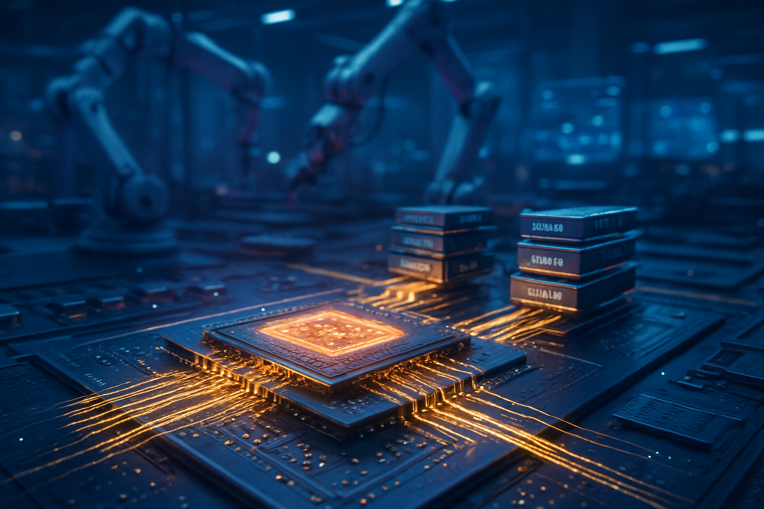
    The shift toward custom silicon is driven by the need for efficiency that general-purpose GPUs can no longer provide at scale. While NVIDIA's H200 and Blackwell architectures are marvels of engineering, they are designed to be versatile. In contrast, in-house chips like Google's Tensor Processing Units (TPUs) are "Application-Specific Integrated Circuits" (ASICs), built from the ground up to do one thing exceptionally well: accelerate the matrix multiplications that power neural networks.

    Google has recently moved into the deployment phase of its TPU v7, codenamed Ironwood. Built on a cutting-edge 3nm process, Ironwood reportedly delivers a staggering 4.6 PFLOPS of dense FP8 compute. With 192GB of high-bandwidth memory (HBM3e), it offers a massive leap in data throughput. This hardware is already being utilized by major partners; Anthropic, for instance, has committed to a landmark deal to use these chips for training its next generation of models, such as Claude 4.5.

    Amazon Web Services (AWS) (NASDAQ: AMZN) is following a similar trajectory with its Trainium 3 chip. Launched recently, Trainium 3 provides a 4x increase in energy efficiency compared to its predecessor. Perhaps most significant is the roadmap for Trainium 4, which is expected to support NVIDIA’s NVLink. This would allow for "mixed clusters" where Amazon’s own chips and NVIDIA’s GPUs can share memory and workloads seamlessly—a level of interoperability that was previously unheard of.

    Microsoft (NASDAQ: MSFT) has taken a slightly different path with Project Fairwater. Rather than just focusing on a standalone chip, Microsoft is re-engineering the entire data center. By integrating its proprietary Azure Boost logic directly into the networking hardware, Microsoft is turning its "AI Superfactories" into holistic systems where the CPU, GPU, and network fabric are co-designed to minimize latency and maximize output for OpenAI's massive workloads.

    Escaping the "NVIDIA Tax"

    The economic incentive for these developments is clear: reducing the "NVIDIA Tax." As the demand for AI grows, the cost of purchasing thousands of H100 or Blackwell GPUs becomes a significant burden on the balance sheets of even the wealthiest companies. By developing their own silicon, the "Big Three" cloud providers can optimize their hardware for their specific software stacks—be it Google’s JAX or Amazon’s Neuron SDK.

    This vertical integration offers several strategic advantages:

    • Cost Reduction: Cutting out the middleman (NVIDIA) and designing chips for specific power envelopes can save billions in the long run.
    • Performance Optimization: Custom silicon can be tuned for specific model architectures, potentially outperforming general-purpose GPUs in specialized tasks.
    • Supply Chain Security: By owning the design, these companies reduce their vulnerability to the supply shortages that have plagued the industry over the past two years.

    However, this doesn't mean NVIDIA's downfall. ByteDance's $14 billion order proves that for many, NVIDIA is still the only game in town for high-end, general-purpose training.

    Geopolitics and the Global Silicon Divide

    The arms race is also being shaped by geopolitical tensions. ByteDance’s massive spend is partly a defensive move to secure as much hardware as possible before potential further export restrictions. Simultaneously, ByteDance is reportedly working with Broadcom (NASDAQ: AVGO) on a 5nm AI ASIC to build its own domestic capabilities.

    This represents a shift toward "Sovereign AI." Governments and multinational corporations are increasingly viewing AI hardware as a national security asset. The move toward custom silicon is as much about independence as it is about performance. We are moving away from a world where everyone uses the same "best" chip, toward a fragmented landscape of specialized hardware tailored to specific regional and industrial needs.

    The Road to 2nm: What Lies Ahead?

    The hardware race is only accelerating. The industry is already looking toward the 2nm manufacturing node, with Apple and NVIDIA competing for limited capacity at TSMC (NYSE: TSM). As we move into 2026 and 2027, the focus will shift from just raw power to interconnectivity and software compatibility.

    The biggest hurdle for custom silicon remains the software layer. NVIDIA’s CUDA platform has a massive headstart with developers. For Microsoft, Google, or Amazon to truly compete, they must make it easy for researchers to port their code to these new architectures. We expect to see a surge in "compiler wars," where companies invest heavily in automated tools that can translate code between different silicon architectures seamlessly.

    A New Era of Innovation

    We are witnessing a fundamental change in how the world's computing infrastructure is built. The era of buying a server and plugging it in is being replaced by a world where the hardware and the AI models are designed in tandem.

    In the coming months, keep an eye on the performance benchmarks of the new TPU v7 and Trainium 3. If these custom chips can consistently outperform or out-price NVIDIA in large-scale deployments, the "Custom Silicon Arms Race" will have moved from a strategic hedge to the new industry standard. The battle for the future of AI will be won not just in the cloud, but in the very transistors that power it.


    This content is intended for informational purposes only and represents analysis of current AI developments.

    TokenRing AI delivers enterprise-grade solutions for multi-agent AI workflow orchestration, AI-powered development tools, and seamless remote collaboration platforms.
    For more information, visit https://www.tokenring.ai/.

  • The $1 Trillion Milestone: AI Demand Drives Semiconductor Industry to Historic 2026 Giga-Cycle

    The $1 Trillion Milestone: AI Demand Drives Semiconductor Industry to Historic 2026 Giga-Cycle

    The global semiconductor industry has reached a historic milestone, officially crossing the $1 trillion annual revenue threshold in 2026—a monumental feat achieved four years earlier than the most optimistic industry projections from just a few years ago. This "Giga-cycle," as analysts have dubbed it, marks the most explosive growth period in the history of silicon, driven by an insatiable global appetite for the hardware required to power the era of Generative AI. While the industry was previously expected to reach this mark by 2030 through steady growth in automotive and 5G, the rapid scaling of trillion-parameter AI models has compressed a decade of technological and financial evolution into a fraction of that time.

    The significance of this milestone cannot be overstated: the semiconductor sector is now the foundational engine of the global economy, rivaling the scale of major energy and financial sectors. Data center capital expenditure (CapEx) from the world’s largest tech giants has surged to approximately $500 billion annually, with a disproportionate share of that spending flowing directly into the coffers of chip designers and foundries. The result is a bifurcated market where high-end Logic and Memory Integrated Circuits (ICs) are seeing year-over-year (YoY) growth rates of 30% to 40%, effectively pulling the rest of the industry across the trillion-dollar finish line years ahead of schedule.

    The Silicon Architecture of 2026: 2nm and HBM4

    The technical foundation of this $1 trillion year is built upon two critical breakthroughs: the transition to the 2-nanometer (2nm) process node and the commercialization of High Bandwidth Memory 4 (HBM4). For the first time, we are seeing the "memory wall"—the bottleneck where data cannot move fast enough between storage and processors—begin to crumble. HBM4 has doubled the interface width to 2,048-bit, providing bandwidth speeds exceeding 2 terabytes per second. More importantly, the industry has shifted to "Logic-in-Memory" architectures, where the base die of the memory stack is manufactured on advanced logic nodes, allowing for basic AI data operations to be performed directly within the memory itself.

    In the logic segment, the move to 2nm process technology by Taiwan Semiconductor Manufacturing Company (NYSE:TSM) and Samsung Electronics (KRX:005930) has enabled a new generation of "Agentic AI" chips. These chips, featuring Gate-All-Around (GAA) transistors and Backside Power Delivery (BSPD), offer a 30% reduction in power consumption compared to the 3nm chips of 2024. This efficiency is critical, as data center power constraints have become the primary limiting factor for AI expansion. The 2026 architectures are designed not just for raw throughput, but for "reasoning-per-watt," a metric that has become the gold standard for the newest AI accelerators like NVIDIA’s Rubin and AMD’s Instinct MI400.

    Industry experts and the AI research community have reacted with a mix of awe and concern. While the leap in compute density allows for the training of models with tens of trillions of parameters, researchers note that the complexity of these new 2nm designs has pushed manufacturing costs to record highs. A single state-of-the-art 2nm wafer now costs nearly $30,000, creating a "barrier to entry" that only the largest corporations and sovereign nations can afford. This has sparked a debate within the community about the "democratization of compute" versus the centralization of power in the hands of a few "trillion-dollar-ready" silicon giants.

    The New Hierarchy: NVIDIA, AMD, and the Foundry Wars

    The financial windfall of the $1 trillion milestone is heavily concentrated among a handful of key players. NVIDIA (NASDAQ:NVDA) remains the dominant force, with its Rubin (R100) architecture serving as the backbone for nearly 80% of global AI data centers. By moving to an annual product release cycle, NVIDIA has effectively outpaced the traditional semiconductor design cadence, forcing its competitors into a permanent state of catch-up. Analysts project NVIDIA’s revenue alone could exceed $215 billion this fiscal year, driven by the massive deployment of its NVL144 rack-scale systems.

    However, the 2026 landscape is more competitive than in previous years. Advanced Micro Devices (NASDAQ:AMD) has successfully captured nearly 20% of the AI accelerator market by being the first to market with 2nm-based Instinct MI400 chips. By positioning itself as the primary alternative to NVIDIA for hyperscalers like Meta and Microsoft, AMD has secured its most profitable year in history. Simultaneously, Intel (NASDAQ:INTC) has reinvented itself through its Foundry services. While its discrete GPUs have seen modest success, its 18A (1.8nm) process node has attracted major external customers, including Amazon and Microsoft, who are now designing their own custom AI silicon to be manufactured in Intel’s domestic fabs.

    The "Memory Supercycle" has also minted new fortunes for SK Hynix (KRX:000660) and Micron Technology (NASDAQ:MU). With HBM4 production being three times more wafer-intensive than standard DDR5 memory, these companies have gained unprecedented pricing power. SK Hynix, in particular, has reported that its entire 2026 HBM4 capacity was sold out before the year even began. This structural shortage of memory has caused a ripple effect, driving up the costs of traditional servers and consumer PCs, as manufacturers divert resources to the high-margin AI segment.

    A Giga-Cycle of Geopolitics and Sovereign AI

    The wider significance of reaching $1 trillion in revenue is tied to the emergence of "Sovereign AI." Nations such as the UAE, Saudi Arabia, and Japan are no longer content with renting cloud space from US-based providers; they are investing billions into domestic "AI Factories." This has created a massive secondary market for high-end silicon that exists independently of the traditional Big Tech demand. This sovereign demand has helped sustain the industry's 30% growth rates even as some Western enterprises began to rationalize their AI experimentation budgets.

    However, this milestone is not without its controversies. The environmental impact of a trillion-dollar semiconductor industry is a growing concern, as the energy required to manufacture and then run these 2nm chips continues to climb. Furthermore, the industry's dependence on specialized lithography and high-purity chemicals has exacerbated geopolitical tensions. Export controls on 2nm-capable equipment and high-end HBM memory remain a central point of friction between major world powers, leading to a fragmented supply chain where "technological sovereignty" is prioritized over global efficiency.

    Comparatively, this achievement dwarfs previous milestones like the mobile boom of the 2010s or the PC revolution of the 1990s. While those cycles were driven by consumer device sales, the current "Giga-cycle" is driven by infrastructure. The semiconductor industry has transitioned from being a supplier of components to the master architect of the digital world. Reaching $1 trillion four years early suggests that the "AI effect" is deeper and more pervasive than even the most bullish analysts predicted in 2022.

    The Road Ahead: Inference at the Edge and Beyond $1 Trillion

    Looking toward the late 2020s, the focus of the semiconductor industry is expected to shift from "Training" to "Inference." As massive models like GPT-6 and its contemporaries complete their initial training phases, the demand will move toward lower-power, highly efficient chips that can run these models on local devices—a trend known as "Edge AI." Experts predict that while data center revenue will remain high, the next $500 billion in growth will come from AI-integrated smartphones, automobiles, and industrial robotics that require real-time reasoning without cloud latency.

    The challenges remaining are primarily physical and economic. As we approach the "1nm" wall, the cost of research and development is ballooning. The industry is already looking toward "3D-stacked logic" and optical interconnects to sustain growth after the 2nm cycle peaks. Many analysts expect a short "digestion period" in 2027 or 2028, where the industry may see a temporary cooling as the initial global build-out of AI infrastructure reaches saturation, but the long-term trajectory remains aggressively upward.

    Summary of a Historic Era

    The semiconductor industry’s $1 trillion milestone in 2026 is a definitive marker of the AI era. Driven by a 30-40% YoY surge in Logic and Memory demand, the industry has fundamentally rewired itself to meet the needs of a world that runs on synthetic intelligence. The key takeaways from this year are clear: the technical dominance of 2nm and HBM4 architectures, the financial concentration among leaders like NVIDIA and TSMC, and the rise of Sovereign AI as a global economic force.

    This development will be remembered as the moment silicon officially became the most valuable commodity on earth. As we move into the second half of 2026, the industry’s focus will remain on managing the structural shortages in memory and navigating the geopolitical complexities of a bifurcated supply chain. For now, the "Giga-cycle" shows no signs of slowing, as the world continues to trade its traditional capital for the processing power of the future.


    This content is intended for informational purposes only and represents analysis of current AI developments.

    TokenRing AI delivers enterprise-grade solutions for multi-agent AI workflow orchestration, AI-powered development tools, and seamless remote collaboration platforms.
    For more information, visit https://www.tokenring.ai/.

  • The Silicon Curtain: Trump’s 25% Semiconductor Tariff and the ‘Build-or-Pay’ Ultimatum Reshaping Global AI

    The Silicon Curtain: Trump’s 25% Semiconductor Tariff and the ‘Build-or-Pay’ Ultimatum Reshaping Global AI

    In a move that has sent shockwaves through the global technology sector and brought the U.S.-China trade war to a fever pitch, President Trump signed a sweeping Section 232 proclamation on January 14, 2026, imposing an immediate 25% tariff on advanced semiconductors. Citing a critical threat to national security due to the United States' reliance on foreign-made logic chips, the administration has framed the move as a necessary "sovereign toll" to force the reshoring of high-tech manufacturing. The proclamation marks a radical shift from targeted export controls to a broad-based fiscal barrier, effectively taxing the very hardware that powers the modern artificial intelligence revolution.

    The geopolitical tension escalated further on January 16, 2026, when Commerce Secretary Howard Lutnick issued a blunt "100% tariff ultimatum" to South Korean memory giants Samsung Electronics (KRX:005930) and SK Hynix (KRX:000660). Speaking at a groundbreaking for a new Micron Technology (NASDAQ:MU) facility, Lutnick declared that foreign memory manufacturers must transition from simple packaging to full-scale wafer fabrication on American soil or face a doubling of their costs at the U.S. border. This "Build-or-Pay" mandate has left international allies and tech conglomerates scrambling to navigate a new era of managed trade where access to the American market is contingent on multi-billion dollar domestic investments.

    Technical Scope and the 'Surgical Strike' on High-End Silicon

    The Section 232 proclamation, titled "Adjusting Imports of Semiconductors," utilizes the Trade Expansion Act of 1962 to implement a two-phase strategy aimed at reclaiming the domestic silicon supply chain. Phase One, which became effective on January 15, 2026, specifically targets high-end logic integrated circuits used in data centers and AI training clusters. The technical parameters for these tariffs are remarkably precise, focusing on chips that exceed a Total Processing Performance (TPP) of 14,000 with a DRAM bandwidth exceeding 4,500 GB/s. This technical "surgical strike" ensures that the 25% levy hits the most powerful hardware currently in production, most notably the H200 series from NVIDIA (NASDAQ:NVDA).

    Unlike previous trade measures that focused on denying China access to technology, this proclamation introduces a "revenue-sharing" model that affects even approved exports. In a paradoxical "whiplash" policy, the administration approved the export of NVIDIA's H200 chips to China on January 13, only to slap a 25% tariff on them the following day. Because these chips, often fabricated by Taiwan Semiconductor Manufacturing Company (NYSE:TSM), must transit through U.S. facilities for mandatory third-party security testing before reaching international buyers, the tariff acts as a mandatory surcharge on every high-end GPU sold globally.

    Industry experts and the AI research community have expressed immediate alarm over the potential for increased R&D costs. While the proclamation includes "carve-outs" for U.S.-based data centers with a power capacity over 100 MW and specific exemptions for domestic startups, the complexity of the Harmonized Tariff Schedule (HTS) codes—specifically 8471.50 and 8473.30—has created a compliance nightmare for hardware integrators. Researchers fear that the increased cost of "compute" will further widen the gap between well-funded tech giants and academic institutions, potentially centralizing AI innovation within a handful of elite, federally-subsidized corporations.

    Corporate Fallout and the Rise of Domestic Champions

    The corporate fallout from the Jan 14 proclamation has been immediate and severe, particularly for NVIDIA and Advanced Micro Devices (NASDAQ:AMD). NVIDIA, which relies on a complex global supply chain that bridges Taiwanese fabrication with U.S. design, now finds itself in the crossfire of a fiscal battle. The 25% tariff on the H200 effectively raises the price of the world’s most sought-after AI chip by tens of thousands of dollars per unit. While NVIDIA's market dominance provides some pricing power, the company faces the risk of a "shadow ban" in China, as Beijing has reportedly instructed domestic firms like Alibaba (NYSE:BABA) and Tencent (OTC:TCEHY) to halt purchases to avoid paying the "Trump Fee" to the U.S. Treasury.

    The big winners in this new landscape appear to be domestic champions with existing U.S. fabrication footprints. Intel (NASDAQ:INTC) has seen its stock buoyed by the prospect of becoming the primary beneficiary of the administration's "Tariffs-for-Investment" model. Under this framework, companies that commit to massive domestic expansions, such as the $500 billion "Taiwan Deal" signed by TSMC, can receive a 15% tariff cap and duty-free import quotas. This creates a tiered competitive environment where those who "build American" enjoy a significant price advantage over foreign competitors who remain tethered to overseas foundries.

    However, for startups and mid-tier AI labs, the disruption to the supply chain could be catastrophic. Existing products that rely on just-in-time delivery of specialized components are seeing lead times extend as customs officials implement the new TPP benchmarks. Market positioning is no longer just about who has the best architecture, but who has the most favorable "tariff offset" status. The strategic advantage has shifted overnight from firms with the most efficient global supply chains to those with the deepest political ties and the largest domestic construction budgets.

    The Geopolitical Schism: A New 'Silicon Curtain'

    This development represents a watershed moment in the broader AI landscape, signaling the end of the "borderless" era of technology development. For decades, the semiconductor industry operated on the principle of comparative advantage, with design in the West and manufacturing in the East. The Section 232 proclamation effectively dismantles this model, replacing it with a "Silicon Curtain" that prioritizes national security and domestic industrial policy over market efficiency. It echoes the steel and aluminum tariffs of 2018 but with far higher stakes, as semiconductors are now viewed as the "oil of the 21st century."

    The geopolitical implications for the U.S.-China trade war are profound. China has already retaliated by implementing a "customs blockade" on H200 shipments in Shenzhen and Hong Kong, signaling that it will not subsidize the U.S. economy through tariff payments. This standoff threatens to bifurcate the global AI ecosystem into two distinct technological blocs: a U.S.-led bloc powered by high-cost, domestically-manufactured silicon, and a China-led bloc forced to accelerate the development of homegrown alternatives like Huawei’s Ascend 910C. The risk of a total "decoupling" has moved from a theoretical possibility to an operational reality.

    Comparisons to previous AI milestones, such as the release of GPT-4 or the initial export bans of 2022, suggest that the 2026 tariffs may be more impactful in the long run. While software breakthroughs define what AI can do, these tariffs define who can afford to do it. The "100% ultimatum" on Samsung and SK Hynix is particularly significant, as it targets the High Bandwidth Memory (HBM) that is essential for all large-scale AI training. By threatening to double the cost of memory, the U.S. is using its market size as a weapon to force a total reconfiguration of the global high-tech map.

    Future Developments: The Race for Reshoring

    Looking ahead, the next several months will be defined by intense negotiations as the administration’s "Phase Two" looms. South Korean officials have already entered "emergency response mode" to seek a deal similar to Taiwan’s, hoping to secure a tariff cap in exchange for accelerated wafer fabrication plants in Texas and Indiana. If Samsung and SK Hynix fail to reach an agreement by mid-2026, the 100% tariff on memory chips could trigger a massive inflationary spike in the cost of all computing hardware, from enterprise servers to high-end consumer electronics.

    The industry also anticipates a wave of "tariff-dodging" innovation. Designers may begin to optimize AI models for lower-performance chips that fall just below the TPP 14,000 threshold, or explore novel architectures that rely less on high-bandwidth memory. However, the technical challenge of maintaining AI progress while operating under fiscal constraints is immense. Near-term, we expect to see an "AI construction boom" across the American Rust Belt and Silicon Prairie, as the combination of CHIPS Act subsidies and Section 232 penalties makes U.S. manufacturing the only viable long-term strategy for global chipmakers.

    Conclusion: Reimagining the Global Supply Chain

    The January 2026 Section 232 proclamation is a definitive assertion of technological sovereignty that will be remembered as a turning point in AI history. By leveraging 25% and 100% tariffs as tools of industrial policy, the Trump administration has fundamentally altered the economics of artificial intelligence. The key takeaways are clear: the era of globalized, low-cost semiconductor supply chains is over, and the future of AI hardware is now inextricably linked to domestic manufacturing capacity and geopolitical loyalty.

    The long-term impact of this "Silicon Curtain" remains to be seen. While it may succeed in reshoring critical manufacturing and securing the U.S. supply chain, it risks stifling global innovation and provoking a permanent technological schism with China. In the coming weeks, the industry will be watching for the outcome of the South Korean negotiations and the planned Trump-Xi Summit in April 2026. For now, the world of AI is in a state of suspended animation, waiting to see if the high cost of the new "sovereign toll" will be the price of security or the cause of a global tech recession.


    This content is intended for informational purposes only and represents analysis of current AI developments.

    TokenRing AI delivers enterprise-grade solutions for multi-agent AI workflow orchestration, AI-powered development tools, and seamless remote collaboration platforms.
    For more information, visit https://www.tokenring.ai/.

  • The Scarcest Resource in AI: HBM4 Memory Sold Out Through 2026 as Hyperscalers Lock in 2048-Bit Future

    The Scarcest Resource in AI: HBM4 Memory Sold Out Through 2026 as Hyperscalers Lock in 2048-Bit Future

    In the relentless pursuit of artificial intelligence supremacy, the focus has shifted from the raw processing power of GPUs to the critical bottleneck of data movement: High Bandwidth Memory (HBM). As of January 21, 2026, the industry has reached a stunning milestone: the world’s three leading memory manufacturers—SK Hynix (KRX: 000660), Samsung Electronics (KRX: 005930), and Micron Technology (NASDAQ: MU)—have officially pre-sold their entire HBM4 production capacity for the 2026 calendar year. This unprecedented "sold out" status highlights a desperate scramble among hyperscalers and chip designers to secure the specialized hardware necessary to run the next generation of generative AI models.

    The immediate significance of this supply crunch cannot be overstated. With NVIDIA (NASDAQ: NVDA) preparing to launch its groundbreaking "Rubin" architecture, the transition to HBM4 represents the most significant architectural overhaul in the history of memory technology. For the AI industry, HBM4 is no longer just a component; it is the scarcest resource on the planet, dictating which tech giants will be able to scale their AI clusters in 2026 and which will be left waiting for 2027 allocations.

    Breaking the Memory Wall: 2048-Bits and 16-Layer Stacks

    The move to HBM4 marks a radical departure from previous generations. The most transformative technical specification is the doubling of the memory interface width from 1024-bit to a massive 2048-bit bus. This "wider pipe" allows HBM4 to achieve aggregate bandwidths exceeding 2 TB/s per stack. By widening the interface, manufacturers can deliver higher data throughput at lower clock speeds, a crucial trade-off that helps manage the extreme power density and heat generation of modern AI data centers.

    Beyond the interface, the industry has successfully transitioned to 16-layer (16-Hi) vertical stacks. At CES 2026, SK Hynix showcased the world’s first working 16-layer HBM4 module, offering capacities between 48GB and 64GB per "cube." To fit 16 layers of DRAM within the standard height limits defined by JEDEC, engineers have pushed the boundaries of material science. SK Hynix continues to refine its Advanced MR-MUF (Mass Reflow Molded Underfill) technology, while Samsung is differentiating itself by being the first to mass-produce HBM4 using a "turnkey" 4nm logic base die produced in its own foundries. This differs from previous generations where the logic die was often a more mature, less efficient node.

    The reaction from the AI research community has been one of cautious optimism tempered by the reality of hardware limits. Experts note that while HBM4 provides the bandwidth necessary to support trillion-parameter models, the complexity of manufacturing these 16-layer stacks is leading to lower initial yields compared to HBM3e. This complexity is exactly why capacity is so tightly constrained; there is simply no margin for error in the manufacturing process when layers are thinned to just 30 micrometers.

    The Hyperscaler Land Grab: Who Wins the HBM War?

    The primary beneficiaries of this memory lock-up are the "Magnificent Seven" and specialized AI chipmakers. NVIDIA remains the dominant force, having reportedly secured the lion’s share of HBM4 capacity for its Rubin R100 GPUs. However, the competitive landscape is shifting as hyperscalers like Alphabet (NASDAQ: GOOGL), Microsoft (NASDAQ: MSFT), Meta Platforms (NASDAQ: META), and Amazon (NASDAQ: AMZN) move to reduce their dependence on external silicon. These companies are using their pre-booked HBM4 allocations for their own custom AI accelerators, such as Google’s TPUv7 and Amazon’s Trainium3, creating a strategic advantage over smaller startups that cannot afford to pre-pay for 2026 capacity years in advance.

    This development creates a significant barrier to entry for second-tier AI labs. While established giants can leverage their balance sheets to "skip the line," smaller companies may find themselves forced to rely on older HBM3e hardware, putting them at a disadvantage in both training speed and inference cost-efficiency. Furthermore, the partnership between SK Hynix and TSMC (NYSE: TSM) has created a formidable "Foundry-Memory Alliance" that complicates Samsung’s efforts to regain its crown. Samsung’s ability to offer a one-stop-shop for logic, memory, and packaging is its main strategic weapon as it attempts to win back market share from SK Hynix.

    Market positioning in 2026 will be defined by "memory-rich" versus "memory-poor" infrastructure. Companies that successfully integrated HBM4 will be able to run larger models on fewer GPUs, drastically reducing the Total Cost of Ownership (TCO) for their AI services. This shift threatens to disrupt existing cloud providers who did not move fast enough to upgrade their hardware stacks, potentially leading to a reshuffling of the cloud market hierarchy.

    The Wider Significance: Moving Past the Compute Bottleneck

    The HBM4 era signifies a fundamental shift in the broader AI landscape. For years, the industry was "compute-limited," meaning the speed of the processor’s logic was the main constraint. Today, we have entered the "bandwidth-limited" era. As Large Language Models (LLMs) grow in size, the time spent moving data from memory to the processor becomes the dominant factor in performance. HBM4 is the industry's collective answer to this "Memory Wall," ensuring that the massive compute capabilities of 2026-era GPUs are not wasted.

    However, this progress comes with significant environmental and economic concerns. The power consumption of HBM4 stacks, while more efficient per gigabyte than HBM3e, still contributes to the spiraling energy demands of AI data centers. The industry is reaching a point where the physical limits of silicon stacking are being tested. The transition to 2048-bit interfaces and 16-layer stacks represents a "Moore’s Law" moment for memory, where the engineering hurdles are becoming as steep as the costs.

    Comparisons to previous AI milestones, such as the initial launch of the H100, suggest that HBM4 will be the defining hardware feature of the 2026-2027 AI cycle. Just as the world realized in 2023 that GPUs were the new oil, the realization in 2026 is that HBM4 is the refined fuel that makes those engines run. Without it, the most advanced AI architectures simply cannot function at scale.

    The Horizon: 20 Layers and the Hybrid Bonding Revolution

    Looking toward 2027 and 2028, the roadmap for HBM4 is already being written. The industry is currently preparing for the transition to 20-layer stacks, which will be required for the "Rubin Ultra" GPUs and the next generation of AI superclusters. This transition will necessitate a move away from traditional "micro-bump" soldering to Hybrid Bonding. Hybrid Bonding eliminates the need for solder balls between DRAM layers, allowing for a 33% increase in stacking density and significantly improved thermal resistance.

    Samsung is currently leading the charge in Hybrid Bonding research, aiming to use its "Hybrid Cube Bonding" (HCB) technology to leapfrog its competitors in the 20-layer race. Meanwhile, SK Hynix and Micron are collaborating with TSMC to perfect wafer-to-wafer bonding processes. The primary challenge remains yield; as the number of layers increases, the probability of a single defect ruining an entire 20-layer stack grows exponentially.

    Experts predict that if Hybrid Bonding is successfully commercialized at scale by late 2026, we could see memory capacities reach 1TB per GPU package by 2028. This would enable "Edge AI" servers to run massive models that currently require entire data center racks, potentially democratizing access to high-tier AI capabilities in the long run.

    Final Assessment: The Foundation of the AI Future

    The pre-sale of 2026 HBM4 capacity marks a turning point in the AI industrial revolution. It confirms that the bottleneck for AI progress has moved deep into the physical architecture of the silicon itself. The collaboration between memory makers like SK Hynix, foundries like TSMC, and designers like NVIDIA has created a new, highly integrated supply chain that is both incredibly powerful and dangerously brittle.

    As we move through 2026, the key indicators to watch will be the production yields of 16-layer stacks and the successful integration of 2048-bit interfaces into the first wave of Rubin-based servers. If manufacturers can hit their production targets, the AI boom will continue unabated. If yields falter, the "Memory War" could turn into a full-scale hardware famine.

    For now, the message to the tech industry is clear: the future of AI is being built on HBM4, and for the next two years, that future has already been bought and paid for.


    This content is intended for informational purposes only and represents analysis of current AI developments.

    TokenRing AI delivers enterprise-grade solutions for multi-agent AI workflow orchestration, AI-powered development tools, and seamless remote collaboration platforms.
    For more information, visit https://www.tokenring.ai/.

  • Silicon Renaissance: Intel 18A Enters High-Volume Production as $5 Billion NVIDIA Alliance Reshapes the AI Landscape

    Silicon Renaissance: Intel 18A Enters High-Volume Production as $5 Billion NVIDIA Alliance Reshapes the AI Landscape

    In a historic shift for the American semiconductor industry, Intel (NASDAQ: INTC) has officially transitioned its 18A (1.8nm-class) process node into high-volume manufacturing (HVM) at its massive Fab 52 facility in Chandler, Arizona. The milestone represents the culmination of CEO Pat Gelsinger’s ambitious "five nodes in four years" strategy, positioning Intel as a formidable challenger to the long-standing dominance of Asian foundries. As of January 21, 2026, the first commercial wafers of "Panther Lake" client processors and "Clearwater Forest" server chips are rolling off the line, signaling that Intel has successfully navigated the most complex transition in its 58-year history.

    The momentum is being further bolstered by a seismic strategic alliance with NVIDIA (NASDAQ: NVDA), which recently finalized a $5 billion investment in the blue chip giant. This partnership, which includes a 4.4% equity stake, marks a pivot for the AI titan as it seeks to diversify its supply chain away from geographical bottlenecks. Together, these developments represent a "Sputnik moment" for domestic chipmaking, merging Intel’s manufacturing prowess with NVIDIA’s undisputed leadership in the generative AI era.

    The 18A Breakthrough and the 1.4nm Frontier

    Intel's 18A node is more than just a reduction in transistor size; it is the debut of two foundational technologies that industry experts believe will define the next decade of computing. The first is RibbonFET, Intel’s implementation of Gate-All-Around (GAA) transistors, which allows for faster switching speeds and reduced leakage. The second, and perhaps more significant for AI performance, is PowerVia. This backside power delivery system separates the power wires from the data wires, significantly reducing resistance and allowing for denser, more efficient chip designs. Reports from Arizona indicate that yields for 18A have already crossed the 60% threshold, a critical mark for commercial profitability that many analysts doubted the company could achieve so quickly.

    While 18A handles the current high-volume needs, the technological "north star" has shifted to the 14A (1.4nm) node. Currently in pilot production at Intel’s D1X "Mod 3" facility in Oregon, the 14A node is the world’s first to utilize High-Numerical Aperture (High-NA) Extreme Ultraviolet (EUV) lithography. These $380 million machines, manufactured by ASML (NASDAQ: ASML), allow for 1.7x smaller features compared to standard EUV tools. By being the first to master High-NA EUV, Intel has gained a projected two-year lead in lithographic resolution over rivals like TSMC (NYSE: TSM) and Samsung, who have opted for a more conservative transition to the new hardware.

    The implementation of these ASML Twinscan EXE:5200B tools at the Ohio One "Silicon Heartland" site is currently the focus of Intel’s long-term infrastructure play. While the Ohio site has faced construction headwinds due to its sheer scale, the facility is being designed from the ground up to be the most advanced lithography hub on the planet. By the time Ohio becomes fully operational later this decade, it is expected to host a fleet of High-NA tools dedicated to the 14A-E (Extended) node, ensuring that the United States remains the center of gravity for sub-2nm fabrication.

    The $5 Billion NVIDIA Alliance: A Strategic Guardrail

    The reported $5 billion alliance between Intel and NVIDIA has sent shockwaves through the tech sector, fundamentally altering the competitive dynamics of the AI chip market. Under the terms of the deal, NVIDIA has secured a significant "private placement" of Intel stock, effectively becoming one of its largest strategic shareholders. While NVIDIA continues to rely on TSMC for its flagship Blackwell and Rubin-class GPUs, the $5 billion commitment serves as a "down payment" on future 18A and 14A capacity. This move provides NVIDIA with a vital domestic secondary source, mitigating the geopolitical risks associated with the Taiwan Strait.

    For Intel Foundry, the NVIDIA alliance acts as the ultimate "seal of approval." Capturing a portion of the world's most valuable chip designer's business validates Intel's transition to a pure-play foundry model. Beyond manufacturing, the two companies are reportedly co-developing "super-stack" AI infrastructure. These systems integrate Intel’s x86 Xeon CPUs with NVIDIA GPUs through proprietary high-speed interconnects, optimized specifically for the 18A process. This deep integration is expected to yield AI training clusters that are 30% more power-efficient than previous generations, a critical factor as global data center energy consumption continues to skyrocket.

    Market analysts suggest that this alliance places immense pressure on other fabless giants, such as Apple (NASDAQ: AAPL) and AMD (NASDAQ: AMD), to reconsider their manufacturing footprints. With NVIDIA effectively "camping out" at Intel's Arizona and Ohio sites, the available capacity for leading-edge nodes is becoming a scarce and highly contested resource. This has allowed Intel to demand more favorable terms and long-term volume commitments from new customers, stabilizing its once-volatile balance sheet.

    Geopolitics and the Domestic Supply Chain

    The success of the 18A rollout is being viewed in Washington D.C. as a triumph for the CHIPS and Science Act. As the largest recipient of federal grants and loans, Intel’s progress is inextricably linked to the U.S. government’s goal of producing 20% of the world's leading-edge chips by 2030. The "Arizona-to-Ohio" corridor represents a strategic redundancy in the global supply chain, ensuring that the critical components of the modern economy—from military AI to consumer smartphones—are no longer dependent on a single geographic point of failure.

    However, the wider significance of this milestone extends beyond national security. The transition to 18A and 14A is happening just as the "Scaling Laws" of AI are being tested by the massive energy requirements of trillion-parameter models. By pioneering PowerVia and High-NA EUV, Intel is providing the hardware efficiency necessary for the next generation of generative AI. Without these advancements, the industry might have hit a "power wall" where the cost of electricity would have outpaced the cognitive gains of larger models.

    Comparing this to previous milestones, the 18A launch is being likened to the transition from vacuum tubes to transistors or the introduction of the first microprocessor. It is not merely an incremental improvement; it is a foundational shift in how matter is manipulated at the atomic scale. The precision required to operate ASML’s High-NA tools is equivalent to "hitting a moving coin on the moon with a laser from Earth," a feat that Intel has now proven it can achieve in a high-volume industrial environment.

    The Road to 10A: What Comes Next

    As 18A matures and 14A moves toward HVM in 2027, Intel is already eyeing the "10A" (1nm) node. Future developments are expected to focus on Complementary FET (CFET) architectures, which stack n-type and p-type transistors on top of each other to save even more space. Experts predict that by 2028, the industry will see the first true 1nm chips, likely coming out of the Ohio One facility as it reaches its full operational stride.

    The immediate challenge for Intel remains the "yield ramp." While 60% is a strong start for 18A, reaching the 80-90% yields typical of mature nodes will require months of iterative tuning. Furthermore, the integration of High-NA EUV into a seamless production flow at the Ohio site remains a logistical hurdle of unprecedented scale. The industry will be watching closely to see if Intel can maintain its aggressive cadence without the "execution stumbles" that plagued the company in the mid-2010s.

    Summary and Final Thoughts

    Intel’s manufacturing comeback, marked by the high-volume production of 18A in Arizona and the pioneering use of High-NA EUV for 14A, represents a turning point in the history of semiconductors. The $5 billion NVIDIA alliance further solidifies this resurgence, providing both the capital and the prestige necessary for Intel to reclaim its title as the world's premier chipmaker.

    This development is a clear signal that the era of U.S. semiconductor manufacturing "outsourcing" is coming to an end. For the tech industry, the implications are profound: more competition in the foundry space, a more resilient global supply chain, and the hardware foundation required to sustain the AI revolution. In the coming months, all eyes will be on the performance of "Panther Lake" in the consumer market and the first 14A test wafers in Oregon, as Intel attempts to turn its technical lead into a permanent market advantage.


    This content is intended for informational purposes only and represents analysis of current AI developments.

    TokenRing AI delivers enterprise-grade solutions for multi-agent AI workflow orchestration, AI-powered development tools, and seamless remote collaboration platforms.
    For more information, visit https://www.tokenring.ai/.

  • The Angstrom Era Arrives: TSMC Enters 2nm Mass Production and Unveils 1.6nm Roadmap

    The Angstrom Era Arrives: TSMC Enters 2nm Mass Production and Unveils 1.6nm Roadmap

    In a definitive moment for the semiconductor industry, Taiwan Semiconductor Manufacturing Company (TSMC: NYSE:TSM) has officially entered the "Angstrom Era." During its Q4 2025 earnings call in mid-January 2026, the foundry giant confirmed that its N2 (2nm) process node reached the milestone of mass production in the final quarter of 2025. This transition marks the most significant architectural shift in a decade, as the industry moves away from the venerable FinFET structure to Nanosheet Gate-All-Around (GAA) technology, a move essential for sustaining the performance gains required by the next generation of generative AI.

    The immediate significance of this rollout cannot be overstated. As the primary forge for the world's most advanced silicon, TSMC’s successful ramp of 2nm ensures that the roadmap for artificial intelligence—and the massive data centers that power it—remains on track. With the N2 node now live, attention has already shifted to the upcoming A16 (1.6nm) node, which introduces the "Super Power Rail," a revolutionary backside power delivery system designed to overcome the physical bottlenecks of traditional chip design.

    Technical Deep-Dive: Nanosheets and the Super Power Rail

    The N2 node represents TSMC’s first departure from the FinFET (Fin Field-Effect Transistor) architecture that has dominated the industry since the 22nm era. In its place, TSMC has implemented Nanosheet GAAFETs, where the gate surrounds the channel on all four sides. This allows for superior electrostatic control, significantly reducing current leakage and enabling a 10–15% speed improvement at the same power level, or a 25–30% power reduction at the same clock speeds compared to the 3nm (N3E) process. Early reports from January 2026 suggest that TSMC has achieved healthy yield rates of 65–75%, a critical lead over competitors like Samsung (KRX:005930) and Intel (NASDAQ:INTC), who have faced yield hurdles during their own GAA transitions.

    Building on the 2nm foundation, TSMC’s A16 (1.6nm) node, slated for volume production in late 2026, introduces the "Super Power Rail" (SPR). While Intel’s "PowerVia" on the 18A node also utilizes backside power delivery, TSMC’s SPR takes a more aggressive approach. By moving the power delivery network to the back of the wafer and connecting it directly to the transistor’s source and drain, TSMC eliminates the need for nano-Through Silicon Vias (nTSVs) that can occupy valuable space. This architectural overhaul frees up the front side of the chip exclusively for signal routing, promising an 8–10% speed boost and up to 20% better power efficiency over the standard N2P process.

    Strategic Impacts: Apple, NVIDIA, and the AI Hyperscalers

    The first beneficiary of the 2nm era is expected to be Apple (NASDAQ:AAPL), which has reportedly secured over 50% of TSMC's initial N2 capacity. The upcoming A20 chip, destined for the iPhone 18 series, will be the flagship for 2nm mobile silicon. However, the most profound impact of the N2 and A16 nodes will be felt in the data center. NVIDIA (NASDAQ:NVDA) has emerged as the lead customer for the A16 node, choosing it for its next-generation "Feynman" GPU architecture. For NVIDIA, the Super Power Rail is not a luxury but a necessity to maintain the energy efficiency levels required for massive AI training clusters.

    Beyond the traditional chipmakers, AI hyperscalers like Microsoft (NASDAQ:MSFT), Alphabet (NASDAQ:GOOGL), and Meta (NASDAQ:META) are utilizing TSMC’s advanced nodes to forge their own destiny. Working through design partners like Broadcom (NASDAQ:AVGO) and Marvell (NASDAQ:MRVL), these tech giants are securing 2nm and A16 capacity for custom AI accelerators. This move allows hyperscalers to bypass off-the-shelf limitations and build silicon specifically tuned for their proprietary large language models (LLMs), further entrenching TSMC as the indispensable gatekeeper of the AI "Giga-cycle."

    The Global Significance of Sub-2nm Scaling

    TSMC's entry into the 2nm era signifies a critical juncture in the global effort to achieve "AI Sovereignty." As AI models grow in complexity, the demand for energy-efficient computing has become a matter of national and corporate security. The shift to A16 and the Super Power Rail is essentially an engineering response to the power crisis facing global data centers. By drastically reducing power consumption per FLOP, these nodes allow for continued AI scaling without necessitating an unsustainable expansion of the electrical grid.

    However, this progress comes at a staggering cost. The industry is currently grappling with "wafer price shock," with A16 wafers estimated to cost between $45,000 and $50,000 each. This high barrier to entry may lead to a bifurcated market where only the largest tech conglomerates can afford the most advanced silicon. Furthermore, the geopolitical concentration of 2nm production in Taiwan remains a focal point for international concern, even as TSMC expands its footprint with advanced fabs in Arizona to mitigate supply chain risks.

    Looking Ahead: The Road to 1.4nm and Beyond

    While N2 is the current champion, the roadmap toward the A14 (1.4nm) node is already being drawn. Industry experts predict that the A14 node, expected around 2027 or 2028, will likely be the point where High-NA (Numerical Aperture) EUV lithography becomes standard for TSMC. This will allow for even tighter feature resolution, though it will require a massive investment in new equipment from ASML (NASDAQ:ASML). We are also seeing early research into 2D materials like carbon nanotubes and molybdenum disulfide (MoS2) to eventually replace silicon as the channel material.

    In the near term, the challenge for the industry lies in packaging. As chiplet designs become the norm for high-performance computing, TSMC’s CoWoS (Chip on Wafer on Substrate) packaging technology will need to evolve in tandem with 2nm and A16 logic. The integration of HBM4 (High Bandwidth Memory) with 2nm logic dies will be the next major technical hurdle to clear in 2026, as the industry seeks to eliminate the "memory wall" that currently limits AI processing speeds.

    A New Benchmark for Computing History

    The commencement of 2nm mass production and the unveiling of the A16 roadmap represent a triumphant defense of Moore’s Law. By successfully navigating the transition to GAAFETs and introducing backside power delivery, TSMC has provided the foundation for the next decade of digital transformation. The 2nm era is not just about smaller transistors; it is about a holistic reimagining of chip architecture to serve the insatiable appetite of artificial intelligence.

    In the coming weeks and months, the industry will be watching for the first benchmark results of N2-based silicon and the progress of TSMC’s Arizona Fab 2, which is slated to bring some of this advanced capacity to U.S. soil. As the competition from Intel’s 18A node heats up, the battle for process leadership has never been more intense—or more vital to the future of global technology.


    This content is intended for informational purposes only and represents analysis of current AI developments.

    TokenRing AI delivers enterprise-grade solutions for multi-agent AI workflow orchestration, AI-powered development tools, and seamless remote collaboration platforms.
    For more information, visit https://www.tokenring.ai/.

  • NVIDIA Seals $20 Billion ‘Acqui-Hire’ of Groq to Power Rubin Platform and Shatter the AI ‘Memory Wall’

    NVIDIA Seals $20 Billion ‘Acqui-Hire’ of Groq to Power Rubin Platform and Shatter the AI ‘Memory Wall’

    In a move that has sent shockwaves through Silicon Valley and global financial markets, NVIDIA (NASDAQ: NVDA) has officially finalized a landmark $20 billion strategic licensing and "acqui-hire" deal with Groq, the pioneer of the Language Processing Unit (LPU). Announced in late December 2025 and moving into full integration phase as of January 2026, the deal represents NVIDIA’s most aggressive maneuver to date to consolidate its lead in the burgeoning "Inference Economy." By absorbing Groq’s core intellectual property and its world-class engineering team—including legendary founder Jonathan Ross—NVIDIA aims to fuse Groq’s ultra-high-speed deterministic compute with its upcoming "Rubin" architecture, scheduled for a late 2026 release.

    The significance of this deal cannot be overstated; it marks a fundamental shift in NVIDIA's architectural philosophy. While NVIDIA has dominated the AI training market for a decade, the industry is rapidly pivoting toward high-volume inference, where speed and latency are the only metrics that matter. By integrating Groq’s specialized LPU technology, NVIDIA is positioning itself to solve the "memory wall"—the physical limitation where data transfer speeds between memory and processors cannot keep up with the demands of massive Large Language Models (LLMs). This acquisition signals the end of the era of general-purpose AI hardware and the beginning of a specialized, inference-first future.

    Breaking the Memory Wall: LPU Tech Meets the Rubin Platform

    The technical centerpiece of this $20 billion deal is the integration of Groq’s SRAM-based (Static Random Access Memory) architecture into NVIDIA’s Rubin platform. Unlike traditional GPUs that rely on High Bandwidth Memory (HBM), which resides off-chip and introduces significant latency penalties, Groq’s LPU utilizes a "software-defined hardware" approach. By placing memory directly on the chip and using a proprietary compiler to pre-schedule every data movement down to the nanosecond, Groq’s tech achieves deterministic performance. In early benchmarks, Groq systems have demonstrated the ability to run models like Llama 3 at speeds exceeding 400 tokens per second—roughly ten times faster than current-generation hardware.

    The Rubin platform, which succeeds the Blackwell architecture, will now feature a hybrid memory hierarchy. While Rubin will still utilize HBM4 for massive model parameters, it is expected to incorporate a "Groq-layer" of high-speed SRAM inference cores. This combination allows the system to overcome the "memory wall" by keeping the most critical, frequently accessed data in the ultra-fast SRAM buffer, while the broader model sits in HBM4. This architectural synergy is designed to support the next generation of "Agentic AI"—autonomous systems that require near-instantaneous reasoning and multi-step planning to function in real-time environments.

    Industry experts have reacted with a mix of awe and concern. Dr. Sarah Chen, lead hardware analyst at SemiAnalysis, noted that "NVIDIA essentially just bought the only viable threat to its inference dominance." The AI research community is particularly excited about the deterministic nature of the Groq-Rubin integration. Unlike current GPUs, which suffer from performance "jitter" due to complex hardware scheduling, the new architecture provides a guaranteed, constant latency. This is a prerequisite for safety-critical AI applications in robotics, autonomous vehicles, and high-frequency financial modeling.

    Strategic Dominance and the 'Acqui-Hire' Model

    This deal is a masterstroke of corporate strategy and regulatory maneuvering. By structuring the agreement as a $20 billion licensing deal combined with a mass talent migration—rather than a traditional acquisition—NVIDIA appears to have circumvented the protracted antitrust scrutiny that famously derailed its attempt to buy ARM in 2022. The deal effectively brings Groq’s 300+ engineers into the NVIDIA fold, with Jonathan Ross, a principal architect of the original Google TPU at Alphabet (NASDAQ: GOOGL), now serving as a Senior Vice President of Inference Architecture at NVIDIA.

    For competitors like Advanced Micro Devices (NASDAQ: AMD) and Intel (NASDAQ: INTC), the NVIDIA-Groq alliance creates a formidable barrier to entry. AMD has made significant strides with its MI300 and MI400 series, but it remains heavily reliant on HBM-based architectures. By pivoting toward the Groq-style SRAM model for inference, NVIDIA is diversifying its technological portfolio in a way that its rivals may struggle to replicate without similar multi-billion-dollar investments. Startups in the AI chip space, such as Cerebras and SambaNova, now face a landscape where the market leader has just absorbed their most potent architectural rival.

    The market implications extend beyond just hardware sales. By controlling the most efficient inference platform, NVIDIA is also solidifying its software moat. The integration of GroqWare—Groq's highly optimized compiler stack—into NVIDIA’s CUDA ecosystem means that developers will be able to deploy ultra-low-latency models without learning an entirely new programming language. This vertical integration ensures that NVIDIA remains the default choice for the world’s largest hyperscalers and cloud service providers, who are desperate to lower the cost-per-token of running AI services.

    A New Era of Real-Time, Agentic AI

    The broader significance of the NVIDIA-Groq deal lies in its potential to unlock "Agentic AI." Until now, AI has largely been a reactive tool—users prompt, and the model responds with a slight delay. However, the future of the industry revolves around agents that can think, plan, and act autonomously. These agents require "Fast Thinking" capabilities that current GPU architectures struggle to provide at scale. By incorporating LPU technology, NVIDIA is providing the "nervous system" required for AI that operates at the speed of human thought, or faster.

    This development also aligns with the growing trend of "Sovereign AI." Many nations are now building their own domestic AI infrastructure to ensure data privacy and national security. Groq had already established a strong foothold in this sector, recently securing a $1.5 billion contract for a data center in Saudi Arabia. By acquiring this expertise, NVIDIA is better positioned to partner with governments around the world, providing turnkey solutions that combine high-performance compute with the specific architectural requirements of sovereign data centers.

    However, the consolidation of such massive power in one company's hands remains a point of concern for the industry. Critics argue that NVIDIA’s "virtual buyout" of Groq further centralizes the AI supply chain, potentially leading to higher prices for developers and limited architectural diversity. Comparison to previous milestones, like the acquisition of Mellanox, suggests that NVIDIA will use this deal to tighten the integration of its networking and compute stacks, making it increasingly difficult for customers to "mix and match" components from different vendors.

    The Road to Rubin and Beyond

    Looking ahead, the next 18 months will be a period of intense integration. The immediate focus is on merging Groq’s compiler technology with NVIDIA’s TensorRT-LLM software. The first hardware fruit of this labor will likely be the R100 "Rubin" GPU. Sources close to the project suggest that NVIDIA is also exploring the possibility of "mini-LPUs"—specialized inference blocks that could be integrated into consumer-grade hardware, such as the rumored RTX 60-series, enabling near-instant local LLM processing on personal workstations.

    Predicting the long-term impact, many analysts believe this deal marks the beginning of the "post-GPU" era for AI. While the term "GPU" will likely persist as a brand, the internal architecture is evolving into a heterogeneous "AI System on a Chip." Challenges remain, particularly in scaling SRAM to the levels required for the trillion-parameter models of 2027 and beyond. Nevertheless, the industry expects that by the time the Rubin platform ships in late 2026, it will set a new world record for inference efficiency, potentially reducing the energy cost of AI queries by an order of magnitude.

    Conclusion: Jensen Huang’s Final Piece of the Puzzle

    The $20 billion NVIDIA-Groq deal is more than just a transaction; it is a declaration of intent. By bringing Jonathan Ross and his LPU technology into the fold, Jensen Huang has successfully addressed the one area where NVIDIA was perceived as potentially vulnerable: ultra-low-latency inference. The "memory wall," which has long been the Achilles' heel of high-performance computing, is finally being dismantled through a combination of SRAM-first design and deterministic software control.

    As we move through 2026, the tech world will be watching closely to see how quickly the Groq team can influence the Rubin roadmap. If successful, this integration will cement NVIDIA’s status not just as a chipmaker, but as the foundational architect of the entire AI era. For now, the "Inference Economy" has a clear leader, and the gap between NVIDIA and the rest of the field has never looked wider.


    This content is intended for informational purposes only and represents analysis of current AI developments.

    TokenRing AI delivers enterprise-grade solutions for multi-agent AI workflow orchestration, AI-powered development tools, and seamless remote collaboration platforms.
    For more information, visit https://www.tokenring.ai/.

  • The Great AI Packaging Squeeze: NVIDIA Secures 50% of TSMC Capacity as SK Hynix Breaks Ground on P&T7

    The Great AI Packaging Squeeze: NVIDIA Secures 50% of TSMC Capacity as SK Hynix Breaks Ground on P&T7

    As of January 20, 2026, the artificial intelligence industry has reached a critical inflection point where the availability of cutting-edge silicon is no longer limited by the ability to print transistors, but by the physical capacity to assemble them. In a move that has sent shockwaves through the global supply chain, NVIDIA (NASDAQ: NVDA) has reportedly secured over 50% of the total advanced packaging capacity from Taiwan Semiconductor Manufacturing Co. (NYSE: TSM), effectively creating a "hard ceiling" for competitors and sovereign AI projects alike. This unprecedented booking of CoWoS (Chip-on-Wafer-on-Substrate) resources highlights a shift in the semiconductor power dynamic, where back-end integration has become the most valuable real estate in technology.

    To combat this bottleneck and secure its own dominance in the memory sector, SK Hynix (KRX: 000660) has officially greenlit a 19 trillion won ($12.9 billion) investment in its P&T7 (Package & Test 7) back-end integration plant. This facility, located in Cheongju, South Korea, is designed to create a direct physical link between high-bandwidth memory (HBM) fabrication and advanced packaging. The crisis of 2026 is defined by this frantic race for "vertical integration," as the industry realizes that designing a world-class AI chip is meaningless if there is no facility equipped to package it.

    The Technical Frontier: CoWoS-L and the HBM4 Integration Challenge

    The current capacity crisis is driven by the extreme physical complexity of NVIDIA’s new Rubin (R100) architecture and the transition to HBM4 memory. Unlike previous generations, the 2026 class of AI accelerators utilizes CoWoS-L (Local Interconnect), a technology that uses silicon bridges to "stitch" together multiple dies into a single massive unit. This allows chips to exceed the traditional "reticle limit," effectively creating processors that are four to nine times the size of a standard semiconductor. These physically massive chips require specialized interposers and precision assembly that only a handful of facilities globally can provide.

    Technical specifications for the 2026 standard have moved toward 12-layer and 16-layer HBM4 stacks, which feature a 2048-bit interface—double the bandwidth of the HBM3E standard used just eighteen months ago. To manage the thermal density and height of these 16-high stacks, the industry is transitioning to "hybrid bonding," a bumpless interconnection method that allows for much tighter vertical integration. Initial reactions from the AI research community suggest that while these advancements offer a 3x leap in training efficiency, the manufacturing yield for such complex "chiplet" designs remains volatile, further tightening the available supply.

    The Competitive Landscape: A Zero-Sum Game for Advanced Silicon

    NVIDIA’s aggressive "anchor tenant" strategy at TSMC has left its rivals, including Advanced Micro Devices (NASDAQ: AMD) and Broadcom (NASDAQ: AVGO), scrambling for the remaining 40-50% of advanced packaging capacity. Reports indicate that NVIDIA has reserved between 800,000 and 850,000 wafers for 2026 to support its Blackwell Ultra and Rubin R100 ramps. This dominance has extended lead times for non-NVIDIA AI accelerators to over nine months, forcing many enterprise customers and cloud providers to double down on NVIDIA’s ecosystem simply because it is the only hardware with a predictable delivery window.

    The strategic advantage for SK Hynix lies in its P&T7 initiative, which aims to bypass external bottlenecks by integrating the entire back-end process. By placing the P&T7 plant adjacent to its M15X DRAM fab, SK Hynix can move HBM4 wafers directly into packaging without the logistical risks of international shipping. This move is a direct challenge to the traditional Outsourced Semiconductor Assembly and Test (OSAT) model, represented by leaders like ASE Technology Holding (NYSE: ASX), which has already raised its 2026 pricing by up to 20% due to the supply-demand imbalance.

    Beyond the Wafer: The Geopolitical and Economic Weight of Advanced Packaging

    The 2026 packaging crisis marks a broader shift in the AI landscape, where "Packaging as the Product" has become the new industry mantra. In previous decades, back-end processing was viewed as a low-margin, commodity phase of production. Today, it is the primary determinant of a company's market cap. The ability to successfully yield a 3D-stacked AI module is now seen as a greater barrier to entry than the design of the chip itself. This has led to a "Sovereign AI" panic, as nations realized that owning a domestic fab is insufficient if the final assembly still relies on a handful of specialized plants in Taiwan or Korea.

    The economic implications are immense. The cost of AI server deployments has surged, driven not by the price of raw silicon, but by the "AI premium" commanded by TSMC and SK Hynix for their packaging expertise. This has created a bifurcated market: tech giants like Google (NASDAQ: GOOGL) and Meta (NASDAQ: META) are accelerating their custom silicon (ASIC) projects to optimize for specific workloads, yet even these internal designs must compete for the same limited CoWoS capacity that NVIDIA has so masterfully cornered.

    The Road to 2027: Glass Substrates and the Next Frontier

    Looking ahead, experts predict that the 2026 crisis will force a radical shift in materials science. The industry is already eyeing 2027 for the mass adoption of glass substrates, which offer better structural integrity and thermal performance than the organic substrates currently causing yield issues. Companies are also exploring "liquid-to-the-chip" cooling as a mandatory requirement, as the power density of 16-layer 3D stacks begins to exceed the limits of traditional air and liquid-cooled data centers.

    The near-term challenge remains the construction timeline for new facilities. While SK Hynix’s P&T7 plant is scheduled to break ground in April 2026, it will not reach full-scale operations until late 2027 or early 2028. This suggests that the "Great Squeeze" will persist for at least another 18 to 24 months, keeping AI hardware prices at record highs and favoring the established players who had the foresight to book capacity years in advance.

    Conclusion: The Year Packaging Defined the AI Era

    The advanced packaging crisis of 2026 has fundamentally rewritten the rules of the semiconductor industry. NVIDIA’s preemptive strike in securing half of the world’s CoWoS capacity has solidified its position at the top of the AI food chain, while SK Hynix’s $12.9 billion bet on the P&T7 plant signals the end of the era where memory and packaging were treated as separate entities.

    The key takeaway for 2026 is that the bottleneck has moved from "how many chips can we design?" to "how many chips can we physically put together?" For investors and tech leaders, the metrics to watch in the coming months are no longer just node migrations (like 3nm to 2nm), but packaging yield rates and the square footage of cleanroom space dedicated to back-end integration. In the history of AI, 2026 will be remembered as the year the industry hit a physical wall—and the year the winners were those who built the biggest doors through it.


    This content is intended for informational purposes only and represents analysis of current AI developments.

    TokenRing AI delivers enterprise-grade solutions for multi-agent AI workflow orchestration, AI-powered development tools, and seamless remote collaboration platforms.
    For more information, visit https://www.tokenring.ai/.

  • NVIDIA’s Spectrum-X Ethernet Photonics: Powering the Million-GPU Era with Light-Speed Efficiency

    NVIDIA’s Spectrum-X Ethernet Photonics: Powering the Million-GPU Era with Light-Speed Efficiency

    As the artificial intelligence industry moves toward the unprecedented scale of million-GPU "superfactories," the physical limits of traditional networking have become the primary bottleneck for progress. Today, January 20, 2026, NVIDIA (NASDAQ:NVDA) has officially moved its Spectrum-X Ethernet Photonics switch system into a critical phase of volume production, signaling a paradigm shift in how data centers operate. By replacing traditional electrical signaling and pluggable optics with integrated Silicon Photonics and Co-Packaged Optics (CPO), NVIDIA is effectively rewiring the brain of the AI data center to handle the massive throughput required by the next generation of Large Language Models (LLMs) and autonomous systems.

    This development is not merely an incremental speed boost; it is a fundamental architectural change. The Spectrum-X Photonics system is designed to solve the "power wall" and "reliability gap" that have plagued massive AI clusters. As AI models grow, the energy required to move data between GPUs has begun to rival the energy used to process it. By integrating light-based communication directly onto the switch silicon, NVIDIA is promising a future where AI superfactories can scale without being strangled by their own power cables or crippled by frequent network failures.

    The Technical Leap: CPO and the End of the "Pluggable" Era

    The heart of the Spectrum-X Photonics announcement lies in the transition to Co-Packaged Optics (CPO). Historically, data centers have relied on pluggable optical transceivers—small modules that convert electrical signals to light at the edge of a switch. However, at speeds of 800G and 1.6T per port, the electrical loss and heat generated by these modules become unsustainable. NVIDIA’s Spectrum SN6800 "super-switch" solves this by housing four ASICs and delivering a staggering 409.6 Tb/s of aggregate bandwidth. By utilizing 200G-per-lane SerDes technology and Micro-Ring Modulators (MRMs), NVIDIA has managed to integrate the optical engines directly onto the switch substrate, reducing signal noise by approximately 5.5x.

    The technical specifications are a testament to the efficiency gains of silicon photonics. The Spectrum-X system reduces power consumption per 1.6T port from a traditional 25 watts down to just 9 watts—a nearly 5x improvement in efficiency. Furthermore, the system is designed for high-radix fabrics, supporting up to 512 ports of 800G in a single "super-switch" configuration. To maintain the thermal stability required for these delicate optical components, the high-end Spectrum-X and Quantum-X variants utilize advanced liquid cooling, ensuring that the photonics engines remain at optimal temperatures even under the heavy, sustained loads typical of AI training.

    Initial reactions from the AI research community and infrastructure architects have been overwhelmingly positive, particularly regarding the system's "link flap-free" uptime. In traditional Ethernet environments, optical-to-electrical transitions are a common point of failure. NVIDIA claims the integrated photonics design achieves 5x longer uptime and 10x greater resiliency compared to standard pluggable solutions. For an AI superfactory where a single network hiccup can stall a multi-million dollar training run for hours, this level of stability is being hailed as the "holy grail" of networking.

    The Photonic Arms Race: Market Impact and Strategic Moats

    The move to silicon photonics has ignited what analysts are calling the "Photonic Arms Race." While NVIDIA is leading with a tightly integrated ecosystem, major competitors like Broadcom (NASDAQ:AVGO), Marvell (NASDAQ:MRVL), and Cisco (NASDAQ:CSCO) are not standing still. Broadcom recently began shipping its Tomahawk 6 (TH6-Davisson) platform, which also boasts 102.4 Tb/s capacity and a highly mature CPO solution. Broadcom’s strategy remains focused on "merchant silicon," providing high-performance chips to a wide range of hardware manufacturers, whereas NVIDIA’s Spectrum-X is optimized to work seamlessly with its own Blackwell and upcoming Rubin GPU platforms.

    This vertical integration provides NVIDIA with a significant strategic advantage. By controlling the GPU, the NIC (Network Interface Card), and now the optical switch, NVIDIA can optimize the entire data path in ways that its competitors cannot. This "full-stack" approach effectively closes the moat around NVIDIA’s ecosystem, making it increasingly difficult for startups or rival chipmakers to offer a compelling alternative that matches the performance and power efficiency of a complete NVIDIA-powered cluster.

    For cloud service providers and tech giants, the decision to adopt Spectrum-X Photonics often comes down to Total Cost of Ownership (TCO). While the initial capital expenditure for liquid-cooled photonic switches is higher than traditional gear, the massive reduction in electricity costs and the increase in cluster uptime provide a clear path to long-term savings. Marvell is attempting to counter this by positioning its Teralynx 10 platform as an "open" alternative, leveraging its 2025 acquisition of Celestial AI to offer a photonic fabric that can connect third-party accelerators, providing a glimmer of hope for a more heterogeneous AI hardware market.

    Beyond the Bandwidth: The Broader AI Landscape

    The shift to light-based communication represents a pivotal moment in the broader AI landscape, comparable to the transition from spinning hard drives to Solid State Drives (SSDs). For years, the industry has focused on increasing the "compute" power of individual chips. However, as we enter the era of "Million-GPU" clusters, the "interconnect" has become the defining factor of AI capability. The Spectrum-X system fits into a broader trend of "physical layer innovation," where the physical properties of light and materials are being exploited to overcome the inherent limitations of electrons in copper.

    This transition also addresses mounting environmental concerns. With data centers projected to consume a significant percentage of global electricity by the end of the decade, the 5x power efficiency improvement offered by silicon photonics is a necessary step toward sustainable AI development. However, the move toward proprietary, high-performance fabrics like Spectrum-X also raises concerns about vendor lock-in and the "Balkanization" of the data center. As the network becomes more specialized for AI, the gap between "commodity" networking and "AI-grade" networking continues to widen, potentially leaving smaller players and academic institutions behind.

    In historical context, the Spectrum-X Photonics launch can be seen as the realization of a decades-long promise. Silicon photonics has been "the technology of the future" for nearly 20 years. Its move into volume production for AI superfactories marks the point where the technology has finally matured from a laboratory curiosity to a mission-critical component of global infrastructure.

    Looking Ahead: The Road to Terabit Networking and Beyond

    As we look toward the remainder of 2026 and into 2027, the roadmap for silicon photonics remains aggressive. While current Spectrum-X systems focus on 800G and 1.6T ports, the industry is already eyeing 3.2T and even 6.4T ports for the 2028 horizon. NVIDIA is expected to continue integrating these optical engines deeper into the compute package, eventually leading to "optical chiplets" where light-based communication happens directly between the GPU dies themselves, bypassing the circuit board entirely.

    One of the primary challenges moving forward will be the "serviceability" of these systems. Because CPO components are integrated directly onto the switch, a single optical failure could traditionally require replacing an entire $100,000 switch. NVIDIA has addressed this in the Spectrum-X design with "detachable" fiber sub-assemblies, but the long-term reliability of these connectors in high-vibration, liquid-cooled environments remains a point of intense interest for data center operators. Experts predict that the next major breakthrough will involve "all-optical switching," where the data never needs to be converted back into electrical form at any point in the network fabric.

    Conclusion: A New Foundation for Intelligence

    NVIDIA’s Spectrum-X Ethernet Photonics system is more than just a faster switch; it is the foundation for the next decade of artificial intelligence. By successfully integrating Silicon Photonics into the heart of the AI superfactory, NVIDIA has addressed the twin crises of power consumption and network reliability that threatened to stall the industry's growth. The 5x reduction in power per port and the significant boost in uptime represent a monumental achievement in data center engineering.

    As we move through 2026, the key metrics to watch will be the speed of adoption among Tier-1 cloud providers and the stability of the photonic engines in real-world, large-scale deployments. While competitors like Broadcom and Marvell will continue to push the boundaries of merchant silicon, NVIDIA’s ability to orchestrate the entire AI stack—from the software layer down to the photons moving between chips—positions them as the undisputed architect of the million-GPU era. The light-speed revolution in AI networking has officially begun.


    This content is intended for informational purposes only and represents analysis of current AI developments.

    TokenRing AI delivers enterprise-grade solutions for multi-agent AI workflow orchestration, AI-powered development tools, and seamless remote collaboration platforms.
    For more information, visit https://www.tokenring.ai/.

  • The Glass Wall: Why Glass Substrates are the Newest Bottleneck in the AI Arms Race

    The Glass Wall: Why Glass Substrates are the Newest Bottleneck in the AI Arms Race

    As of January 20, 2026, the artificial intelligence industry has reached a pivotal juncture where software sophistication is once again being outpaced by the physical limitations of hardware. Following major announcements at CES 2026, it has become clear that the traditional organic substrates used to house the world’s most powerful chips have reached their breaking point. The industry is now racing toward a "Glass Age," as glass substrates emerge as the critical bottleneck determining which companies will dominate the next era of generative AI and sovereign supercomputing.

    The shift is not merely an incremental upgrade but a fundamental re-engineering of how chips are packaged. For decades, the industry relied on organic materials like Ajinomoto Build-up Film (ABF) to connect silicon to circuit boards. However, the massive thermal loads—often exceeding 1,000 watts—generated by modern AI accelerators have caused these organic materials to warp and fail. Glass, with its superior thermal stability and rigidity, has transitioned from a laboratory curiosity to the must-have architecture for the next generation of high-performance computing.

    The Technical Leap: Solving the Scaling Crisis

    The technical shift toward glass-core substrates is driven by three primary factors: thermal expansion, interconnect density, and structural integrity. Organic substrates possess a Coefficient of Thermal Expansion (CTE) that differs significantly from silicon, leading to mechanical stress and "warpage" as chips heat and cool. In contrast, glass can be engineered to match the CTE of silicon almost perfectly. This stability allows for the creation of massive, "reticle-busting" packages exceeding 100mm x 100mm, which are necessary to house the sprawling arrays of chiplets and HBM4 memory stacks that define 2026-era AI hardware.

    Furthermore, glass enables a 10x increase in through-glass via (TGV) density compared to the vias possible in organic layers. This allows for much finer routing—down to sub-2-micron line spacing—enabling faster data transfer between chiplets. Intel (NASDAQ: INTC) has taken an early lead in this space, announcing this month that its Xeon 6+ "Clearwater Forest" processor has officially entered High-Volume Manufacturing (HVM). This marks the first time a commercial CPU has utilized a glass-core substrate, proving that the technology is ready for the rigors of the modern data center.

    The reaction from the research community has been one of cautious optimism tempered by the reality of manufacturing yields. While glass offers unparalleled electrical performance and supports signaling speeds of up to 448 Gbps, its brittle nature makes it difficult to handle in the massive 600mm x 600mm panel formats used in modern factories. Initial yields are reported to be in the 75-85% range, significantly lower than the 95%+ yields common with organic substrates, creating an immediate supply-side bottleneck for the industry's largest players.

    Strategic Realignments: Winners and Losers

    The transition to glass is reshuffling the competitive hierarchy of the semiconductor world. Intel’s decade-long investment in glass research has granted it a significant first-mover advantage, potentially allowing it to regain market share in the high-end server market. Meanwhile, Samsung (KRX: 005930) has leveraged its expertise in display technology to form a "Triple Alliance" between its semiconductor, display, and electro-mechanics divisions. This vertical integration aims to provide a turnkey glass-substrate solution for custom AI ASICs by late 2026, positioning Samsung as a formidable rival to the traditional foundry models.

    TSMC (NYSE: TSM), the current king of AI chip manufacturing, finds itself in a more complex position. While it continues to dominate the market with its silicon-based CoWoS (Chip-on-Wafer-on-Substrate) technology for NVIDIA (NASDAQ: NVDA), TSMC's full-scale glass-based CoPoS (Chip-on-Panel-on-Substrate) platform is not expected to reach mass production until 2027 or 2028. This delay has created a strategic window for competitors and has forced companies like AMD (NASDAQ: AMD) to explore partnerships with SK Hynix (KRX: 000660) and its subsidiary, Absolics, which recently began shipping glass substrate samples from its new $600 million facility in Georgia.

    For AI startups and labs, this bottleneck means that the cost of compute is likely to remain high. As the industry moves away from commodity organic substrates toward specialized glass, the supply chain is tightening. The strategic advantage now lies with those who can secure guaranteed capacity from the few facilities capable of handling glass, such as those owned by Intel or the emerging SK Hynix-Absolics ecosystem. Companies that fail to pivot their chip architectures toward glass may find themselves literally unable to cool their next-generation designs.

    The Warpage Wall and Wider Significance

    The "Warpage Wall" is the hardware equivalent of the "Scaling Law" debate in AI software. Just as researchers question how much further LLMs can scale with existing data, hardware engineers have realized that AI performance cannot scale further with existing materials. The broader significance of glass substrates lies in their ability to act as a platform for Co-Packaged Optics (CPO). Because glass is transparent, it allows for the integration of optical interconnects directly into the chip package, replacing copper wires with light-speed data transmission—a necessity for the trillion-parameter models currently under development.

    However, this transition has exposed a dangerous single-source dependency in the global supply chain. The industry is currently reliant on a handful of specialized materials firms, most notably Nitto Boseki (TYO: 3110), which provides the high-end glass cloth required for these substrates. A projected 10-20% supply gap for high-grade glass materials in 2026 has sent shockwaves through the industry, drawing comparisons to the substrate shortages of 2021. This scarcity is turning glass from a technical choice into a geopolitical and economic lever.

    The move to glass also marks the final departure from the "Moore's Law" era of simple transistor scaling. We have entered the era of "System-on-Package," where the substrate is just as important as the silicon itself. Similar to the introduction of High Bandwidth Memory (HBM) or EUV lithography, the adoption of glass substrates represents a "no-turning-back" milestone. It is the foundation upon which the next decade of AI progress will be built, but it comes with the risk of further concentrating power in the hands of the few companies that can master its complex manufacturing.

    Future Horizons: Beyond the Pilot Phase

    Looking ahead, the next 24 months will be defined by the "yield race." While Intel is currently the only firm in high-volume manufacturing, Samsung and Absolics are expected to ramp up their production lines by the end of 2026. Experts predict that once yields stabilize above 90%, the industry will see a flood of new chip designs that take advantage of the 100mm+ package sizes glass allows. This will likely lead to a new class of "Super-GPUs" that combine dozens of chiplets into a single, massive compute unit.

    One of the most anticipated applications on the horizon is the integration of glass substrates into edge AI devices. While the current focus is on massive data center chips, the superior electrical properties of glass could eventually allow for thinner, more powerful AI-integrated laptops and smartphones. However, the immediate challenge remains the high cost of the specialized manufacturing equipment provided by firms like Applied Materials (NASDAQ: AMAT), which currently face a multi-year backlog for glass-processing tools.

    The Verdict on the Glass Transition

    The transition to glass substrates is more than a technical footnote; it is the physical manifestation of the AI industry's insatiable demand for power and speed. As organic materials fail under the heat of the AI revolution, glass provides the necessary structural and thermal foundation for the future. The current bottleneck is a symptom of a massive industrial pivot—one that favors first-movers like Intel and materials giants like Corning (NYSE: GLW) and Nitto Boseki.

    In summary, the next few months will be critical as more manufacturers transition from pilot samples to high-volume production. The industry must navigate a fragile supply chain and solve significant yield challenges to avoid a prolonged hardware shortage. For now, the "Glass Age" has officially begun, and it will be the defining factor in which AI architectures can survive the intense heat of the coming years. Keep a close eye on yield reports from the new Georgia and Arizona facilities; they will be the best indicators of whether the AI hardware train can keep its current momentum.


    This content is intended for informational purposes only and represents analysis of current AI developments.

    TokenRing AI delivers enterprise-grade solutions for multi-agent AI workflow orchestration, AI-powered development tools, and seamless remote collaboration platforms.
    For more information, visit https://www.tokenring.ai/.