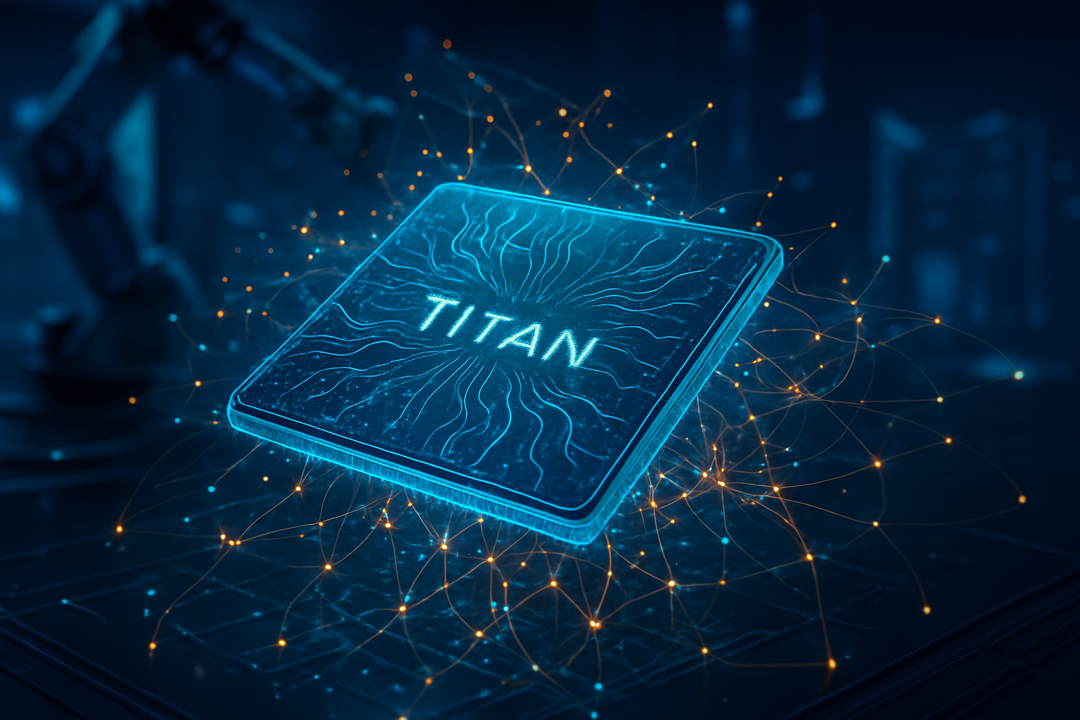
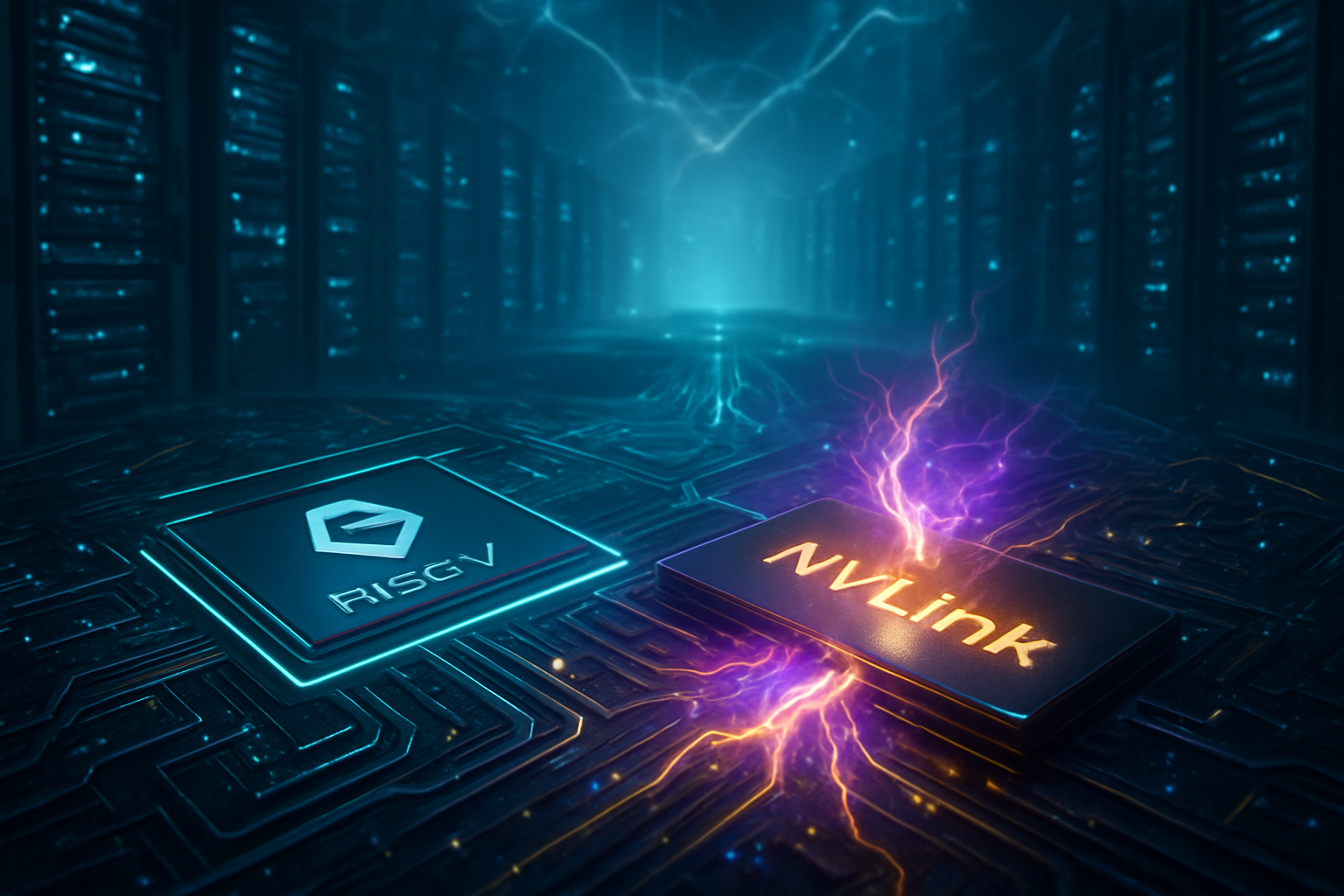
Tag: Nvidia

  • The Rubin Revolution: NVIDIA’s Vera Rubin NVL72 Hits Data Centers, Shattering Efficiency Records

    The Rubin Revolution: NVIDIA’s Vera Rubin NVL72 Hits Data Centers, Shattering Efficiency Records

    The landscape of artificial intelligence has shifted once again as NVIDIA (NASDAQ: NVDA) officially begins the global deployment of its Vera Rubin architecture. As of early 2026, the first production units of the Vera Rubin NVL72 systems have arrived at premier data centers across the United States and Europe, marking the most significant hardware milestone since the release of the Blackwell architecture. This new generation of "AI Factories" arrives at a critical juncture, promising to solve the industry’s twin crises: the insatiable demand for trillion-parameter model training and the skyrocketing energy costs of massive-scale inference.

    This deployment is not merely an incremental update but a fundamental reimagining of data center compute. By integrating the new Vera CPU with the Rubin R100 GPU and HBM4 memory, NVIDIA is delivering on its promise of a 25x reduction in cost and energy consumption for massive language model (LLM) workloads compared to the previous Hopper-generation benchmarks. For the first time, the "agentic AI" era—where AI models reason and act autonomously—has the dedicated, energy-efficient hardware required to scale from experimental labs into the backbone of the global economy.

    A Technical Masterclass: 3nm Silicon and the HBM4 Memory Wall

    The Vera Rubin architecture represents a leap into the 3nm process node, allowing for a 1.6x increase in transistor density over the Blackwell generation. At the heart of the NVL72 rack is the Rubin GPU, which introduces the NVFP4 (4-bit floating point) precision format. This advancement allows the system to process data with significantly fewer bits without sacrificing accuracy, leading to a 5x performance uplift in inference tasks. The NVL72 configuration—a unified, liquid-cooled rack featuring 72 Rubin GPUs and 36 Vera CPUs—operates as a single, massive GPU, capable of processing the world's most complex Mixture-of-Experts (MoE) models with unprecedented fluidity.

    The true "secret sauce" of the Rubin deployment, however, is the transition to HBM4 memory. With a staggering 22 TB/s of bandwidth per GPU, NVIDIA has effectively dismantled the "memory wall" that hampered previous architectures. This massive throughput is paired with the Vera CPU—a custom ARM-based processor featuring 88 "Olympus" cores—which shares a coherent memory pool with the GPU. This co-design ensures that data movement between the CPU and GPU is nearly instantaneous, a requirement for the low-latency reasoning required by next-generation AI agents.

    Initial reactions from the AI research community have been overwhelmingly positive. Dr. Elena Rossi, a lead researcher at the European AI Initiative, noted that "the ability to train a 10-trillion parameter model with one-fourth the number of GPUs required just 18 months ago will democratize high-end AI research." Industry experts highlight the "blind-mate" liquid cooling system and cableless design of the NVL72 as a logistics breakthrough, claiming it reduces the installation and commissioning time of a new AI cluster from weeks to mere days.

    The Hyperscaler Arms Race: Who Benefits from Rubin?

    The deployment of Rubin NVL72 is already reshaping the power dynamics among tech giants. Microsoft (NASDAQ: MSFT) has emerged as the lead partner, integrating Rubin racks into its "Fairwater" AI super-factories. By being the first to market with Rubin-powered Azure instances, Microsoft aims to solidify its lead in the generative AI space, providing the necessary compute for OpenAI’s latest reasoning-heavy models. Similarly, Amazon (NASDAQ: AMZN) and Alphabet (NASDAQ: GOOGL) are racing to update their AWS and Google Cloud footprints, focusing on Rubin’s efficiency to lower the "token tax" for enterprise customers.

    However, the Rubin launch also provides a strategic opening for specialized AI cloud providers like CoreWeave and Lambda. These companies have pivoted their entire business models around NVIDIA's "rack-scale" philosophy, offering early access to Rubin NVL72 to startups that are being priced out of the hyperscale giants. Meanwhile, the competitive landscape is heating up as AMD (NASDAQ: AMD) prepares its Instinct MI400 series. While AMD’s upcoming chip boasts a higher raw memory capacity of 432GB HBM4, NVIDIA’s vertical integration—combining networking, CPU, and GPU into a single software-defined rack—remains a formidable barrier to entry for its rivals.

    For Meta (NASDAQ: META), the arrival of Rubin is a double-edged sword. While Mark Zuckerberg’s company remains one of NVIDIA's largest customers, it is simultaneously investing in its own MTIA chips and the UALink open standard to mitigate long-term reliance on a single vendor. The success of Rubin in early 2026 will determine whether Meta continues its massive NVIDIA spending spree or accelerates its transition to internal silicon for inference workloads.

    The Global Context: Sovereign AI and the Energy Crisis

    Beyond the corporate balance sheets, the Rubin deployment carries heavy geopolitical and environmental significance. The "Sovereign AI" movement has gained massive momentum, with European nations like France and Germany investing billions to build national AI factories using Rubin hardware. By hosting their own NVL72 clusters, these nations aim to ensure that sensitive state data and cultural intelligence remain on domestic soil, reducing their dependence on US-based cloud providers.

    This massive expansion comes at a cost: energy. In 2026, the power consumption of AI data centers has become a top-tier political issue. While the Rubin architecture is significantly more efficient per watt, the sheer volume of GPUs being deployed is straining national grids. This has led to a radical shift in infrastructure, with Microsoft and Amazon increasingly investing in Small Modular Reactors (SMRs) and direct-to-chip liquid cooling to keep their 130kW Rubin racks operational without triggering regional blackouts.

    Comparing this to previous milestones, the Rubin launch feels less like the release of a new chip and more like the rollout of a new utility. In the same way the electrical grid transformed the 20th century, the Rubin NVL72 is being viewed as the foundational infrastructure for a "reasoning economy." Concerns remain, however, regarding the concentration of this power in the hands of a few corporations, and whether the 25x cost reduction will be passed on to consumers or used to pad the margins of the silicon elite.

    Future Horizons: From Generative to Agentic AI

    Looking ahead to the remainder of 2026 and into 2027, the focus will likely shift from the raw training of models to "Physical AI" and autonomous robotics. Experts predict that the Rubin architecture’s efficiency will enable a new class of edge-capable models that can run on-premise in factories and hospitals. The next challenge for NVIDIA will be scaling this liquid-cooled architecture down to smaller footprints without losing the interconnect advantages of the NVLink 6 protocol.

    Furthermore, as the industry moves toward 400 billion and 1 trillion parameter models as the standard, the pressure on memory bandwidth will only increase. We expect to see NVIDIA announce "Rubin Ultra" variations by late 2026, pushing HBM4 capacities even further. The long-term success of this architecture depends on how well the software ecosystem, particularly CUDA 13 and the new "Agentic SDKs," can leverage the massive hardware overhead now available in these data centers.

    Conclusion: The Architecture of the Future

    The deployment of NVIDIA's Vera Rubin NVL72 is a watershed moment for the technology industry. By delivering a 25x improvement in cost and energy efficiency for the most demanding AI tasks, NVIDIA has once again set the pace for the digital age. This hardware doesn't just represent faster compute; it represents the viability of AI as a sustainable, ubiquitous force in modern society.

    As the first racks go live in the US and Europe, the tech world will be watching closely to see if the promised efficiency gains translate into lower costs for developers and more capable AI for consumers. In the coming weeks, keep an eye on the first performance benchmarks from the Microsoft Fairwater facility, as these will likely set the baseline for the "reasoning era" of 2026.


    This content is intended for informational purposes only and represents analysis of current AI developments.

    TokenRing AI delivers enterprise-grade solutions for multi-agent AI workflow orchestration, AI-powered development tools, and seamless remote collaboration platforms.
    For more information, visit https://www.tokenring.ai/.

  • The Half-Trillion Dollar Bet: OpenAI and SoftBank Launch ‘Stargate’ to Build the Future of AGI

    The Half-Trillion Dollar Bet: OpenAI and SoftBank Launch ‘Stargate’ to Build the Future of AGI

    In a move that redefines the scale of industrial investment in the digital age, OpenAI and SoftBank Group (TYO: 9984) have officially broken ground on "Project Stargate," a monumental $500 billion initiative to build a nationwide network of AI supercomputers. This massive consortium, led by SoftBank’s Masayoshi Son and OpenAI’s Sam Altman, represents the largest infrastructure project in American history, aimed at securing the United States' position as the global epicenter of artificial intelligence. By 2029, the partners intend to deploy a unified compute fabric capable of training the first generation of Artificial General Intelligence (AGI).

    The project marks a significant shift in the AI landscape, as SoftBank takes the mantle of primary financial lead for the venture, structured under a new entity called Stargate LLC. While OpenAI remains the operational architect of the systems, the inclusion of global partners like MGX and Oracle (NYSE: ORCL) signals a transition from traditional cloud-based AI scaling to a specialized, gigawatt-scale infrastructure model. The immediate significance is clear: the race for AI dominance is no longer just about algorithms, but about the sheer physical capacity to process data at a planetary scale.

    The Abilene Blueprint: 400,000 Blackwell Chips and Gigawatt Power

    At the heart of Project Stargate is its flagship campus in Abilene, Texas, which has already become the most concentrated hub of compute power on Earth. Spanning over 4 million square feet, the Abilene site is designed to consume a staggering 1.2 gigawatts of power—roughly equivalent to the output of a large nuclear reactor. This facility is being developed in partnership with Crusoe Energy Systems and Blue Owl Capital (NYSE: OWL), with Oracle serving as the primary infrastructure and leasing partner. As of January 2026, the first two buildings are operational, with six more slated for completion by mid-year.

    The technical specifications of the Abilene campus are unprecedented. To power the next generation of "Frontier" models, which researchers expect to feature tens of trillions of parameters, the site is being outfitted with over 400,000 NVIDIA (NASDAQ: NVDA) GB200 Blackwell processors. This single hardware order, valued at approximately $40 billion, represents a departure from previous distributed cloud architectures. Instead of spreading compute across multiple global data centers, Stargate utilizes a "massive compute block" design, utilizing ultra-low latency networking to allow 400,000 GPUs to act as a single, coherent machine. Industry experts note that this architecture is specifically optimized for the "inference-time scaling" and "massive-scale pre-training" required for AGI, moving beyond the limitations of current GPU clusters.

    Shifting Alliances and the New Infrastructure Hegemony

    The emergence of SoftBank as the lead financier of Stargate signals a tactical evolution for OpenAI, which had previously relied almost exclusively on Microsoft (NASDAQ: MSFT) for its infrastructure needs. While Microsoft remains a key technology partner and continues to host OpenAI’s consumer-facing services on Azure, the $500 billion Stargate venture gives OpenAI a dedicated, sovereign infrastructure independent of the traditional "Big Tech" cloud providers. This move provides OpenAI with greater strategic flexibility and positions SoftBank as a central player in the AI hardware revolution, leveraging its ownership of Arm (NASDAQ: ARM) to optimize the underlying silicon architecture of these new data centers.

    This development creates a formidable barrier to entry for other AI labs. Companies like Anthropic or Meta (NASDAQ: META) now face a competitor that possesses a dedicated half-trillion-dollar hardware roadmap. For NVIDIA, the project solidifies its Blackwell architecture as the industry standard, while Oracle’s stock has seen renewed interest as it transforms from a legacy software firm into the physical landlord of the AI era. The competitive advantage is no longer just in the talent of the researchers, but in the ability to secure land, massive amounts of electricity, and the specialized supply chains required to fill 10 gigawatts of data center space.

    A National Imperative: Energy, Security, and the AGI Race

    Beyond the corporate maneuvering, Project Stargate is increasingly viewed through the lens of national security and economic sovereignty. The U.S. government has signaled its support for the project, viewing the 10-gigawatt network as a critical asset in the ongoing technological competition with China. However, the sheer scale of the project has raised immediate concerns regarding the American energy grid. To address the 1.2 GW requirement in Abilene alone, OpenAI and SoftBank have invested $1 billion into SB Energy to develop dedicated solar and battery storage solutions, effectively becoming their own utility provider.

    This initiative mirrors the industrial mobilizations of the 20th century, such as the Manhattan Project or the Interstate Highway System. Critics and environmental advocates have raised questions about the carbon footprint of such massive energy consumption, yet the partners argue that the breakthroughs in material science and fusion energy enabled by these AI systems will eventually offset their own environmental costs. The transition of AI from a "software service" to a "heavy industrial project" is now complete, with Stargate serving as the ultimate proof of concept for the physical requirements of the intelligence age.

    The Roadmap to 2029: 10 Gigawatts and Beyond

    Looking ahead, the Abilene campus is merely the first node in a broader network. Plans are already underway for additional campuses in Milam County, Texas, and Lordstown, Ohio, with new groundbreakings expected in New Mexico and the Midwest later this year. The ultimate goal is to reach 10 gigawatts of total compute capacity by 2029. Experts predict that as these sites come online, we will see the emergence of AI models capable of complex reasoning, autonomous scientific discovery, and perhaps the first verifiable instances of AGI—systems that can perform any intellectual task a human can.

    Near-term challenges remain, particularly in the realm of liquid cooling and specialized power delivery. Managing the heat generated by 400,000 Blackwell chips requires advanced "direct-to-chip" cooling systems that are currently being pioneered at the Abilene site. Furthermore, the geopolitical implications of Middle Eastern investment through MGX will likely continue to face regulatory scrutiny. Despite these hurdles, the momentum behind Stargate suggests that the infrastructure for the next decade of AI development is already being cast in concrete and silicon across the American landscape.

    A New Era for Artificial Intelligence

    The launch of Project Stargate marks the definitive end of the "experimental" phase of AI and the beginning of the "industrial" era. The collaboration between OpenAI and SoftBank, backed by a $500 billion war chest and the world's most advanced hardware, sets a new benchmark for what is possible in technological infrastructure. It is a gamble of historic proportions, betting that the path to AGI is paved with hundreds of thousands of GPUs and gigawatts of electricity.

    As we look toward the remaining years of the decade, the progress of the Abilene campus and its successor sites will be the primary metric for the advancement of artificial intelligence. If successful, Stargate will not only be the world's largest supercomputer network but the foundation for a new form of digital intelligence that could transform every aspect of human society. For now, all eyes are on the Texas plains, where the physical machinery of the future is being built today.


    This content is intended for informational purposes only and represents analysis of current AI developments.

    TokenRing AI delivers enterprise-grade solutions for multi-agent AI workflow orchestration, AI-powered development tools, and seamless remote collaboration platforms.
    For more information, visit https://www.tokenring.ai/.

  • The DeepSeek Effect: How Ultra-Efficient Models Cracked the Code of Semiconductor “Brute Force”

    The DeepSeek Effect: How Ultra-Efficient Models Cracked the Code of Semiconductor “Brute Force”

    The artificial intelligence industry is currently undergoing its most significant structural shift since the "Attention is All You Need" paper, driven by what analysts have dubbed the "DeepSeek Effect." This phenomenon, sparked by the release of DeepSeek-V3 and the reasoning-optimized DeepSeek-R1 in early 2025, has fundamentally shattered the "brute force" scaling laws that defined the first half of the decade. By demonstrating that frontier-level intelligence could be achieved for a fraction of the traditional training cost—most notably training a GPT-4 class model for approximately $6 million—DeepSeek has forced the world's most powerful semiconductor firms to abandon pure TFLOPS (Teraflops) competition in favor of architectural efficiency.

    As of early 2026, the ripple effects of this development have transformed the stock market and data center construction alike. The industry is no longer engaged in a race to build the largest possible GPU clusters; instead, it is pivoting toward a "sparse computation" paradigm. This shift focuses on silicon that can intelligently route data to only the necessary parts of a model, effectively ending the era of dense models where every transistor in a chip fired for every single token processed. The result is a total re-engineering of the AI stack, from the gate level of transistors to the multi-billion-dollar interconnects of global data centers.

    Breaking the Memory Wall: MoE, MLA, and the End of Dense Compute

    At the heart of the DeepSeek Effect are three core technical innovations that have redefined how hardware is utilized: Mixture-of-Experts (MoE), Multi-Head Latent Attention (MLA), and Multi-Token Prediction (MTP). While MoE has existed for years, DeepSeek-V3 scaled it to an unprecedented 671 billion parameters while ensuring that only 37 billion parameters are active for any given token. This "sparse activation" allows a model to possess the "knowledge" of a massive system while only requiring the "compute" of a much smaller one. For chipmakers, this has shifted the priority from raw matrix-multiplication speed to "routing" efficiency—the ability of a chip to quickly decide which "expert" circuit to activate for a specific input.

    The most profound technical breakthrough, however, is Multi-Head Latent Attention (MLA). Previous frontier models suffered from the "KV Cache bottleneck," where the memory required to maintain a conversation’s context grew linearly, eventually choking even the most advanced GPUs. MLA solves this by compressing the Key-Value cache into a low-dimensional "latent" space, reducing memory overhead by up to 93%. This innovation essentially "broke" the memory wall, allowing chips with lower memory capacity to handle massive context windows that were previously the exclusive domain of $40,000 top-tier accelerators.

    Initial reactions from the AI research community were a mix of shock and strategic realignment. Experts at Stanford and MIT noted that DeepSeek’s success proved algorithmic ingenuity could effectively act as a substitute for massive silicon investments. Industry giants who had bet their entire 2025-2030 roadmaps on "brute force" scaling—the idea that more GPUs and more power would always equal more intelligence—were suddenly forced to justify their multi-billion dollar capital expenditures (CAPEX) in a world where a $6 million training run could match their output.

    The Silicon Pivot: NVIDIA, Broadcom, and the Custom ASIC Surge

    The market implications of this shift were felt most acutely on "DeepSeek Monday" in late January 2025, when NVIDIA (NASDAQ: NVDA) saw a historic $600 billion drop in market value as investors questioned the long-term necessity of massive H100 clusters. Since then, NVIDIA has aggressively pivoted its roadmap. In early 2026, the company accelerated the release of its Rubin architecture, which is the first NVIDIA platform specifically designed for sparse MoE models. Unlike the Blackwell series, Rubin features dedicated "MoE Routers" at the hardware level to minimize the latency of expert switching, signaling that NVIDIA is now an "efficiency-first" company.

    While NVIDIA has adapted, the real winners of the DeepSeek Effect have been the custom silicon designers. Broadcom (NASDAQ: AVGO) and Marvell (NASDAQ: MRVL) have seen a surge in orders as AI labs move away from general-purpose GPUs toward Application-Specific Integrated Circuits (ASICs). In a landmark $21 billion deal revealed this month, Anthropic commissioned nearly one million custom "Ironwood" TPU v7p chips from Broadcom. These chips are reportedly optimized for Anthropic’s new Claude architectures, which have fully adopted DeepSeek-style MLA and sparsity to lower inference costs. Similarly, Marvell is integrating "Photonic Fabric" into its 2026 ASICs to handle the high-speed data routing required for decentralized MoE experts.

    Traditional chipmakers like Intel (NASDAQ: INTC) and AMD (NASDAQ: AMD) are also finding new life in this efficiency-focused era. Intel’s "Crescent Island" GPU, launching late this year, bypasses the expensive HBM memory race by using 160GB of high-capacity LPDDR5X. This design is a direct response to the DeepSeek Effect: because MoE models are more "memory-bound" than "compute-bound," having a large, cheaper pool of memory to hold the model's weights is more critical for inference than having the fastest possible compute cores. AMD’s Instinct MI400 has taken a similar path, focusing on massive 432GB HBM4 configurations to house the massive parameter counts of sparse models.

    Geopolitics, Energy, and the New Scaling Law

    The wider significance of the DeepSeek Effect extends beyond technical specifications and into the realms of global energy and geopolitics. By proving that high-tier AI does not require $100 billion "Stargate-class" data centers, DeepSeek has democratized the ability of smaller nations and companies to compete at the frontier. This has sparked a "Sovereign AI" movement, where countries are now investing in smaller, hyper-efficient domestic clusters rather than relying on a few centralized American hyperscalers. The focus has shifted from "How many GPUs can we buy?" to "How much intelligence can we generate per watt?"

    Environmentally, the pivot to sparse computation is the most positive development in AI history. Dense models are notoriously power-hungry because they utilize 100% of their transistors for every operation. DeepSeek-style models, by only activating roughly 5-10% of their parameters per token, offer a theoretical 10x improvement in energy efficiency for inference. As global power grids struggle to keep up with AI demand, the "DeepSeek Effect" has provided a crucial safety valve, allowing intelligence to scale without a linear increase in carbon emissions.

    However, this shift has also raised concerns about the "commoditization of intelligence." If the cost to train and run frontier models continues to plummet, the competitive moat for companies like OpenAI (NASDAQ: MSFT) and Google (NASDAQ: GOOGL) may shift from "owning the best model" to "owning the best data" or "having the best user integration." This has led to a flurry of strategic acquisitions in early 2026, as AI labs rush to secure vertical integrations with hardware providers to ensure they have the most optimized "silicon-to-software" stack.

    The Horizon: Dynamic Sparsity and Edge Reasoning

    Looking forward, the industry is preparing for the release of "DeepSeek-V4" and its competitors, which are expected to introduce "dynamic sparsity." This technology would allow a model to automatically adjust its active parameter count based on the difficulty of the task—using more "experts" for a complex coding problem and fewer for a simple chat interaction. This will require a new generation of hardware with even more flexible gate logic, moving away from the static systolic arrays that have dominated GPU design for the last decade.

    In the near term, we expect to see the "DeepSeek Effect" migrate from the data center to the edge. Specialized Neural Processing Units (NPUs) in smartphones and laptops are being redesigned to handle sparse weights natively. By 2027, experts predict that "Reasoning-as-a-Service" will be handled locally on consumer devices using ultra-distilled MoE models, effectively ending the reliance on cloud APIs for 90% of daily AI tasks. The challenge remains in the software-hardware co-design: as architectures evolve faster than silicon can be manufactured, the industry must develop more flexible, programmable AI chips.

    The ultimate goal, according to many in the field, is the "One Watt Frontier Model"—an AI capable of human-level reasoning that runs on the power budget of a lightbulb. While we are not there yet, the DeepSeek Effect has proven that the path to Artificial General Intelligence (AGI) is not paved with more power and more silicon alone, but with smarter, more elegant ways of utilizing the atoms we already have.

    A New Era for Artificial Intelligence

    The "DeepSeek Effect" will likely be remembered as the moment the AI industry grew up. It marks the transition from a period of speculative "brute force" excess to a mature era of engineering discipline and efficiency. By challenging the dominance of dense architectures, DeepSeek did more than just release a powerful model; it recalibrated the entire global supply chain for AI, forcing the world's largest companies to rethink their multi-year strategies in a matter of months.

    The key takeaway for 2026 is that the value in AI is no longer found in the scale of compute, but in the sophistication of its application. As intelligence becomes cheap and ubiquitous, the focus of the tech industry will shift toward agentic workflows, personalized local AI, and the integration of these systems into the physical world through robotics. In the coming months, watch for more major announcements from Apple (NASDAQ: AAPL) and Meta (NASDAQ: META) regarding their own custom "sparse" silicon as the battle for the most efficient AI ecosystem intensifies.


    This content is intended for informational purposes only and represents analysis of current AI developments.

    TokenRing AI delivers enterprise-grade solutions for multi-agent AI workflow orchestration, AI-powered development tools, and seamless remote collaboration platforms.
    For more information, visit https://www.tokenring.ai/.

  • The Silicon Super-Cycle: Global Semiconductor Market Set to Eclipse $1 Trillion Milestone in 2026

    The Silicon Super-Cycle: Global Semiconductor Market Set to Eclipse $1 Trillion Milestone in 2026

    The global semiconductor industry is standing at the precipice of a historic milestone, with the World Semiconductor Trade Statistics (WSTS) projecting the market to reach $975.5 billion in 2026. This aggressive upward revision, released in late 2025 and validated by early 2026 data, suggests that the industry is flirting with the elusive $1 trillion mark years earlier than analysts had predicted. The surge is being propelled by a relentless "Silicon Super-Cycle" as the world transitions from general-purpose computing to an infrastructure entirely optimized for artificial intelligence.

    As of January 14, 2026, the industry has shifted from a cyclical recovery into a structural boom. The WSTS forecast highlights a staggering 26.3% year-over-year growth rate for the coming year, a figure that has sent shockwaves through global markets. This growth is not evenly distributed but is instead concentrated in the "engines of AI": logic and memory chips. With both segments expected to grow by more than 30%, the semiconductor landscape is being redrawn by the demands of hyperscale data centers and the burgeoning field of physical AI.

    The technical foundation of this $975.5 billion valuation rests on two critical pillars: advanced logic nodes and high-bandwidth memory (HBM). According to WSTS data, the logic segment—which includes the GPUs and specialized accelerators powering AI—is projected to grow by 32.1%, reaching $390.9 billion. This surge is underpinned by the transition to sub-3nm process nodes. NVIDIA (NASDAQ: NVDA) recently announced the full production of its "Rubin" architecture, which delivers a 5x performance leap over the previous Blackwell generation. This advancement is made possible through Taiwan Semiconductor Manufacturing Company (NYSE: TSM), which has successfully scaled its 2nm (N2) process to meet what CEO CC Wei describes as "infinite" demand.

    Equally impressive is the memory sector, which is forecast to be the fastest-growing category at 39.4%. The industry is currently locked in an "HBM Supercycle," where the massive data throughput requirements of AI training and inference have made specialized memory as valuable as the processors themselves. As of mid-January 2026, SK Hynix (KOSPI: 000660) and Samsung Electronics (KOSPI: 005930) are ramping production of HBM4, a technology that offers double the bandwidth of its predecessors. This differs fundamentally from previous cycles where memory was a commodity; today, HBM is a bespoke, high-margin component integrated directly with logic chips using advanced packaging technologies like CoWoS (Chip-on-Wafer-on-Substrate).

    The technical complexity of 2026-era chips has also forced a shift in how systems are built. We are seeing the rise of "rack-scale architecture," where the entire data center rack is treated as a single, massive computer. Advanced Micro Devices (NASDAQ: AMD) recently unveiled its Helios platform, which utilizes this integrated approach to compete for the massive 6-gigawatt (GW) deployment deals being signed by AI labs like OpenAI. Initial reactions from the AI research community suggest that this hardware leap is the primary reason why "reasoning" models and large-scale physical simulations are becoming commercially viable in early 2026.

    The implications for the corporate landscape are profound, as the "Silicon Super-Cycle" creates a widening gap between the leaders and the laggards. NVIDIA continues to dominate the high-end accelerator market, maintaining its position as the world's most valuable company with a market cap exceeding $4.5 trillion. However, the 2026 forecast indicates that the market is diversifying. Intel Corporation (NASDAQ: INTC) has emerged as a major beneficiary of the "Sovereign AI" trend, with its 18A (1.8nm) node now shipping in volume and the U.S. government holding a significant equity stake to ensure domestic supply chain security.

    Foundries and memory providers are seeing unprecedented strategic advantages. TSMC remains the undisputed king of manufacturing, but its capacity is so constrained that it has triggered a "Silicon Shock." This supply-demand imbalance has allowed memory giants like SK Hynix to secure long-term, multi-billion dollar supply agreements that were unheard of five years ago. For startups and smaller AI labs, this environment is challenging; the high cost of entry for state-of-the-art silicon means that the "compute-rich" companies are pulling further ahead in model capability.

    Meanwhile, traditional tech giants are pivotally shifting their strategies to reduce reliance on third-party silicon. Companies like Alphabet Inc. (NASDAQ: GOOGL) and Amazon.com, Inc. (NASDAQ: AMZN) are significantly increasing the deployment of their internal custom ASICs (Application-Specific Integrated Circuits). By 2026, these custom chips are expected to handle over 40% of their internal AI inference workloads, representing a potential long-term disruption to the general-purpose GPU market. This strategic shift allows these giants to optimize their energy consumption and lower the total cost of ownership for their massive cloud divisions.

    Looking at the broader landscape, the path to $1 trillion is about more than just numbers; it represents the "Fourth Industrial Revolution" reaching a point of no return. Analyst Dan Ives of Wedbush Securities has compared the current environment to the early internet boom of 1996, suggesting that for every dollar spent on a chip, there is a $10 multiplier across the tech ecosystem. This multiplier is evident in 2026 as AI moves from digital chatbots to "Physical AI"—the integration of reasoning-based models into robotics, humanoids, and autonomous vehicles.

    However, this rapid growth brings significant concerns regarding sustainability and equity. The energy requirements for the AI infrastructure boom are staggering, leading to a secondary boom in nuclear and renewable energy investments to power the very data centers these chips reside in. Furthermore, the "vampire effect"—where AI chip production cannibalizes capacity for automotive and consumer electronics—has led to price volatility in other sectors, reminding policymakers of the fragile nature of global supply chains.

    Compared to previous milestones, such as the industry hitting $500 billion in 2021, the current surge is characterized by its "structural" rather than "cyclical" nature. In the past, semiconductor growth was driven by consumer cycles in PCs and smartphones. In 2026, the growth is being driven by the fundamental re-architecting of the global economy around AI. The industry is no longer just providing components; it is providing the "cortex" for modern civilization.

    As we look toward the remainder of 2026 and beyond, the next major frontier will be the deployment of AI at the "edge." While the last two years were defined by massive centralized training clusters, the next phase involves putting high-performance AI silicon into billions of devices. Experts predict that "AI Smartphones" and "AI PCs" will trigger a massive replacement cycle by late 2026, as users seek the local processing power required to run sophisticated personal agents without relying on the cloud.

    The challenges ahead are primarily physical and geopolitical. Reaching the sub-1nm frontier will require new materials and even more expensive lithography equipment, potentially slowing the pace of Moore's Law. Geopolitically, the race for "compute sovereignty" will likely intensify, with more nations seeking to establish domestic fab ecosystems to protect their economic interests. By 2027, analysts expect the industry to officially pass the $1.1 trillion mark, driven by the first wave of mass-market humanoid robots.

    The WSTS forecast of $975.5 billion for 2026 is a definitive signal that the semiconductor industry has entered a new era. What was once a cyclical market prone to dramatic swings has matured into the most critical infrastructure on the planet. The fact that the $1 trillion milestone is now a matter of "when" rather than "if" underscores the sheer scale of the AI revolution and its appetite for silicon.

    In the coming weeks and months, investors and industry watchers should keep a close eye on Q1 earnings reports from the "Big Three" foundries and the progress of 2nm production ramps. As the industry knocks on the door of the $1 trillion mark, the focus will shift from simply building the chips to ensuring they can be powered, cooled, and integrated into every facet of human life. 2026 isn't just a year of growth; it is the year the world realized that silicon is the new oil.


    This content is intended for informational purposes only and represents analysis of current AI developments.

    TokenRing AI delivers enterprise-grade solutions for multi-agent AI workflow orchestration, AI-powered development tools, and seamless remote collaboration platforms.
    For more information, visit https://www.tokenring.ai/.

  • The Silicon Revolution: Synopsys and NVIDIA Redefine the Future of Chip Design at CES 2026

    The Silicon Revolution: Synopsys and NVIDIA Redefine the Future of Chip Design at CES 2026

    The semiconductor industry reached a historic turning point at CES 2026 as Synopsys (NASDAQ: SNPS) and NVIDIA (NASDAQ: NVDA) unveiled a series of AI-driven breakthroughs that promise to fundamentally alter how the world's most complex chips are designed and manufactured. Central to the announcement was the maturation of the Synopsys.ai platform, which has transitioned from an experimental toolset into an industrial powerhouse capable of reducing chip design cycles by as much as 12 months. This acceleration represents a seismic shift for the technology sector, effectively compressing three years of traditional research and development into two.

    The implications of this development extend far beyond the laboratory. By leveraging "agentic" AI and high-fidelity virtual prototyping, Synopsys is enabling a "software-first" approach to engineering, particularly in the burgeoning field of software-defined vehicles (SDVs). As chips become more complex at the 2nm and sub-2nm nodes, the traditional bottlenecks of physical prototyping and manual verification are being replaced by AI-native workflows. This evolution is being fueled by a multi-billion dollar commitment from NVIDIA, which is increasingly treating Electronic Design Automation (EDA) not just as a tool, but as a core pillar of its own hardware dominance.

    AgentEngineer and the Rise of Autonomous Chip Design

    The technical centerpiece of Synopsys’ CES showcase was the introduction of AgentEngineer™, an agentic AI framework that marks the next evolution of the Synopsys.ai suite. Unlike previous AI tools that functioned as simple assistants, AgentEngineer utilizes autonomous AI agents capable of reasoning, planning, and executing complex engineering tasks with minimal human intervention. These agents can handle "high-toil" repetitive tasks such as design rule checking, layout optimization, and verification, allowing human engineers to focus on high-level architecture.

    Synopsys also debuted its expanded virtualization portfolio, which integrates technology from its strategic acquisition of Ansys. This integration allows for the creation of "digital twins" of entire electronic stacks long before physical silicon exists. At the heart of this are new Virtualizer Development Kits (VDKs) designed for next-generation automotive architectures, including the Arm Zena compute subsystems and high-performance cores from NXP Semiconductors (NASDAQ: NXPI) and Texas Instruments (NASDAQ: TXN). By providing software teams with virtual System-on-Chip (SoC) models months in advance, Synopsys claims that the time for full system bring-up—once a grueling multi-month process—can now be completed in just a few days.

    This approach differs radically from previous EDA methodologies, which relied heavily on "sequential" development—where software development waited for hardware prototypes. The new "shift-left" paradigm allows for parallel development, slashing the time-to-market for complex systems. Industry experts have noted that the integration of multiphysics simulation (heat, stress, and electromagnetics) directly into the AI design loop represents a breakthrough that was considered a "holy grail" only a few years ago.

    NVIDIA’s $2 Billion Bet on the EDA Ecosystem

    The industry's confidence in this AI-driven future was underscored by NVIDIA’s massive strategic investment. In a move that sent shockwaves through the market, NVIDIA has committed approximately $2 billion to expand its partnership with Synopsys, purchasing millions of shares and deepening technical integration. NVIDIA is no longer just a customer of EDA tools; it is co-architecting the infrastructure. By accelerating the Synopsys EDA stack with its own CUDA libraries and GPU clusters, NVIDIA is optimizing its upcoming GPU architectures—including the newly announced Rubin platform—using the very tools it is helping to build.

    This partnership places significant pressure on other major players in the EDA space, such as Cadence Design Systems (NASDAQ: CDNS) and Siemens (OTC: SIEGY). At CES 2026, NVIDIA also announced an "Industrial AI Operating System" in collaboration with Siemens, which aims to bring generative and agentic workflows to the factory floor and PCB design. The competitive landscape is shifting from who has the best algorithms to who has the most integrated AI-native design stack backed by massive GPU compute power.

    For tech giants and startups alike, this development creates a "winner-takes-most" dynamic. Companies that can afford to integrate these high-end, AI-driven EDA tools will be able to iterate on hardware at a pace that traditional competitors cannot match. Startups in the AI chip space, in particular, may find the 12-month reduction in design cycles to be their only path to survival in a market where hardware becomes obsolete in eighteen months.

    A New Era of "Computers on Wheels" and 2nm Complexity

    The wider significance of these advancements lies in their ability to solve the "complexity wall" of sub-2nm manufacturing. As transistors approach atomic scales, the physics of chip design becomes increasingly unpredictable. AI is the only tool capable of managing the quadrillions of design variables involved in modern lithography. NVIDIA’s cuLitho computational lithography library, integrated with Synopsys and TSMC (NYSE: TSM) workflows, has already reduced lithography simulation times from weeks to overnight, making the mass production of 2nm chips economically viable.

    This shift is most visible in the automotive sector. The "software-defined vehicle" is no longer a buzzword; it is a necessity as cars transition into data centers on wheels. By virtualizing the entire vehicle electronics stack, Synopsys and its partners are reducing prototyping and testing costs by 20% to 60%. This fits into a broader trend where AI is being used to bridge the gap between the digital and physical worlds, a trend seen in other sectors like robotics and aerospace.

    However, the move toward autonomous AI designers also raises concerns. Industry leaders have voiced caution regarding the "black box" nature of AI-generated designs and the potential for systemic errors that human engineers might overlook. Furthermore, the concentration of such powerful design tools in the hands of a few dominant players could lead to a bottleneck in global innovation if access is not democratized.

    The Horizon: From Vera CPUs to Fully Autonomous Fab Integration

    Looking forward, the next two years are expected to bring even deeper integration between AI reasoning and hardware manufacturing. Experts predict that NVIDIA’s Vera CPU—specifically designed for reasoning-heavy agentic AI—will become the primary engine for next-generation EDA workstations. These systems will likely move beyond "assisting" designers to proposing entire architectural configurations based on high-level performance goals, a concept known as "intent-based design."

    The long-term goal is a closed-loop system where AI-driven EDA tools are directly linked to semiconductor fabrication plants (fabs). In this scenario, the design software would receive real-time telemetry from the manufacturing line, automatically adjusting chip layouts to account for minute variations in the production process. While challenges remain—particularly in the standardization of data across different vendors—the progress shown at CES 2026 suggests these hurdles are being cleared faster than anticipated.

    Conclusion: The Acceleration of Human Ingenuity

    The announcements from Synopsys and NVIDIA at CES 2026 mark a definitive end to the era of manual chip design. The ability to slash a year off the development cycle of a modern SoC is a feat of engineering that will ripple through every corner of the global economy, from faster smartphones to safer autonomous vehicles. The integration of agentic AI and virtual prototyping has turned the "shift-left" philosophy from a theoretical goal into a practical reality.

    As we look toward the remainder of 2026, the industry will be watching closely to see how these tools perform in high-volume production environments. The true test will be the first wave of 2nm AI chips designed entirely within these new autonomous frameworks. For now, one thing is certain: the speed of innovation is no longer limited by how fast we can draw circuits, but by how fast we can train the AI to draw them for us.


    This content is intended for informational purposes only and represents analysis of current AI developments.

    TokenRing AI delivers enterprise-grade solutions for multi-agent AI workflow orchestration, AI-powered development tools, and seamless remote collaboration platforms.
    For more information, visit https://www.tokenring.ai/.

  • The Silent Revolution: How Backside Power Delivery is Shattering the AI Performance Wall

    The Silent Revolution: How Backside Power Delivery is Shattering the AI Performance Wall

    The semiconductor industry has officially entered the era of Backside Power Delivery (BSPDN), a fundamental architectural shift that marks the most significant change to transistor design in over a decade. As of January 2026, the long-promised "power wall" that threatened to stall AI progress is being dismantled, not by making transistors smaller, but by fundamentally re-engineering how they are powered. This breakthrough, which involves moving the intricate web of power circuitry from the top of the silicon wafer to its underside, is proving to be the secret weapon for the next generation of AI-ready processors.

    The immediate significance of this development cannot be overstated. For years, chip designers have struggled with a "logistical nightmare" on the silicon surface, where power delivery wires and signal routing wires competed for the same limited space. This congestion led to significant electrical efficiency losses and restricted the density of logic gates. With the debut of Intel’s PowerVia and the upcoming arrival of TSMC’s Super Power Rail, the industry is seeing a leap in performance-per-watt that is essential for sustaining the massive computational demands of generative AI and large-scale inference models.

    A Technical Deep Dive: PowerVia vs. Super Power Rail

    At the heart of this revolution are two competing implementations of BSPDN: PowerVia from Intel Corporation (NASDAQ: INTC) and the Super Power Rail (SPR) from Taiwan Semiconductor Manufacturing Company (NYSE: TSM). Intel has successfully taken the first-mover advantage, with its 18A node and Panther Lake processors hitting high-volume manufacturing in late 2025 and appearing in retail systems this month. Intel’s PowerVia utilizes Nano-Through Silicon Vias (nTSVs) to connect the power network on the back of the wafer to the transistors. This implementation has reduced IR drop—the voltage droop that occurs as electricity travels through a chip—from a standard 7% to less than 1%. By clearing the power lines from the frontside, Intel has achieved a staggering 30% increase in transistor density, allowing for more complex AI engines (NPUs) to be packed into smaller footprints.

    TSMC is taking a more aggressive technical path with its Super Power Rail on the A16 node, scheduled for high-volume production in the second half of 2026. Unlike Intel’s nTSV approach, TSMC’s SPR connects the power network directly to the source and drain of the transistors. While significantly harder to manufacture, this "direct contact" method is expected to offer even higher electrical efficiency. TSMC projects that A16 will deliver a 15-20% power reduction at the same clock frequency compared to its 2nm (N2P) process. This approach is specifically engineered to handle the 1,000-watt power envelopes of future data center GPUs, effectively "shattering the performance wall" by allowing chips to sustain peak boost clocks without the electrical instability that plagued previous architectures.

    Strategic Impacts on AI Giants and Startups

    This shift in manufacturing technology is creating a new competitive landscape for AI companies. Intel’s early lead with PowerVia has allowed it to position its Panther Lake chips as the premier platform for "AI PCs," capable of running 70-billion-parameter LLMs locally on thin-and-light laptops. This poses a direct challenge to competitors who are still reliant on traditional frontside power delivery. For startups and independent AI labs, the increased density means that custom silicon—previously too expensive or complex to design—is becoming more viable, as BSPDN simplifies the physical design rules for high-performance logic.

    Meanwhile, the anticipation for TSMC’s A16 node has already sparked a gold rush among the industry’s heavyweights. Nvidia (NASDAQ: NVDA) is reportedly the anchor customer for A16, intending to use the Super Power Rail to power its 2027 "Feynman" GPU architecture. The ability of A16 to deliver stable, high-amperage power directly to the transistor source is critical for Nvidia’s roadmap, which requires increasingly massive parallel throughput. For cloud giants like Amazon (NASDAQ: AMZN) and Google (NASDAQ: GOOGL), who are developing their own internal AI accelerators (Trainium and TPU), the choice between Intel’s available 18A and TSMC’s upcoming A16 will define their infrastructure efficiency and operational costs for the next three years.

    The Broader Significance: Beyond Moore's Law

    Backside Power Delivery represents more than just a clever engineering trick; it is a paradigm shift that extends the viability of Moore’s Law. As transistors shrunk toward the 2nm and 1.6nm scales, the "wiring bottleneck" became the primary limiting factor in chip performance. By separating the power and data highways into two distinct layers, the industry has effectively doubled the available "real estate" on the chip. This fits into the broader trend of "system-technology co-optimization" (STCO), where the physical structure of the chip is redesigned to meet the specific requirements of AI workloads, which are uniquely sensitive to latency and power fluctuations.

    However, this transition is not without concerns. Moving power to the backside requires complex wafer-thinning and bonding processes that increase the risk of manufacturing defects. Thermal management also becomes more complex; while moving the power grid closer to the cooling solution can help, the extreme power density of these chips creates localized "hot spots" that require advanced liquid cooling or even diamond-based heat spreaders. Compared to previous milestones like the introduction of FinFET transistors, the move to BSPDN is arguably more disruptive because it changes the entire vertical stack of the semiconductor manufacturing process.

    The Horizon: What Comes After 18A and A16?

    Looking ahead, the successful deployment of BSPDN paves the way for the "1nm era" and beyond. In the near term, we expect to see "Backside Signal Routing," where not just power, but also some global clock and data signals are moved to the underside of the wafer to further reduce interference. Experts predict that by 2028, we will see the first true "3D-stacked" logic, where multiple layers of transistors are sandwiched between multiple layers of backside and frontside routing, leading to a ten-fold increase in AI compute density.

    The primary challenge moving forward will be the cost of these advanced nodes. The equipment required for backside processing—specifically advanced wafer bonders and thinning tools—is incredibly expensive, which may lead to a widening gap between the "compute-rich" companies that can afford 1.6nm silicon and those stuck on older, frontside-powered nodes. As AI models continue to grow in size, the ability to manufacture these high-density, high-efficiency chips will become a matter of national economic security, further accelerating the "chip wars" between global superpowers.

    Closing Thoughts on the BSPDN Era

    The transition to Backside Power Delivery marks a historic moment in computing. Intel’s PowerVia has proven that the technology is ready for the mass market today, while TSMC’s Super Power Rail promises to push the boundaries of what is electrically possible by the end of the year. The key takeaway is that the "power wall" is no longer a fixed barrier; it is a challenge that has been solved through brilliant architectural innovation.

    As we move through 2026, the industry will be watching the yields of TSMC’s A16 node and the adoption rates of Intel’s 18A-based Clearwater Forest Xeons. For the AI industry, these technical milestones translate directly into faster training times, more efficient inference, and the ability to run more sophisticated models on everyday devices. The silent revolution on the underside of the silicon wafer is, quite literally, powering the future of intelligence.


    This content is intended for informational purposes only and represents analysis of current AI developments.

    TokenRing AI delivers enterprise-grade solutions for multi-agent AI workflow orchestration, AI-powered development tools, and seamless remote collaboration platforms.
    For more information, visit https://www.tokenring.ai/.

  • Shattering the Warpage Wall: How Glass Substrates are Redefining the Future of AI Chips

    Shattering the Warpage Wall: How Glass Substrates are Redefining the Future of AI Chips

    The semiconductor industry has officially entered the "Glass Age." As of early 2026, the long-standing physical limits of organic packaging materials have finally collided with the insatiable thermal and processing demands of generative AI, sparking a massive industry-wide pivot. Leading the charge are South Korean tech giants Samsung Electro-Mechanics (KRX: 009150) and LG Innotek (KRX: 011070), both of whom have accelerated their roadmaps to replace traditional plastic-based substrates with high-precision glass cores.

    This transition is not merely an incremental upgrade; it is a fundamental architectural shift. Samsung Electro-Mechanics is currently on track to deliver its first commercial prototypes by the end of 2026, while LG Innotek has set a firm sights on 2028 for full-scale mass production. For the AI industry, which is currently struggling to scale hardware beyond the 1,000-watt threshold, glass substrates represent the "holy grail" of packaging—offering the structural integrity and electrical performance required to power the next generation of "super-chips."

    Breaking the "Warpage Wall" with Glass Precision

    At the heart of this shift is a phenomenon known as the "warpage wall." For decades, the industry has relied on Ajinomoto Build-up Film (ABF), an organic, plastic-like material, to connect silicon chips to circuit boards. However, as AI accelerators from companies like NVIDIA (NASDAQ: NVDA) and AMD (NASDAQ: AMD) grow larger and hotter, these organic materials have reached their breaking point. Because organic substrates have a significantly higher Coefficient of Thermal Expansion (CTE) than the silicon they support, they physically warp and bend under extreme heat. This deformation leads to "cracked micro-bumps"—microscopic failures in the electrical connections that render the entire chip useless.

    Glass substrates solve this by matching the CTE of silicon almost perfectly. By providing a substrate that remains ultra-flat even at temperatures exceeding those found in high-density data centers, manufacturers can build packages larger than 100mm x 100mm—a feat previously impossible with organic materials. Furthermore, glass allows for a "40% better signal integrity" profile, primarily through a dramatic reduction in signal loss. This efficiency enables data to move across the package with up to 50% lower power consumption, a critical metric for hyperscalers like Amazon (NASDAQ: AMZN) and Microsoft (NASDAQ: MSFT) who are battling rising energy costs in their AI infrastructures.

    The technical superiority of glass also extends to interconnect density. Unlike organic substrates that require mechanical drilling, glass uses laser-etched Through-Glass Vias (TGVs). This allows for a 10-fold increase in the number of vertical connections, enabling designers to pack dozens of High Bandwidth Memory (HBM) stacks directly around a GPU. Industry experts have described this as a "once-in-a-generation" leap that effectively bypasses the physical scaling limits that once threatened the post-Moore’s Law era.

    A Battle of Giants: Samsung vs. Intel vs. LG Innotek

    The race for glass supremacy has created a new competitive frontier among the world’s largest semiconductor players. Samsung Electro-Mechanics has utilized a "Triple Alliance" strategy, drawing on the glass-processing expertise of Samsung Display and the chip-making prowess of Samsung Electronics to fast-track its Sejong-based pilot line. Samsung CEO Chang Duck-hyun recently noted that 2026 will be the "defining year" for the commercialization of these "dream substrates," positioning the company to be a primary supplier for the next wave of AI hardware.

    However, they are not alone. Intel (NASDAQ: INTC), an early pioneer in the space, has already moved into high-volume manufacturing (HVM) at its Arizona facility, aiming to integrate glass cores into its 18A and 14A process nodes. Meanwhile, LG Innotek is playing a more calculated long-game. While their mass production target is 2028, LG Innotek CEO Moon Hyuk-soo has emphasized that the company is focusing on solving the industry's most nagging problem: glass brittleness. "Whoever solves the issue of glass cracking first will lead the market," Moon stated during a recent industry summit, highlighting LG’s focus on durability and yield over immediate speed-to-market.

    This competition is also drawing in traditional foundry leaders. TSMC (NYSE: TSM) has recently pivoted toward Fan-Out Panel-Level Packaging (FO-PLP) on glass to support future architectures like NVIDIA’s "Rubin" R100 GPUs. As these companies vie for dominance, the strategic advantage lies in who can most efficiently transition from 300mm circular wafers to massive 600mm x 600mm rectangular glass panels—a shift known as the "Rectangular Revolution" that promises to slash manufacturing costs while increasing usable area by over 80%.

    The Wider Significance: Enabling the 1,000-Watt AI Era

    The move to glass substrates is a direct response to the "energy wall" facing modern AI. As models grow more complex, the hardware required to train them has become increasingly power-hungry. Traditional packaging methods have become a bottleneck, both in terms of heat dissipation and the energy required just to move data between the processor and memory. By improving signal integrity and thermal management, glass substrates are essentially "widening the pipe" for AI computation, allowing for more performant chips that are simultaneously more energy-efficient.

    This shift also marks a broader trend toward "System-in-Package" (SiP) innovation. In the past, performance gains came primarily from shrinking transistors on the silicon itself. Today, as that process becomes exponentially more expensive and difficult, the industry is looking to the package—the "house" the chip lives in—to drive the next decade of performance. Glass is the foundation of this new house, enabling a modular "chiplet" approach where different types of processors and memory can be tiled together with near-zero latency.

    However, the transition is not without its risks. The primary concern remains the inherent fragility of glass. While it is thermally stable, it is susceptible to "micro-cracks" during the manufacturing process, which can lead to catastrophic yield losses. The industry's ability to develop automated handling equipment that can manage these ultra-thin glass panels at scale will determine how quickly the technology trickles down from high-end AI servers to consumer electronics.

    Future Developments and the Road to 2030

    Looking ahead, the roadmap for glass substrates extends far beyond 2026. While the immediate focus is on 1,000-watt AI accelerators for data centers, analysts expect the technology to migrate into high-end laptops and mobile devices by the end of the decade. By 2028, when LG Innotek enters the fray with its mass-production lines, we may see the first "all-glass" mobile processors, which could offer significant battery life improvements due to the reduced power required for internal data movement.

    The next two years will be characterized by rigorous testing and "qualification cycles." Hyperscalers are currently evaluating prototypes from Samsung and Absolics—a subsidiary of SKC (KRX: 011790)—to ensure these new substrates can survive the 24/7 high-heat environments of modern AI clusters. If these tests are successful, 2027 could see a massive "lift and shift" where glass becomes the standard for all high-performance computing (HPC) applications.

    Experts also predict that the rise of glass substrates will trigger a wave of mergers and acquisitions in the materials science sector. Traditional chemical suppliers will need to adapt to a world where glass-handling equipment and laser-via technologies are as essential as the silicon itself. The "cracking problem" remains the final technical hurdle, but with the combined R&D budgets of Samsung, LG, and Intel focused on the issue, a solution is widely expected before the 2028 production window.

    A New Foundation for Artificial Intelligence

    The shift toward glass substrates represents one of the most significant changes in semiconductor packaging in over twenty years. By solving the "warpage wall" and providing a 40% boost to signal integrity, glass is providing the physical foundation upon which the next decade of AI breakthroughs will be built. Samsung Electro-Mechanics’ aggressive 2026 timeline and LG Innotek’s specialized 2028 roadmap show that the industry's heaviest hitters are fully committed to this "Glass Age."

    As we move toward the end of 2026, the industry will be watching Samsung's pilot line in Sejong with intense scrutiny. Its success—or failure—to achieve high yields will serve as the first real-world test of whether glass can truly replace organic materials on a global scale. For now, the message from the semiconductor world is clear: the future of AI is no longer just about the silicon; it is about the glass that holds it all together.


    This content is intended for informational purposes only and represents analysis of current AI developments.

    TokenRing AI delivers enterprise-grade solutions for multi-agent AI workflow orchestration, AI-powered development tools, and seamless remote collaboration platforms.
    For more information, visit https://www.tokenring.ai/.

  • The 2,048-Bit Breakthrough: Inside the HBM4 Memory War at CES 2026

    The 2,048-Bit Breakthrough: Inside the HBM4 Memory War at CES 2026

    The Consumer Electronics Show (CES) 2026 has officially transitioned from a showcase of consumer gadgets to the primary battlefield for the most critical component in the artificial intelligence era: High Bandwidth Memory (HBM). What industry analysts are calling the "HBM4 Memory War" reached a fever pitch this week in Las Vegas, as the world’s leading semiconductor giants unveiled their most advanced memory architectures to date. The stakes have never been higher, as these chips represent the fundamental infrastructure required to power the next generation of generative AI models and autonomous systems.

    At the center of the storm is the formal introduction of the HBM4 standard, a revolutionary leap in memory technology designed to shatter the "memory wall" that has plagued AI scaling. As NVIDIA (NASDAQ: NVDA) prepares to launch its highly anticipated "Rubin" GPU architecture, the race to supply the necessary bandwidth has seen SK Hynix (KRX: 000660), Samsung Electronics (KRX: 005930), and Micron Technology (NASDAQ: MU) deploy their most aggressive technological roadmaps in history. The victor of this conflict will likely dictate the pace of AI development for the remainder of the decade.

    Engineering the 16-Layer Titan

    SK Hynix stole the spotlight at CES 2026 by demonstrating the world’s first 16-layer (16-Hi) HBM4 module, a massive 48GB stack that represents a nearly 50% increase in capacity over current HBM3E solutions. The technical centerpiece of this announcement is the implementation of a 2,048-bit interface—double the 1,024-bit width that has been the industry standard for a decade. By "widening the pipe" rather than simply increasing clock speeds, SK Hynix has achieved an unprecedented data throughput of 1.6 TB/s per stack, all while significantly reducing the power consumption and heat generation that have become major obstacles in modern data centers.

    To achieve this 16-layer density, SK Hynix utilized its proprietary Advanced Mass Reflow Molded Underfill (MR-MUF) technology, thinning individual DRAM wafers to a staggering 30 micrometers—roughly the thickness of a human hair. This allows the company to stack 16 layers of high-density DRAM within the same physical height as previous 12-layer designs. Furthermore, the company highlighted a strategic alliance with TSMC (NYSE: TSM), using a specialized 12nm logic base die at the bottom of the stack. This collaboration allows for deeper integration between the memory and the processor, effectively turning the memory stack into a semi-intelligent co-processor that can handle basic data pre-processing tasks.

    Initial reactions from the semiconductor research community have been overwhelmingly positive, though some experts caution about the manufacturing complexity. Dr. Elena Vos, Lead Architect at Silicon Analytics, noted that while the 2,048-bit interface is a "masterstroke of efficiency," the move toward hybrid bonding and extreme wafer thinning raises significant yield concerns. However, SK Hynix’s demonstration showed functional silicon running at 10 GT/s, suggesting that the company is much closer to mass production than its rivals might have hoped.

    A Three-Way Clash for AI Dominance

    While SK Hynix focused on density and interface width, Samsung Electronics counter-attacked with a focus on manufacturing efficiency and power. Samsung unveiled its HBM4 lineup based on its 1c nanometer process—the sixth generation of its 10nm-class DRAM. Samsung claims that this advanced node provides a 40% improvement in energy efficiency compared to competing 1b-based modules. In an era where NVIDIA's top-tier GPUs are pushing past 1,000 watts, Samsung is positioning its HBM4 as the only viable solution for sustainable, large-scale AI deployments. Samsung also signaled a massive production ramp-up at its Pyeongtaek facility, aiming to reach 250,000 wafers per month by the end of the year to meet the insatiable demand from hyperscalers.

    Micron Technology, meanwhile, is leveraging its status as a highly efficient "third player" to disrupt the market. Micron used CES 2026 to announce that its entire HBM4 production capacity for the year has already been sold out through advance contracts. With a $20 billion capital expenditure plan and new manufacturing sites in Taiwan and Japan, Micron is banking on a "supply-first" strategy. While their early HBM4 modules focus on 12-layer stacks, they have promised a rapid transition to "HBM4E" by 2027, featuring 64GB capacities. This aggressive roadmap is clearly aimed at winning a larger share of the bill of materials for NVIDIA’s upcoming Rubin platform.

    The primary beneficiary of this memory war is undoubtedly NVIDIA. The upcoming Rubin GPU is expected to utilize eight stacks of HBM4, providing a total of 384GB of high-speed memory and an aggregate bandwidth of 22 TB/s. This is nearly triple the bandwidth of the current Blackwell architecture, a requirement driven by the move toward "Reasoning Models" and Mixture-of-Experts (MoE) architectures that require massive amounts of data to be swapped in and out of the GPU memory at lightning speed.

    Shattering the Memory Wall: The Strategic Stakes

    The significance of the HBM4 transition extends far beyond simple speed increases; it represents a fundamental shift in how computers are built. For decades, the "Von Neumann bottleneck"—the delay caused by the distance and speed limits between a processor and its memory—has limited computational performance. HBM4, with its 2,048-bit interface and logic-die integration, essentially fuses the memory and the processor together. This is the first time in history where memory is not just a storage bin, but a customized, active participant in the AI computation process.

    This development is also a critical geopolitical and economic milestone. As nations race toward "Sovereign AI," the ability to secure a stable supply of high-performance memory has become a matter of national security. The massive capital requirements—running into the tens of billions of dollars for each company—ensure that the HBM market remains a highly exclusive club. This consolidation of power among SK Hynix, Samsung, and Micron creates a strategic choke point in the global AI supply chain, making these companies as influential as the foundries that print the AI chips themselves.

    However, the "war" also brings concerns regarding the environmental footprint of AI. While HBM4 is more efficient per gigabyte of data transferred, the sheer scale of the units being deployed will lead to a net increase in data center power consumption. The shift toward 1,000-watt GPUs and multi-kilowatt server racks is forcing a total rethink of liquid cooling and power delivery infrastructure, creating a secondary market boom for cooling specialists and electrical equipment manufacturers.

    The Horizon: Custom Logic and the Road to HBM5

    Looking ahead, the next phase of the memory war will likely involve "Custom HBM." At CES 2026, both SK Hynix and Samsung hinted at future products where customers like Google or Amazon (NASDAQ: AMZN) could provide their own proprietary logic to be integrated directly into the HBM4 base die. This would allow for even more specialized AI acceleration, potentially moving functions like encryption, compression, and data search directly into the memory stack itself.

    In the near term, the industry will be watching the "yield race" closely. Demonstrating a 16-layer stack at a trade show is one thing; consistently manufacturing them at the millions-per-month scale required by NVIDIA is another. Experts predict that the first half of 2026 will be defined by rigorous qualification tests, with the first Rubin-powered servers hitting the market late in the fourth quarter. Meanwhile, whisperings of HBM5 are already beginning, with early proposals suggesting another doubling of the interface or the move to 3D-integrated memory-on-logic architectures.

    A Decisive Moment for the AI Hardware Stack

    The CES 2026 HBM4 announcements represent a watershed moment in semiconductor history. We are witnessing the end of the "general purpose" memory era and the dawn of the "application-specific" memory age. SK Hynix’s 16-Hi breakthrough and Samsung’s 1c process efficiency are not just technical achievements; they are the enabling technologies that will determine whether AI can continue its exponential growth or if it will be throttled by hardware limitations.

    As we move forward into 2026, the key indicators of success will be yield rates and the ability of these manufacturers to manage the thermal complexities of 3D stacking. The "Memory War" is far from over, but the opening salvos at CES have made one thing clear: the future of artificial intelligence is no longer just about the speed of the processor—it is about the width and depth of the memory that feeds it. Investors and tech leaders should watch for the first Rubin-HBM4 benchmark results in early Q3 for the next major signal of where the industry is headed.


    This content is intended for informational purposes only and represents analysis of current AI developments.

    TokenRing AI delivers enterprise-grade solutions for multi-agent AI workflow orchestration, AI-powered development tools, and seamless remote collaboration platforms.
    For more information, visit https://www.tokenring.ai/.

  • The Silicon Frontier: TSMC Ignites 2nm Volume Production as GAA Era Begins

    The Silicon Frontier: TSMC Ignites 2nm Volume Production as GAA Era Begins

    The semiconductor landscape reached a historic milestone this month as Taiwan Semiconductor Manufacturing Company (NYSE: TSM) officially commenced high-volume production of its 2-nanometer (N2) process technology. As of January 14, 2026, the transition represents the most significant architectural overhaul in the company's history, moving away from the long-standing FinFET design to the highly anticipated Gate-All-Around (GAA) nanosheet transistors. This shift is not merely an incremental upgrade; it is a fundamental reconfiguration of the transistor itself, designed to meet the insatiable thermal and computational demands of the generative AI era.

    The commencement of N2 volume production arrives at a critical juncture for the global tech economy. With demand for AI hardware continuing to outpace supply, the efficiency gains promised by the 2nm node are expected to redefine the performance ceilings of data centers and consumer devices alike. Production is currently ramping up at TSMC’s state-of-the-art Gigafabs, specifically Fab 20 in Hsinchu and Fab 22 in Kaohsiung. Initial reports from supply chain analysts suggest that yield rates have already stabilized at an impressive 70%, signaling a smooth rollout that could provide TSMC with a decisive advantage over its closest competitors in the sub-3nm race.

    Engineering the Future of the Transistor

    The technical heart of the N2 node is the transition from FinFET (Fin Field-Effect Transistor) to GAA nanosheet architecture. For over a decade, FinFET served as the industry standard, utilizing a 3D "fin" to control current flow. However, as transistors shrunk toward the physical limits of silicon, FinFETs began to suffer from increased current leakage and thermal instability. The new GAA nanosheet design resolves these bottlenecks by wrapping the gate around the channel on all four sides. This 360-degree contact provides superior electrostatic control, allowing for a 10% to 15% increase in speed at the same power level, or a massive 25% to 30% reduction in power consumption at the same clock speed when compared to the existing 3nm (N3E) process.

    Logistically, the rollout is being spearheaded by a "dual-hub" production strategy. Fab 20 in Hsinchu’s Baoshan district was the first to receive 2nm equipment, but it is Fab 22 in Kaohsiung that has achieved the earliest high-volume throughput. These facilities are the most advanced manufacturing sites on the planet, utilizing the latest generation of Extreme Ultraviolet (EUV) lithography to print features so small they are measured in atoms. This density increase—roughly 15% over the 3nm node—allows chip designers to pack more logic and memory into the same physical footprint, a necessity for the multi-billion parameter models that power modern AI.

    Initial reactions from the semiconductor research community have been overwhelmingly positive, particularly regarding the power efficiency metrics. Industry experts note that the 30% power reduction is the single most important factor for the next generation of mobile processors. By slashing the energy required for basic logic operations, TSMC is enabling "Always-On" AI features in smartphones that would have previously decimated battery life. Furthermore, the GAA transition allows for finer voltage tuning, giving engineers the ability to optimize chips for specific workloads, such as real-time language translation or complex video synthesis, with unprecedented precision.

    The Scramble for Silicon: Apple and NVIDIA Lead the Pack

    The immediate business implications of the 2nm launch are profound, as the world’s largest tech entities have already engaged in a bidding war for capacity. Apple (NASDAQ: AAPL) has reportedly secured over 50% of TSMC's initial N2 output for 2026. This silicon is destined for the upcoming A20 Pro chips, which are expected to power the iPhone 18 series, as well as the M6 family of processors for the Mac and iPad. For Apple, the N2 node is the key to localizing "Apple Intelligence" more deeply into its hardware, reducing the reliance on cloud-based processing and enhancing user privacy through on-device execution.

    Following closely behind is NVIDIA (NASDAQ: NVDA), which has pivoted its roadmap to utilize 2nm for its next-generation AI architectures, codenamed "Rubin Ultra" and "Feynman." As AI models grow in complexity, the heat generated by data centers has become a primary bottleneck for scaling. NVIDIA’s move to 2nm is strategically aimed at the 25-30% power reduction, which will allow data center operators to increase compute density without requiring a proportional increase in cooling infrastructure. This transition places NVIDIA in an even stronger position to maintain its dominance in the AI accelerator market, as its competitors scramble to find comparable manufacturing capacity.

    The competitive landscape remains fierce, as Intel (NASDAQ: INTC) and Samsung (KRX: 005930) are also vying for the 2nm crown. Intel’s 18A process, which achieved volume production in late 2025, has introduced "PowerVia" backside power delivery—a technology TSMC will not implement until its N2P node later this year. While Intel currently holds a slight lead in power delivery architecture, TSMC’s N2 holds a significant advantage in transistor density and yield stability. Meanwhile, Samsung is positioning its SF2 process as a cost-effective alternative for companies like Qualcomm (NASDAQ: QCOM) and MediaTek (TWSE: 2454), who are looking to avoid the premium $30,000-per-wafer price tag associated with TSMC’s first-run 2nm capacity.

    Reimagining Moore’s Law in the Age of AI

    The commencement of 2nm production marks a pivotal moment in the broader AI landscape. For years, critics have argued that Moore’s Law—the observation that the number of transistors on a microchip doubles roughly every two years—was reaching its physical end. The successful implementation of GAA nanosheets at 2nm proves that through radical architectural shifts, performance scaling can continue. This milestone is not just about making chips faster; it is about the "sustainability of scale" for AI. By drastically reducing the power-per-operation, TSMC is providing the foundational infrastructure needed to transition AI from a niche cloud service to an omnipresent utility embedded in every piece of hardware.

    However, the transition also brings significant concerns regarding the centralization of the AI supply chain. With TSMC being the only foundry currently capable of delivering high-yield 2nm GAA wafers at this scale, the global AI economy remains heavily dependent on a single company and a single geographic region. This concentration has sparked renewed discussions about the resilience of the global chip industry and the necessity of regional chip acts to diversify manufacturing. Furthermore, the skyrocketing costs of 2nm development—estimated at billions of dollars in R&D and equipment—threaten to widen the gap between tech giants who can afford the latest silicon and smaller startups that may be left using older, less efficient hardware.

    When compared to previous milestones, such as the 7nm transition in 2018 or the 5nm launch in 2020, the 2nm era feels fundamentally different. While previous nodes focused on general-purpose compute, N2 has been engineered from the ground up with AI workloads in mind. The integration of high-bandwidth memory (HBM) and advanced packaging techniques like CoWoS (Chip on Wafer on Substrate) alongside the 2nm logic die represents a shift from "system-on-chip" to "system-in-package," where the transistor is just one part of a much larger, interconnected AI engine.

    The Roadmap to 1.6nm and Beyond

    Looking ahead, the 2nm launch is merely the beginning of an aggressive multi-year roadmap. TSMC has already confirmed that an enhanced version of the process, N2P, will arrive in late 2026. N2P will introduce Backside Power Delivery (BSPD), a feature that moves power routing to the rear of the wafer to reduce interference and further boost efficiency. This will be followed closely by the A16 node, often referred to as "1.6nm," which will incorporate "Super Power Rail" technology and potentially the first widespread use of High-NA EUV lithography.

    In the near term, we can expect a flurry of product announcements throughout 2026 as the first 2nm-powered devices hit the market. The industry will be watching closely to see if the promised 30% power savings translate into real-world battery life gains and more capable generative AI assistants. The next major hurdle for TSMC and its partners will be the transition to even more exotic materials, such as 2D semiconductors and carbon nanotubes, which are currently in the early research phases at TSMC’s R&D centers in Hsinchu.

    Experts predict that the success of the 2nm node will dictate the pace of AI innovation for the remainder of the decade. If yield rates continue to improve and the GAA architecture proves reliable in the field, it will pave the way for a new generation of "Super-AI" chips that could eventually achieve human-level reasoning capabilities in a form factor no larger than a credit card. The challenges of heat dissipation and power delivery remain significant, but with the 2nm era now officially underway, the path forward for high-performance silicon has never been clearer.

    A New Benchmark for the Silicon Age

    The official start of 2nm volume production at TSMC is more than just a win for the Taiwanese foundry; it is a vital heartbeat for the global technology industry. By successfully navigating the transition from FinFET to GAA, TSMC has secured its role as the primary architect of the hardware that will define the late 2020s. The 10-15% speed gains and 25-30% power reductions are the fuel that will drive the next wave of AI breakthroughs, from autonomous robotics to personalized medicine.

    As we look back at this moment in semiconductor history, the launch of N2 will likely be remembered as the point where "AI-native silicon" became the standard. The immense complexity of manufacturing at this scale highlights the specialized expertise required to keep the wheels of modern civilization turning. While the geopolitical and economic stakes of chip manufacturing continue to rise, the technical achievement of 2nm volume production stands as a testament to human ingenuity and the relentless pursuit of efficiency.

    In the coming weeks and months, the tech world will be monitoring the first commercial shipments of 2nm wafers. Success will be measured not just in transistor counts, but in the performance of the devices in our pockets and the servers in our data centers. As the first GAA nanosheet chips begin their journey from the cleanrooms of Kaohsiung to the palms of consumers worldwide, the 2nm era has officially arrived, and with it, the next chapter of the digital revolution.


    This content is intended for informational purposes only and represents analysis of current AI developments.

    TokenRing AI delivers enterprise-grade solutions for multi-agent AI workflow orchestration, AI-powered development tools, and seamless remote collaboration platforms.
    For more information, visit https://www.tokenring.ai/.

  • NVIDIA Shakes the Foundation of Silicon: Q3 FY2026 Revenue Hits $57 Billion as Blackwell Ultra Demand Reaches ‘Off the Charts’ Levels

    NVIDIA Shakes the Foundation of Silicon: Q3 FY2026 Revenue Hits $57 Billion as Blackwell Ultra Demand Reaches ‘Off the Charts’ Levels

    In a financial performance that has effectively silenced skeptics of the "AI bubble," NVIDIA (NASDAQ: NVDA) reported staggering third-quarter fiscal 2026 results that underscore its total dominance of the generative AI era. The company posted a record-breaking $57 billion in total revenue, representing a 62% year-over-year increase. This surge was almost entirely propelled by its Data Center division, which reached a historic $51.2 billion in revenue—up 66% from the previous year—as the world’s largest tech entities raced to secure the latest Blackwell-class silicon.

    The significance of these numbers extends far beyond a typical quarterly earnings beat; they signal a fundamental shift in global computing infrastructure. During the earnings call, CEO Jensen Huang characterized the current demand for the company’s latest Blackwell Ultra architecture as being "off the charts," confirming that NVIDIA's cloud-bound GPUs are effectively sold out for the foreseeable future. As the industry moves from experimental AI models to "industrial-scale" AI factories, NVIDIA has successfully positioned itself not just as a chip manufacturer, but as the indispensable architect of the modern digital world.

    The Silicon Supercycle: Breaking Down the Q3 FY2026 Milestone

    The technical cornerstone of this unprecedented growth is the Blackwell Ultra architecture, specifically the B300 and GB300 NVL72 systems. NVIDIA reported that the Blackwell Ultra series already accounts for roughly two-thirds of total Blackwell revenue, illustrating a rapid transition from the initial B200 release. The performance leap is staggering: Blackwell Ultra delivers a 10x improvement in throughput per megawatt for large-scale inference compared to the previous H100 and H200 "Hopper" generations. This efficiency gain is largely attributed to the introduction of FP4 precision and the NVIDIA Dynamo software stack, which optimizes multi-node inference tasks that were previously bottlenecked by inter-chip communication.

    Technically, the B300 series pushes the boundaries of hardware integration with 288GB of HBM3e memory—a more than 50% increase over its predecessor—and a massive 8TB/s of memory bandwidth. In real-world benchmarks, such as those involving the DeepSeek-R1 mixture-of-experts (MoE) models, Blackwell Ultra demonstrated a 10x lower cost per token compared to the H200. This massive reduction in operating costs is what is driving the "sold out" status across the board. The industry is no longer just looking for raw power; it is chasing the efficiency required to make trillion-parameter models economically viable for mass-market applications.

    The Cloud GPU Drought: Strategic Implications for Tech Giants

    The "off the charts" demand has created a supply-constrained environment that is reshaping the strategies of the world’s largest cloud service providers (CSPs). Microsoft (NASDAQ: MSFT), Amazon (NASDAQ: AMZN), and Alphabet (NASDAQ: GOOGL) have effectively become the primary anchors for Blackwell Ultra deployment, building what Huang describes as "AI factories" rather than traditional data centers. Microsoft has already begun integrating Blackwell Ultra into its Azure Kubernetes Service, while AWS is utilizing the architecture within its Amazon EKS platform to accelerate generative AI inference at a "gigascale" level.

    This supply crunch has significant competitive implications. While tech giants like Google and Amazon continue to develop their own proprietary silicon (TPUs and Trainium/Inferentia), their continued record-level spending on NVIDIA hardware reveals a clear reality: NVIDIA’s software ecosystem, specifically CUDA and the new Dynamo stack, remains the industry's gravity well. Smaller AI startups and mid-tier cloud providers are finding themselves in an increasingly difficult position, as the "Big Three" and well-funded ventures like Elon Musk’s xAI—which recently deployed massive NVIDIA clusters—absorb the lion's share of available Blackwell Ultra units.

    The Efficiency Frontier: Redefining the Broader AI Landscape

    Beyond the balance sheet, NVIDIA's latest quarter highlights a pivot in the broader AI landscape: energy efficiency has become the new "moat." By delivering 10x more throughput per megawatt, NVIDIA is addressing the primary physical constraint facing AI expansion: the power grid. As data centers consume an ever-increasing percentage of global electricity, the ability to do more with less power is the only path to sustainable scaling. This breakthrough moves the conversation away from how many GPUs a company owns to how much "intelligence per watt" they can generate.

    This milestone also reflects a transition into the era of "Sovereign AI," where nations are increasingly treating AI compute as a matter of national security and economic self-sufficiency. NVIDIA noted increased interest from governments looking to build their own domestic AI infrastructure. Unlike previous shifts in the tech industry, the current AI boom is not just a consumer or software phenomenon; it is a heavy industrial revolution requiring massive physical infrastructure, placing NVIDIA at the center of a new geopolitical tech race.

    Beyond Blackwell: The Road to 2027 and the Rubin Architecture

    Looking ahead, the momentum shows no signs of waning. NVIDIA has already begun teasing its next-generation architecture, codenamed "Rubin," which is expected to follow Blackwell Ultra. Analysts predict that the demand for Blackwell will remain supply-constrained through at least the end of 2026, providing NVIDIA with unprecedented visibility into its future revenue streams. Some estimates suggest the company could see over $500 billion in total revenue between 2025 and 2026 if current trajectories hold.

    The next frontier for these "AI factories" will be the integration of liquid cooling at scale and the expansion of the NVIDIA Spectrum-X networking platform to manage the massive data flows between Blackwell units. The challenge for NVIDIA will be managing this breakneck growth while navigating potential regulatory scrutiny and the logistical complexities of a global supply chain that is already stretched to its limits. Experts predict that the next phase of growth will come from "physical AI" and robotics, where the efficiency of Blackwell Ultra will be critical for edge-case processing and real-time autonomous decision-making.

    Conclusion: NVIDIA’s Indelible Mark on History

    NVIDIA’s Q3 fiscal 2026 results represent a watershed moment in the history of technology. With $57 billion in quarterly revenue and a data center business that has grown by 66% in a single year, the company has transcended its origins as a gaming hardware manufacturer to become the engine of the global economy. The "sold out" status of Blackwell Ultra and its 10x efficiency gains prove that the demand for AI compute is not merely high—it is transformative, rewriting the rules of corporate strategy and national policy.

    In the coming weeks and months, the focus will shift from NVIDIA's ability to sell chips to its ability to manufacture them fast enough to satisfy a world hungry for intelligence. As the Blackwell Ultra architecture becomes the standard for the next generation of LLMs and autonomous systems, NVIDIA’s role as the gatekeeper of the AI revolution appears more secure than ever. For the tech industry, the message is clear: the AI era is no longer a promise of the future; it is a $57 billion-per-quarter reality of the present.


    This content is intended for informational purposes only and represents analysis of current AI developments.

    TokenRing AI delivers enterprise-grade solutions for multi-agent AI workflow orchestration, AI-powered development tools, and seamless remote collaboration platforms.
    For more information, visit https://www.tokenring.ai/.