In a series of rapid-fire strategic moves finalized this week, Intel Corporation (NASDAQ: INTC) has signaled a definitive pivot in its quest to capture the burgeoning AI data center market. The centerpiece of this transformation is the appointment of legendary silicon architect Eric Demers as Senior Vice President and Chief GPU Architect. Demers, a veteran of both Qualcomm (NASDAQ: QCOM) and AMD (NASDAQ: AMD), brings a decades-long track record of high-performance graphics innovation to Santa Clara. His primary mission is to steer a new "customer-driven" GPU roadmap designed specifically for the rigorous demands of AI training and large-scale inference.
This executive hire is the latest maneuver under the leadership of CEO Lip-Bu Tan, who took the helm in early 2025 with a mandate to restore Intel’s engineering supremacy. Beyond the personnel shift, Intel has also unveiled a groundbreaking collaboration with SoftBank Group (OTC: SFTBY) and its subsidiary SAIMEMORY Corp to develop "Z-Angle Memory" (ZAM). This vertical DRAM technology aims to shatter the "memory wall" that has long constrained AI performance, positioning Intel as a formidable challenger to the current dominance of NVIDIA (NASDAQ: NVDA) in the enterprise AI space.
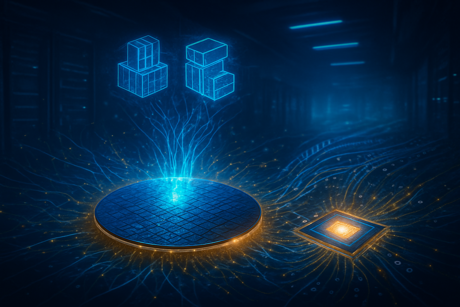
A Technical Rebirth: Copper-to-Copper Bonding and the Z-Angle Architecture
The technical underpinnings of Intel’s new strategy represent a radical departure from its previous GPU efforts. Eric Demers is reportedly overseeing a "clean-sheet" architecture that moves away from the multi-purpose legacy of the Xe and Arc lineups. Instead, the upcoming "Falcon Shores" and "Crescent Island" accelerators will utilize Intel’s 14A (1.4nm) process technology, specifically optimized for the matrix multiplication workloads essential for Generative AI. By prioritizing a "customer-driven" model, Intel is co-designing interconnect and bandwidth specifications directly with hyperscalers, ensuring that the hardware meets the specific power-envelope and throughput requirements of modern cloud clusters.
Central to this hardware evolution is the newly announced Z-Angle Memory (ZAM) technology. Unlike current High Bandwidth Memory (HBM4), which relies on traditional microbumps and through-silicon vias (TSVs) to stack DRAM layers, ZAM utilizes a sophisticated copper-to-copper (Cu-Cu) hybrid bonding technique. This methodology creates a monolithic-like silicon block that significantly reduces the vertical height of the stack while improving thermal conductivity. The "Z-Angle" refers to a novel staggered interconnect topology where data paths are routed diagonally through the die stack, rather than in straight vertical lines, reducing signal interference and latency.
Initial performance targets for ZAM are aggressive, aiming for up to 3x the capacity of current HBM standards—with targets reaching 512GB per stack—while consuming nearly 50% less power. By integrating these ZAM stacks directly with GPUs using Intel’s Embedded Multi-Die Interconnect Bridge (EMIB), the company plans to provide a high-density, low-latency memory solution that can host massive Large Language Models (LLMs) entirely on-package. This architectural shift addresses the primary bottleneck of current AI accelerators: the energy-intensive and slow process of fetching data from off-chip memory.
Industry Impact: Hyperscalers and the End of the NVIDIA Monoculture
The business implications of Intel’s GPU reboot are immediate and far-reaching. For years, cloud giants like Microsoft (NASDAQ: MSFT) and Alphabet (NASDAQ: GOOGL) have sought viable alternatives to NVIDIA's Blackwell and Rubin architectures to reduce total cost of ownership (TCO) and mitigate supply chain dependencies. By adopting a "customer-driven" strategy, Lip-Bu Tan is positioning Intel as a flexible partner rather than a rigid vendor. This approach allows major AI labs and cloud providers to influence the silicon's design early in the development cycle, potentially leading to more efficient custom-tailored clusters that outperform generic off-the-shelf accelerators.
The collaboration with SoftBank also creates a powerful new alliance in the semiconductor ecosystem. As SoftBank continues its transition into an "AI-first" holding company, its investment in ZAM technology provides Intel with a guaranteed path to commercialization and a foothold in the Japanese and broader Asian markets. For NVIDIA and AMD, the entry of a reinvigorated Intel—armed with both a domestic foundry and a world-class GPU architect—represents the most credible threat to their market share in years. If Intel can successfully execute its 1.4nm roadmap alongside ZAM, the "NVIDIA tax" that has plagued the industry could begin to erode as competition intensifies.
Wider Significance: Sovereignty and the New Memory Paradigm
In the broader context of the AI landscape, Intel's move is a significant step toward domestic chip sovereignty. By leveraging its own U.S.-based foundries for the production of these high-end GPUs and memory stacks, Intel is aligning itself with global trends toward localized supply chains for critical technology. This "all-Intel" integration—from the transistors to the packaging to the memory—is a unique strategic advantage that few competitors can match. While others must rely on external foundries and standardized memory components, Intel’s vertically integrated model allows for a level of cross-optimization that could define the next era of high-performance computing.
The development of ZAM technology also highlights a shifting paradigm in AI research. As model sizes continue to balloon, the industry has reached a point where raw compute power is often secondary to memory efficiency. Intel’s focus on the "memory wall" suggests a future where AI breakthroughs are driven by how fast data can move within a chip rather than just how many FLOPS it can perform. This focus on "system-level" efficiency mirrors the evolution seen in previous computing eras, where breakthroughs in storage and RAM often preceded the next major jump in software capability.
Future Outlook: Prototypes, Processes, and the 2027 Horizon
Looking ahead, the road to commercialization for these new technologies is clear but challenging. Intel has scheduled the first prototypes of ZAM-equipped accelerators for 2027, with full-scale production expected by the end of the decade. In the near term, the market will be watching the first architectural "fingerprints" of Eric Demers on Intel’s 2026 product refreshes. His influence is expected to streamline the software stack—long a point of contention for Intel’s GPU division—by unifying the OneAPI framework with a more robust, developer-friendly interface that rivals NVIDIA’s CUDA.
The next twelve to eighteen months will be a critical testing period. Intel must demonstrate that its 14A process can deliver the promised yields and that the "customer-driven" designs actually result in superior TCO for hyperscalers. If these milestones are met, analysts predict a significant shift in data center procurement cycles by 2028. However, the technical complexity of copper-to-copper hybrid bonding remains a hurdle, and Intel will need to prove it can manufacture these advanced packages at a scale that satisfies the insatiable global demand for AI compute.
A New Chapter for the Silicon Giant
Intel's latest moves represent a comprehensive strategy to reclaim its position at the center of the computing universe. By pairing the architectural genius of Eric Demers with a revolutionary memory technology in ZAM, CEO Lip-Bu Tan has laid the groundwork for a sustained assault on the high-end GPU market. This is no longer just a peripheral business for Intel; it is a fundamental reconfiguration of the company's DNA, shifting from a processor-first mindset to an AI-system-first architecture.
The significance of this moment in AI history cannot be overstated. We are witnessing the maturation of the AI hardware market from a one-player dominance to a multi-polar competitive landscape. For enterprise customers, this means more choice, lower costs, and faster innovation. For Intel, it is a high-stakes gamble that could either cement its legacy as the ultimate turnaround story or mark its final attempt to keep pace with the exponential growth of the AI era. In the coming weeks, eyes will be on the first engineering samples and the further expansion of the ZAM partnership as the industry prepares for the next phase of the AI revolution.
This content is intended for informational purposes only and represents analysis of current AI developments.
TokenRing AI delivers enterprise-grade solutions for multi-agent AI workflow orchestration, AI-powered development tools, and seamless remote collaboration platforms.
For more information, visit https://www.tokenring.ai/.