At the 2026 Consumer Electronics Show (CES), NVIDIA (NASDAQ: NVDA) dramatically shifted the landscape of autonomous transportation by unveiling "Alpamayo," a comprehensive open-source software stack designed to bring reasoning capabilities to self-driving vehicles. Named after the iconic Peruvian peak, Alpamayo marks a pivot for the chip giant from providing the underlying hardware "picks and shovels" to offering the intellectual blueprint for the future of physical AI. By open-sourcing the "brain" of the vehicle, NVIDIA aims to solve the industry’s most persistent hurdle: the "long-tail" of rare and complex edge cases that have prevented Level 4 autonomy from reaching the masses.
The announcement is being hailed as the "ChatGPT moment for physical AI," signaling a move away from the traditional, reactive "black box" AI systems that have dominated the industry for a decade. Rather than simply mapping pixels to steering commands, Alpamayo treats driving as a semantic reasoning problem, allowing vehicles to deliberate on human intent and physical laws in real-time. This transparency is expected to accelerate the development of autonomous fleets globally, democratizing advanced self-driving technology that was previously the exclusive domain of a handful of tech giants.
The Architecture of Reasoning: Inside Alpamayo 1
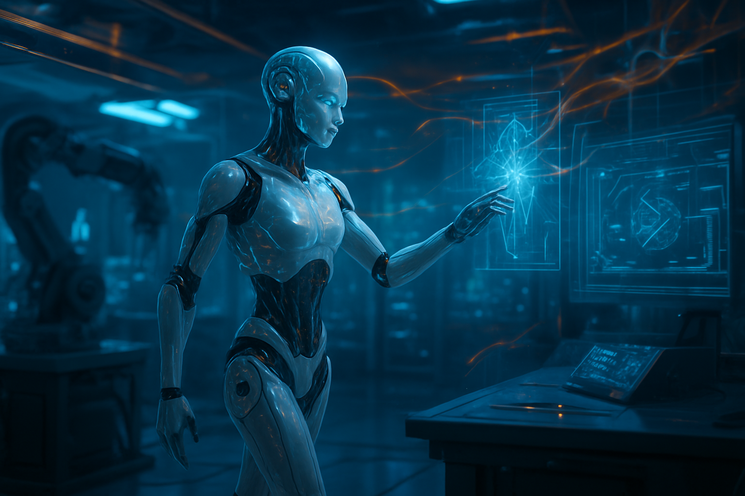
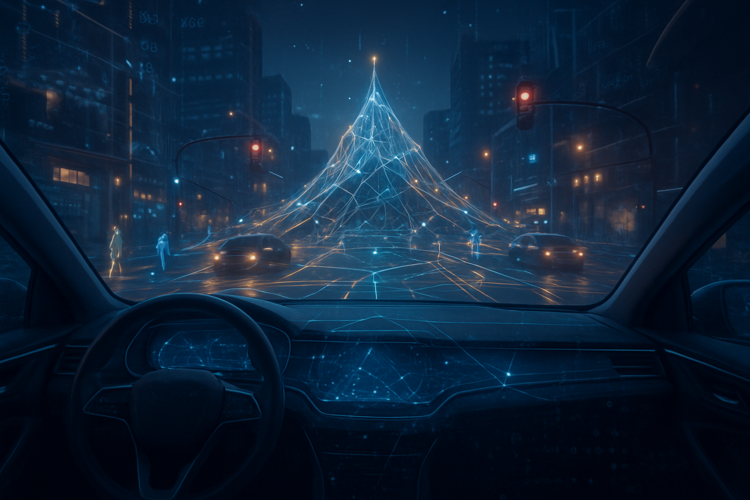
At the heart of the stack is Alpamayo 1, a 10-billion-parameter Vision-Language-Action (VLA) model. This foundation model is bifurcated into two distinct components: the 8.2-billion-parameter "Cosmos-Reason" backbone and a 2.3-billion-parameter "Action Expert." While previous iterations of self-driving software relied on pattern matching—essentially asking "what have I seen before that looks like this?"—Alpamayo utilizes "Chain-of-Causation" logic. The Cosmos-Reason backbone processes the environment semantically, allowing the vehicle to generate internal "logic logs." For example, if a child is standing near a ball on a sidewalk, the system doesn't just see a pedestrian; it reasons that the child may chase the ball into the street, preemptively adjusting its trajectory.
To support this reasoning engine, NVIDIA has paired the model with AlpaSim, an open-source simulation framework that utilizes neural reconstruction through Gaussian Splatting. This allows developers to take real-world camera data and instantly transform it into a high-fidelity 3D environment where they can "re-drive" scenes with different variables. If a vehicle encounters a confusing construction zone, AlpaSim can generate thousands of "what-if" scenarios based on that single event, teaching the AI how to handle novel permutations of the same problem. The stack is further bolstered by over 1,700 hours of curated "physical AI" data, gathered across 25 countries to ensure the model understands global diversity in infrastructure and human behavior.
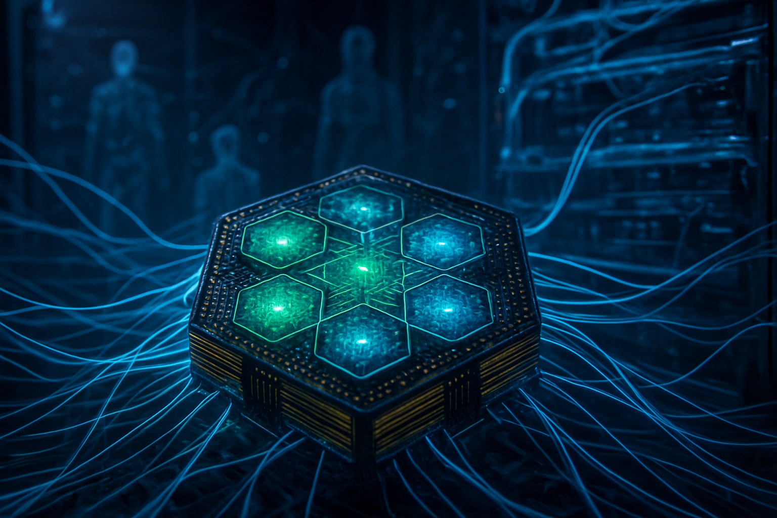
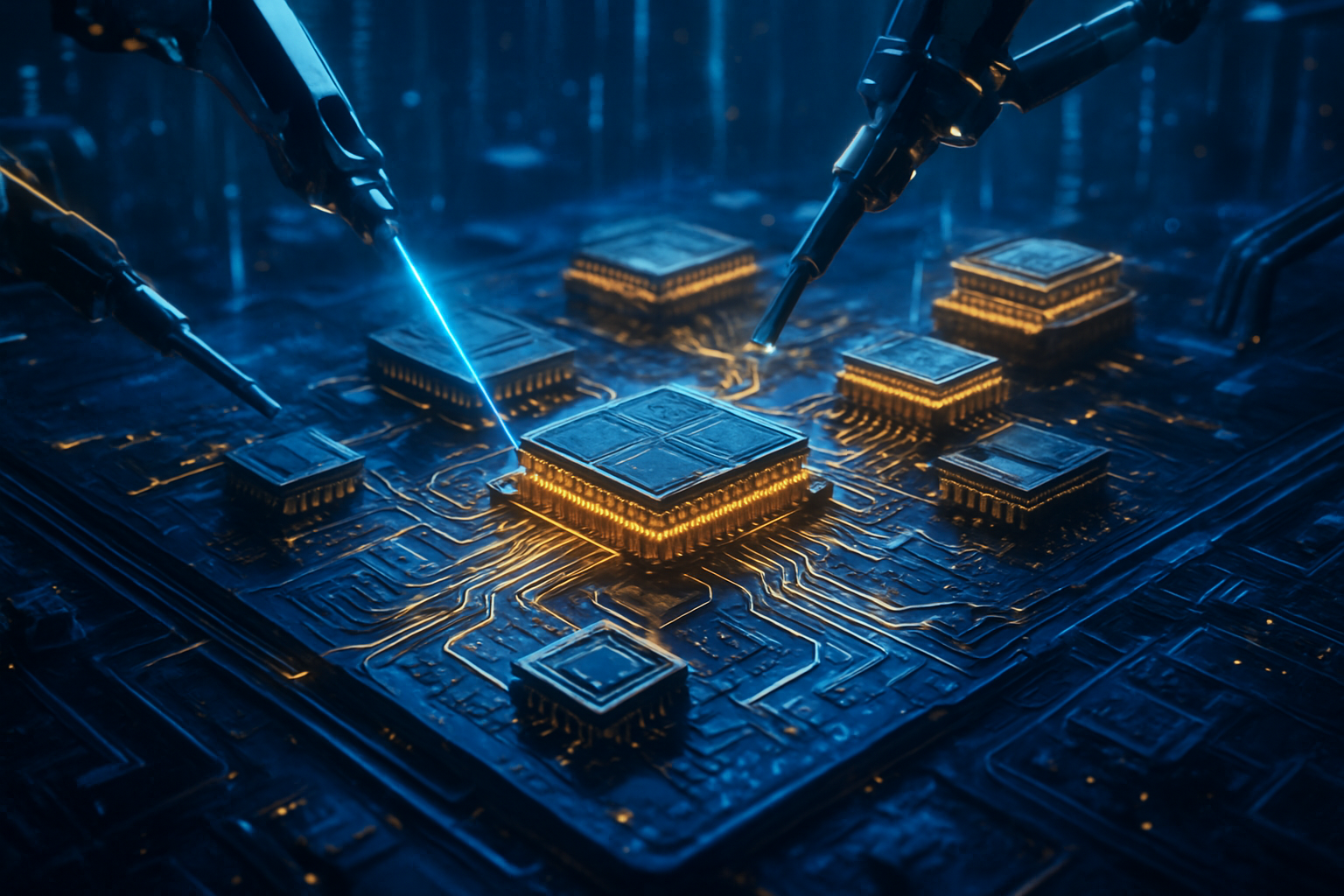
From a hardware perspective, Alpamayo is "extreme-codesigned" to run on the NVIDIA DRIVE Thor SoC, which utilizes the Blackwell architecture to deliver 508 TOPS of performance. For more demanding deployments, NVIDIA’s Hyperion platform can house dual-Thor configurations, providing the massive computational overhead required for real-time VLA inference. This tight integration ensures that the high-level reasoning of the teacher models can be distilled into high-performance runtime models that operate at a 10Hz frequency without latency—a critical requirement for high-speed safety.
Disrupting the Proprietary Advantage: A Challenge to Tesla and Beyond
The move to open-source Alpamayo is seen by market analysts as a direct challenge to the proprietary lead held by Tesla, Inc. (NASDAQ: TSLA). For years, Tesla’s Full Self-Driving (FSD) system has been considered the benchmark for end-to-end neural network driving. However, by providing a high-quality, open-source alternative, NVIDIA has effectively lowered the barrier to entry for the rest of the automotive industry. Legacy automakers who were struggling to build their own AI stacks can now adopt Alpamayo as a foundation, allowing them to skip a decade of research and development.
This strategic shift has already garnered significant industry support. Mercedes-Benz Group AG (OTC: MBGYY) has been named a lead partner, announcing that its 2026 CLA model will be the first production vehicle to integrate Alpamayo-derived teacher models for point-to-point navigation. Similarly, Uber Technologies, Inc. (NYSE: UBER) has signaled its intent to use the Alpamayo and Hyperion reference design for its next-generation robotaxi fleet, scheduled for a 2027 rollout. Other major players, including Lucid Group, Inc. (NASDAQ: LCID), Toyota Motor Corporation (NYSE: TM), and Stellantis N.V. (NYSE: STLA), have initiated pilot programs to evaluate how the stack can be integrated into their specific vehicle architectures.
The competitive implications are profound. If Alpamayo becomes the industry standard, the primary differentiator between car brands may shift from the "intelligence" of the driving software to the quality of the sensor suite and the luxury of the cabin experience. Furthermore, by providing "logic logs" that explain why a car made a specific maneuver, NVIDIA is addressing the regulatory and legal anxieties that have long plagued the sector. This transparency could shift the liability landscape, allowing manufacturers to defend their AI’s decisions in court using a "reasonable person" standard rather than being held to the impossible standard of a perfect machine.
Solving the Long-Tail: Broad Significance of Physical AI
The broader significance of Alpamayo lies in its approach to the "long-tail" problem. In autonomous driving, the first 95% of the task—staying in lanes, following traffic lights—was solved years ago. The final 5%, involving ambiguous hand signals from traffic officers, fallen debris, or extreme weather, has proven significantly harder. By treating these as reasoning problems rather than visual recognition tasks, Alpamayo brings "common sense" to the road. This shift aligns with the wider trend in the AI landscape toward multimodal models that can understand the physical laws of the world, a field often referred to as Physical AI.
However, the transition to reasoning-based systems is not without its concerns. Critics point out that while a model can "reason" on paper, the physical validation of these decisions remains a monumental task. The complexity of integrating such a massive software stack into the existing hardware of traditional OEMs (Original Equipment Manufacturers) could take years, leading to a "deployment gap" where the software is ready but the vehicles are not. Additionally, there are questions regarding the computational cost; while DRIVE Thor is powerful, running a 10-billion-parameter model in real-time remains an expensive endeavor that may initially be limited to premium vehicle segments.
Despite these challenges, Alpamayo represents a milestone in the evolution of AI. It moves the industry closer to a unified "foundation model" for the physical world. Just as Large Language Models (LLMs) changed how we interact with text, VLAs like Alpamayo are poised to change how machines interact with the three-dimensional space. This has implications far beyond cars, potentially serving as the operating system for humanoid robots, delivery drones, and automated industrial machinery.
The Road Ahead: 2026 and Beyond
In the near term, the industry will be watching the Q1 2026 rollout of the Mercedes-Benz CLA to see how Alpamayo performs in real-world consumer hands. The success of this launch will likely determine the pace at which other automakers commit to the stack. We can also expect NVIDIA to continue expanding the Alpamayo ecosystem, with rumors already circulating about a "Mini-Alpamayo" designed for lower-power edge devices and urban micro-mobility solutions like e-bikes and delivery bots.
The long-term vision for Alpamayo involves a fully interconnected ecosystem where vehicles "talk" to each other not just through position data, but through shared reasoning. If one vehicle encounters a road hazard and "reasons" a path around it, that logic can be shared across the cloud to all other Alpamayo-enabled vehicles in the vicinity. This collective intelligence could lead to a dramatic reduction in traffic accidents and a total optimization of urban transit. The primary challenge remains the rigorous safety validation required to move from L2+ "hands-on" systems to true L4 "eyes-off" autonomy in diverse regulatory environments.
A New Chapter for Autonomous Mobility
NVIDIA’s Alpamayo announcement marks a definitive end to the era of the "secretive AI" in the automotive sector. By choosing an open-source path, NVIDIA is betting that a transparent, collaborative ecosystem will reach Level 4 autonomy faster than any single company working in isolation. The shift from reactive pattern matching to deliberative reasoning is the most significant technical leap the industry has seen since the introduction of deep learning for computer vision.
As we move through 2026, the key metrics of success will be the speed of adoption by major OEMs and the reliability of the "Chain-of-Causation" logs in real-world scenarios. If Alpamayo can truly solve the "long-tail" through reasoning, the dream of a fully autonomous society may finally be within reach. For now, the tech world remains focused on the first fleet of Alpamayo-powered vehicles hitting the streets, as the industry begins to scale the steepest peak in AI development.
This content is intended for informational purposes only and represents analysis of current AI developments.
TokenRing AI delivers enterprise-grade solutions for multi-agent AI workflow orchestration, AI-powered development tools, and seamless remote collaboration platforms.
For more information, visit https://www.tokenring.ai/.