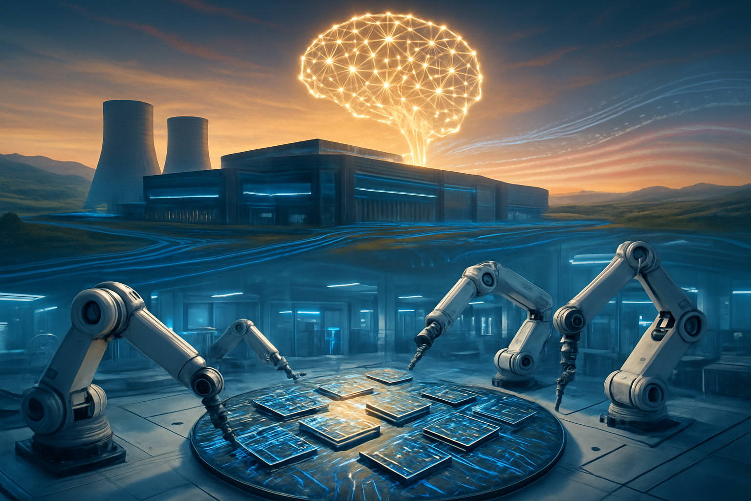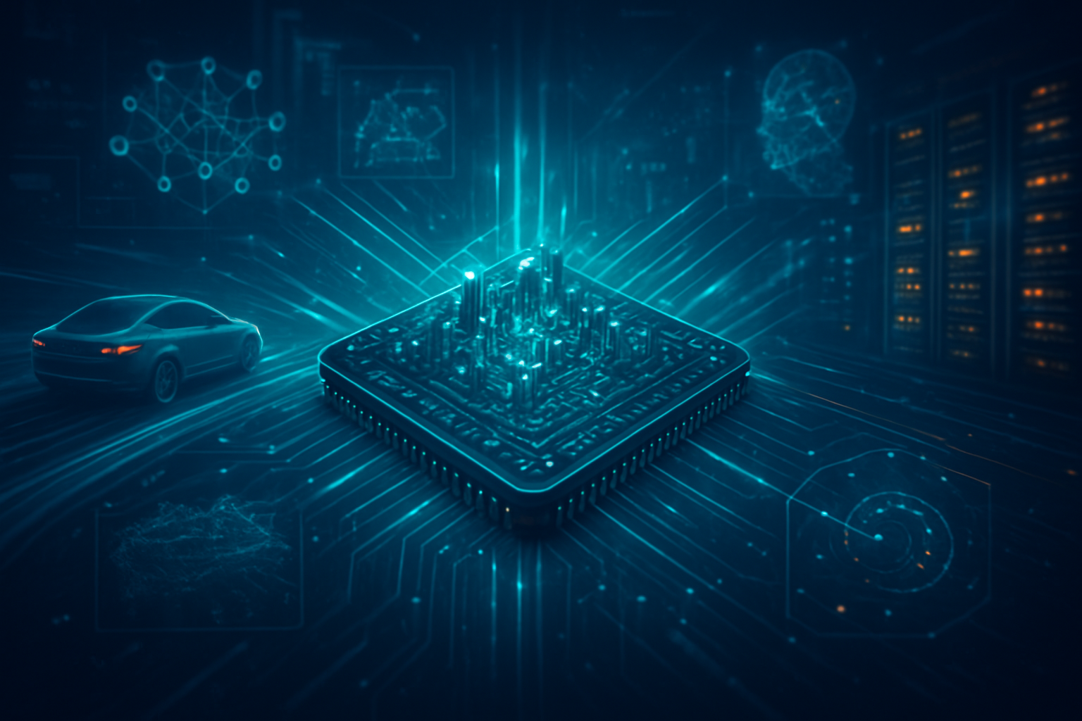
In a landmark shift that has redefined the trajectory of robotics and autonomous systems, NVIDIA (NASDAQ: NVDA) has solidified its dominance in the burgeoning field of "Physical AI." At the heart of this transformation is the NVIDIA Cosmos platform, a sophisticated suite of World Foundation Models (WFMs) that allows machines to perceive, reason about, and interact with the physical world with unprecedented nuance. Since its initial unveiling at CES 2025, Cosmos has rapidly evolved into the foundational "operating system" for the industry, solving the critical data scarcity problem that previously hindered the development of truly intelligent robots.
The immediate significance of Cosmos lies in its ability to bridge the "sim-to-real" gap—the notorious difficulty of moving an AI trained in a digital environment into the messy, unpredictable real world. By providing a generative AI layer that understands physics and causality, NVIDIA has effectively given machines a form of "digital common sense." As of January 2026, the platform is no longer just a research project; it is the core infrastructure powering a new generation of humanoid robots, autonomous delivery fleets, and Level 4 vehicle systems that are beginning to appear in urban centers across the globe.
Mastering the "Digital Matrix": Technical Specifications and Innovations
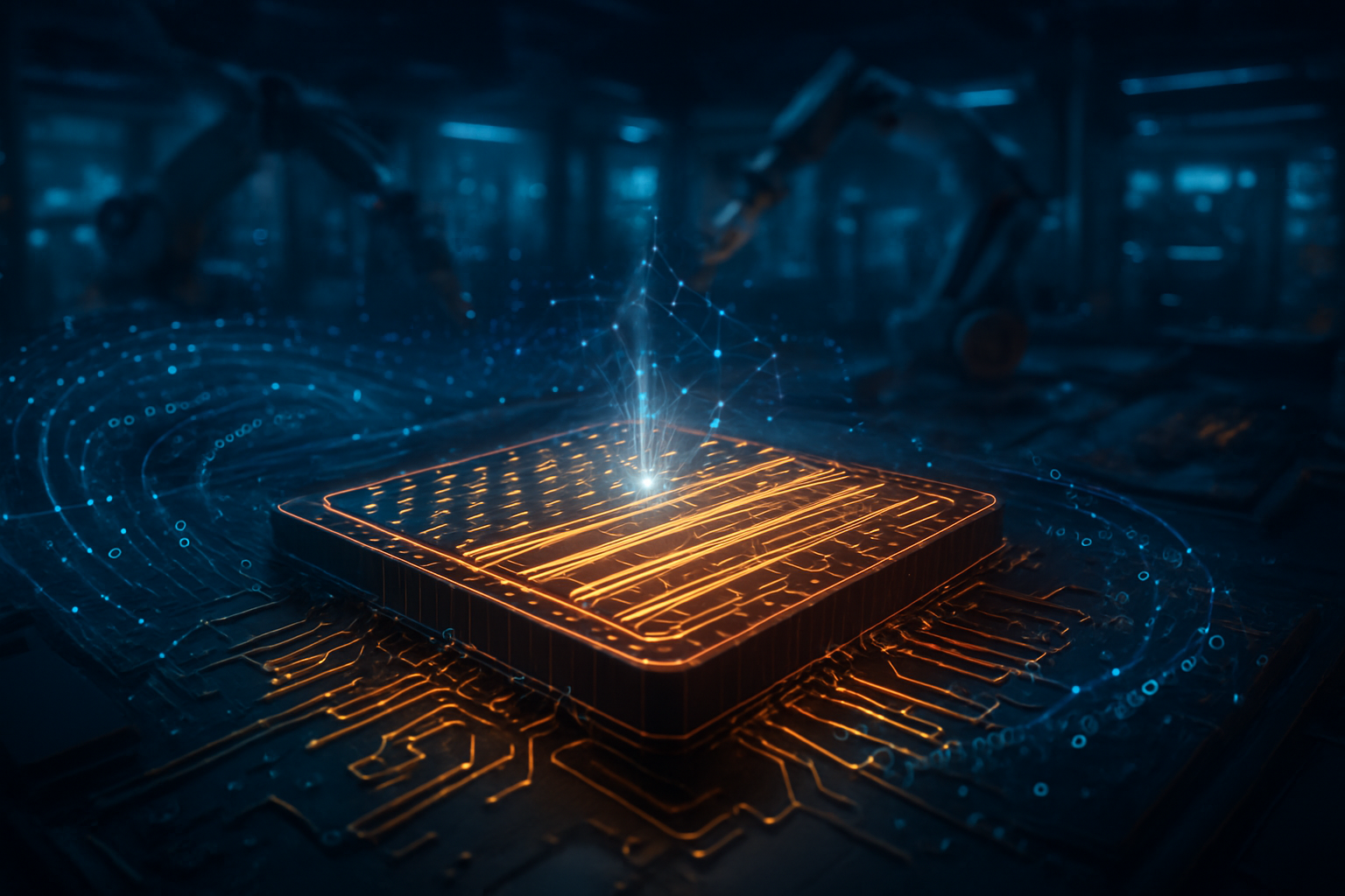
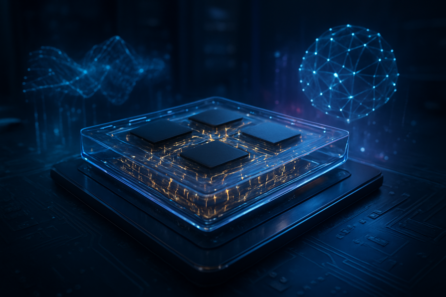
The NVIDIA Cosmos platform represents a departure from traditional simulation methods. While previous tools like NVIDIA Isaac Sim provided high-fidelity rendering and physics engines, Cosmos introduces a generative AI layer—the World Foundation Model. This model doesn't just render a scene; it "imagines" future states of the world. The technical stack is built on four pillars: the Cosmos Tokenizer, which compresses video data 8x more efficiently than previous standards; the Cosmos Curator, a GPU-accelerated pipeline capable of processing 20 million hours of video in a fraction of the time required by CPU-based systems; and the Cosmos Guardrails for safety.
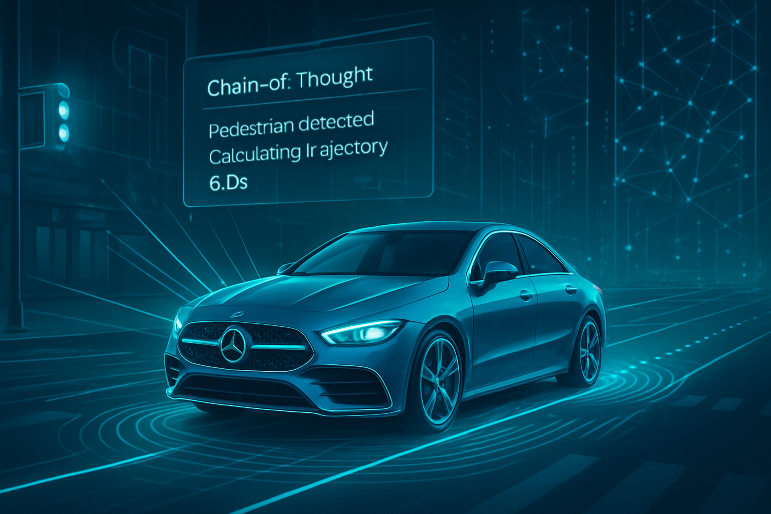
Central to the platform are three specialized model variants: Cosmos Predict, Cosmos Transfer, and Cosmos Reason. Predict serves as the robot’s "imagination," forecasting up to 30 seconds of high-fidelity physical outcomes based on potential actions. Transfer acts as the photorealistic bridge, converting structured 3D data into sensor-perfect video for training. Most notably, Cosmos Reason 2, unveiled earlier this month at CES 2026, is a vision-language model (VLM) with advanced spatio-temporal awareness. Unlike "black box" systems, Cosmos Reason can explain its logic in natural language, detailing why a robot chose to avoid a specific path or how it anticipates a collision before it occurs.
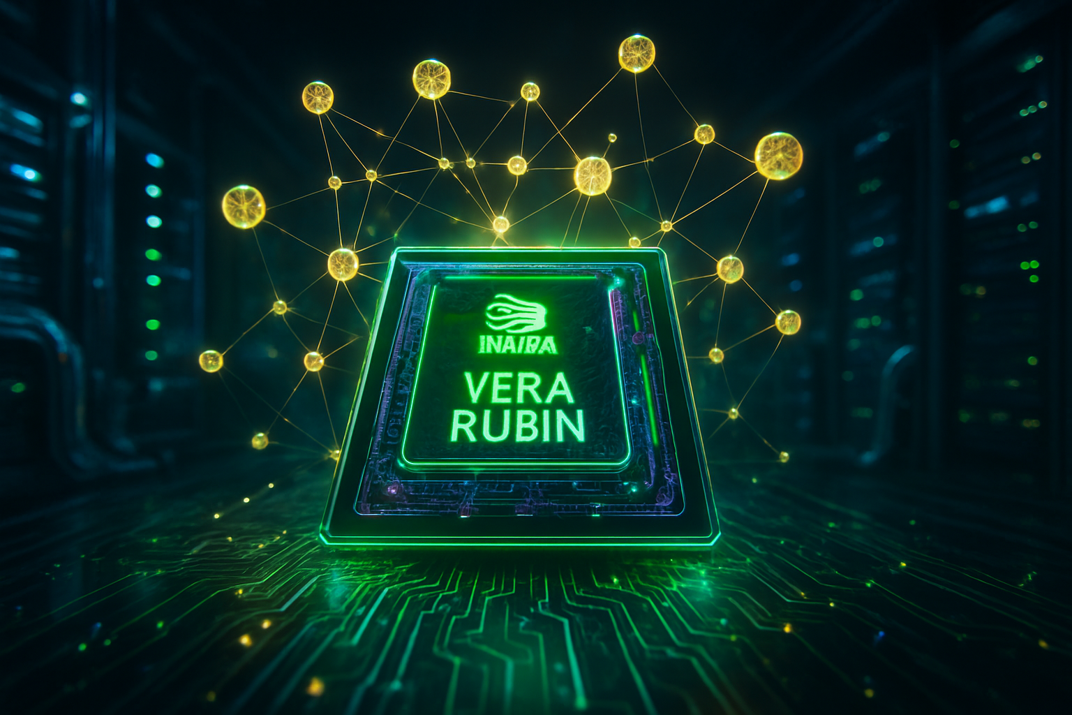
This architectural approach differs fundamentally from the "cyber-centric" models like GPT-4 or Claude. While those models excel at processing text and code, they lack an inherent understanding of gravity, friction, and object permanence. Cosmos models are trained on over 9,000 trillion tokens of physical data, including human-robot interactions and industrial environments. The recent transition to the Vera Rubin GPU architecture has further supercharged these capabilities, delivering a 12x improvement in tokenization speed and enabling real-time world generation on edge devices.
The Strategic Power Move: Reshaping the Competitive Landscape
NVIDIA’s strategy with Cosmos is frequently compared to the "Android" model of the mobile era. By providing a high-level intelligence layer to the entire industry, NVIDIA has positioned itself as the indispensable partner for nearly every major player in robotics. Startups like Figure AI and Agility Robotics have pivoted to integrate the Cosmos and Isaac GR00T stacks, moving away from more restricted partnerships. This "horizontal" approach contrasts sharply with Tesla (NASDAQ: TSLA), which continues to pursue a "vertical" strategy, relying on its proprietary end-to-end neural networks and massive fleet of real-world vehicles.
The competition is no longer just about who has the best hardware, but who has the best "World Model." While OpenAI remains a titan in digital reasoning, its Sora 2 video generation model now faces direct competition from Cosmos in the physical realm. Industry analysts note that NVIDIA’s "Three-Computer Strategy"—owning the cloud training (DGX), the digital twin (Omniverse), and the onboard inference (Thor/Rubin)—has created a massive ecosystem lock-in. Even as competitors like Waymo (NASDAQ: GOOGL) maintain a lead in safe, rule-based deployments, the industry trend is shifting toward the generative reasoning pioneered by Cosmos.
The strategic implications reached a fever pitch in late 2025 when Uber (NYSE: UBER) announced a massive partnership with NVIDIA to deploy a global fleet of 100,000 Level 4 robotaxis. By utilizing the Cosmos "Data Factory," Uber can simulate millions of rare edge cases—such as extreme weather or erratic pedestrian behavior—without the need for billions of miles of risky real-world testing. This has effectively allowed legacy manufacturers like Mercedes-Benz and BYD to leapfrog years of R&D, turning them into credible competitors to Tesla's Full Self-Driving (FSD) dominance.
Beyond the Screen: The Wider Significance of Physical AI
The rise of the Cosmos platform marks the transition from "Cyber AI" to "Embodied AI." If the previous era of AI was about organizing the world's information, this era is about organizing the world's actions. By creating an internal simulator that respects the laws of physics, NVIDIA is moving the industry toward machines that can truly coexist with humans in unconstrained environments. This development is seen as the "ChatGPT moment for robotics," providing the generalist foundation that was previously missing.
However, this breakthrough is not without its concerns. The energy requirements for training and running these world models are astronomical. Environmental critics point out that the massive compute power of the Rubin GPU architecture comes with a significant carbon footprint, sparking a debate over the sustainability of "Generalist AI." Furthermore, the "Liability Trap" remains a contentious issue; while NVIDIA provides the intelligence, the legal and ethical responsibility for accidents in the physical world remains with the vehicle and robot manufacturers, leading to complex regulatory discussions in Washington and Brussels.
Comparisons to previous milestones are telling. Where DeepBlue's victory over Garry Kasparov proved AI could master logic, and AlexNet proved it could master perception, Cosmos proves that AI can master the physical intuition of a toddler—the ability to understand that if a ball rolls into the street, a child might follow. This "common sense" layer is the missing piece of the puzzle for Level 5 autonomy and the widespread adoption of humanoid assistants in homes and hospitals.
The Road Ahead: What’s Next for Cosmos and Alpamayo
Looking toward the near future, the integration of the Alpamayo model—a reasoning-based vision-language-action (VLA) model built on Cosmos—is expected to be the next major milestone. Experts predict that by late 2026, we will see the first commercial deployments of robots that can perform complex, multi-stage tasks in homes, such as folding laundry or preparing simple meals, based purely on natural language instructions. The "Data Flywheel" effect will only accelerate as more robots are deployed, feeding real-world interaction data back into the Cosmos Curator.
One of the primary challenges that remains is the "last-inch" precision in manipulation. While Cosmos can predict physical outcomes, the hardware must still execute them with high fidelity. We are likely to see a surge in specialized "tactile" foundation models that focus specifically on the sense of touch, integrating directly with the Cosmos reasoning engine. As inference costs continue to drop with the refinement of the Rubin architecture, the barrier to entry for Physical AI will continue to fall, potentially leading to a "Cambrian Explosion" of robotic forms and functions.
Conclusion: A $5 Trillion Milestone
The ascent of NVIDIA to a $5 trillion market cap in early 2026 is perhaps the clearest indicator of the Cosmos platform's impact. NVIDIA is no longer just a chipmaker; it has become the architect of a new reality. By providing the tools to simulate the world, they have unlocked the ability for machines to navigate it. The key takeaway from the last year is that the path to true artificial intelligence runs through the physical world, and NVIDIA currently owns the map.
As we move further into 2026, the industry will be watching the scale of the Uber-NVIDIA robotaxi rollout and the performance of the first "Cosmos-native" humanoid robots in industrial settings. The long-term impact of this development will be measured by how seamlessly these machines integrate into our daily lives. While the technical hurdles are still significant, the foundation laid by the Cosmos platform suggests that the age of Physical AI has not just arrived—it is already accelerating.
This content is intended for informational purposes only and represents analysis of current AI developments.
TokenRing AI delivers enterprise-grade solutions for multi-agent AI workflow orchestration, AI-powered development tools, and seamless remote collaboration platforms.
For more information, visit https://www.tokenring.ai/.