Tag: Nvidia

  • The Colossus Awakening: xAI’s 555,000-GPU Supercluster and the Global Race for AGI Compute

    The Colossus Awakening: xAI’s 555,000-GPU Supercluster and the Global Race for AGI Compute

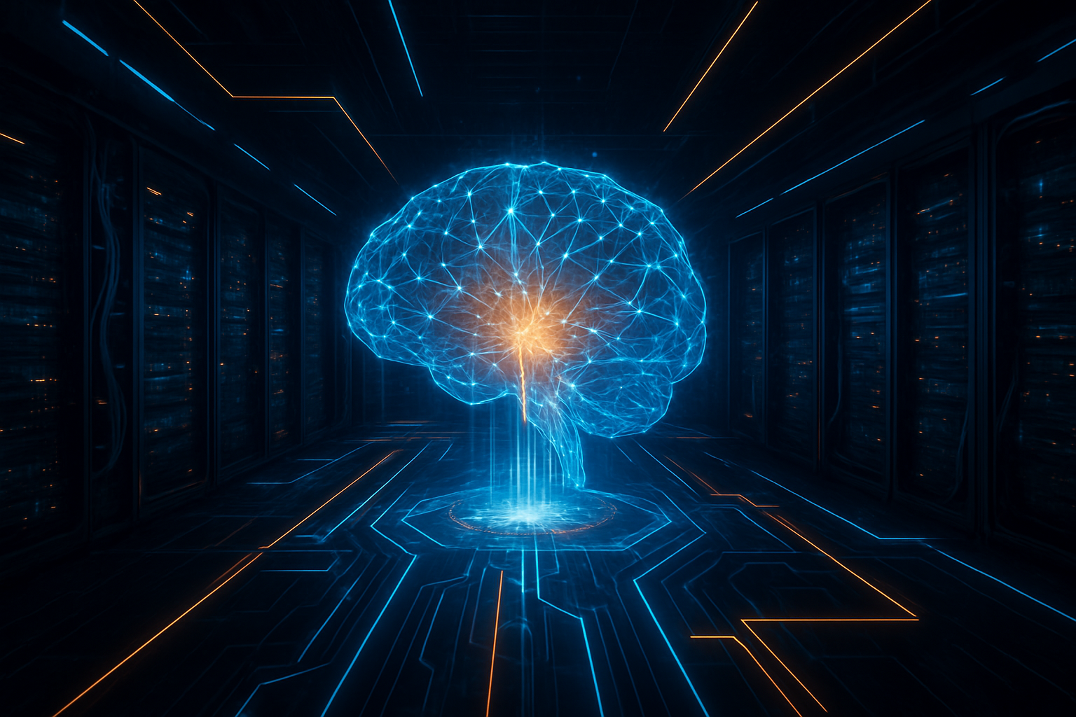
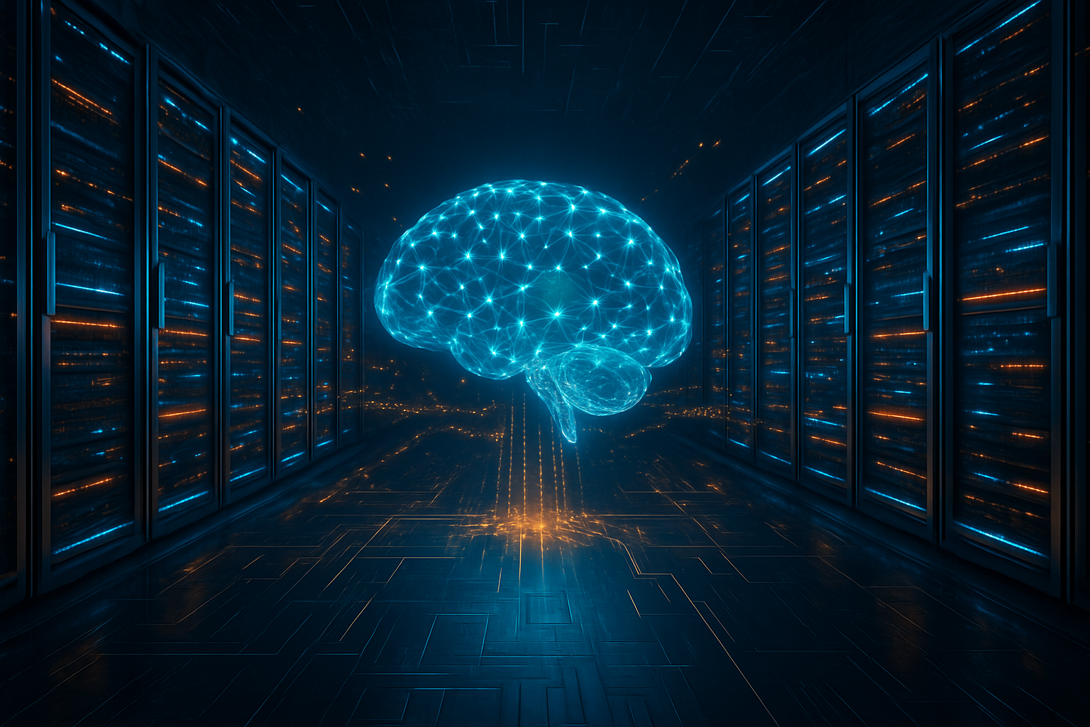
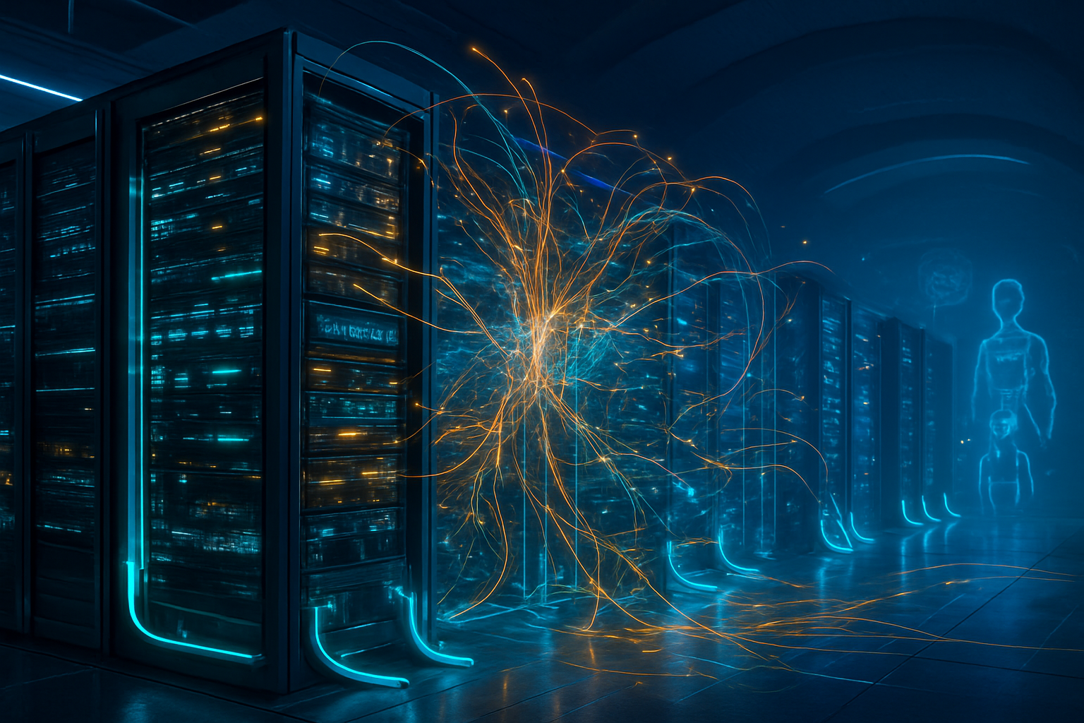
    In the heart of Memphis, Tennessee, a technological titan has reached its full stride. As of January 15, 2026, xAI’s "Colossus" supercluster has officially expanded to a staggering 555,000 GPUs, solidifying its position as the most concentrated burst of artificial intelligence compute on the planet. Built in a timeframe that has left traditional data center developers stunned, Colossus is not merely a server farm; it is a high-octane industrial engine designed for a singular purpose: training the next generation of Large Language Models (LLMs) to achieve what Elon Musk describes as "the dawn of digital superintelligence."

    The significance of Colossus extends far beyond its sheer size. It represents a paradigm shift in how AI infrastructure is conceived and executed. By bypassing the multi-year timelines typically associated with gigawatt-scale data centers, xAI has forced competitors to abandon cautious incrementalism in favor of "superfactory" deployments. This massive hardware gamble is already yielding dividends, providing the raw power behind the recently debuted Grok-3 and the ongoing training of the highly anticipated Grok-4 model.

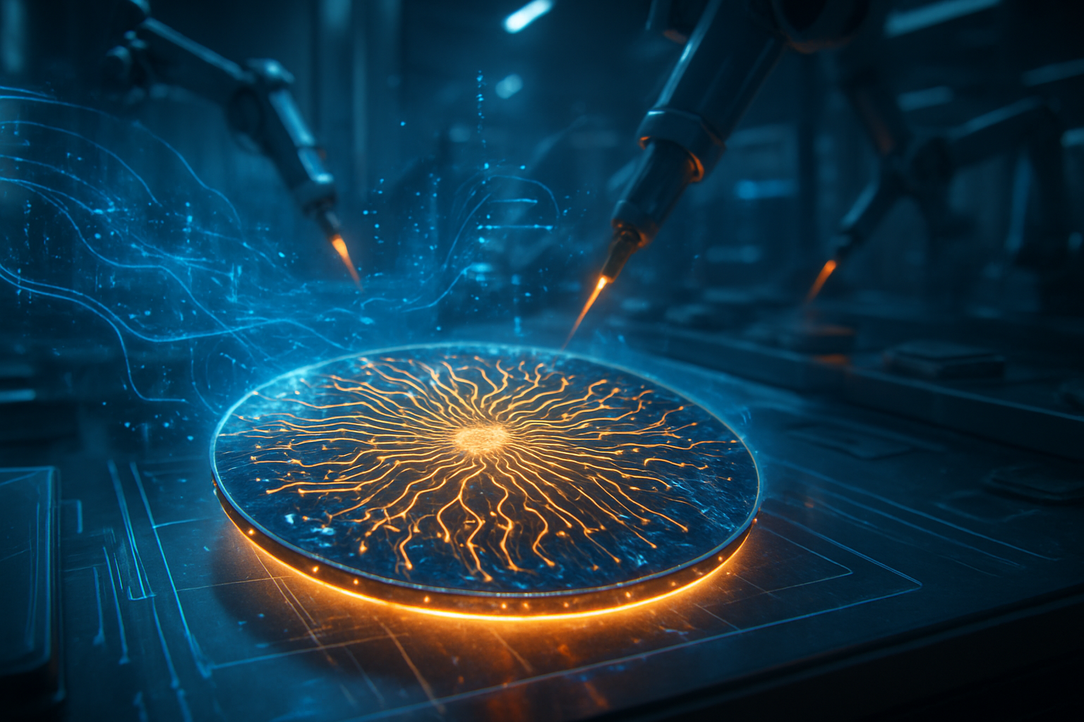
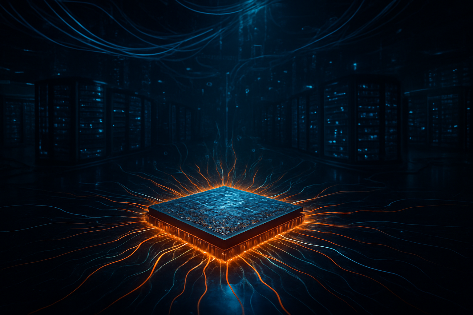
    The technical architecture of Colossus is a masterclass in extreme engineering. Initially launched in mid-2024 with 100,000 NVIDIA (NASDAQ: NVDA) H100 GPUs, the cluster underwent a hyper-accelerated expansion throughout 2025. Today, the facility integrates a sophisticated mix of NVIDIA’s H200 and the newest Blackwell GB200 and GB300 units. To manage the immense heat generated by over half a million chips, xAI partnered with Supermicro (NASDAQ: SMCI) to implement a direct-to-chip liquid-cooling (DLC) system. This setup utilizes redundant pump manifolds that circulate coolant directly across the silicon, allowing for unprecedented rack density that would be impossible with traditional air cooling.

    Networking remains the secret sauce of the Memphis site. Unlike many legacy supercomputers that rely on InfiniBand, Colossus utilizes NVIDIA’s Spectrum-X Ethernet platform equipped with BlueField-3 Data Processing Units (DPUs). Each server node is outfitted with 400GbE network interface cards, facilitating a total bandwidth of 3.6 Tbps per server. This high-throughput, low-latency fabric allows the cluster to function as a single, massive brain, updating trillions of parameters across the entire GPU fleet in less than a second—a feat necessary for the stable training of "Frontier" models that exceed current LLM benchmarks.

    This approach differs radically from previous generation clusters, which were often geographically distributed or limited by power bottlenecks. xAI solved the energy challenge through a hybrid power strategy, utilizing a massive array of 168+ Tesla (NASDAQ: TSLA) Megapacks. These batteries act as a giant buffer, smoothing out the massive power draws required during training runs and protecting the local Memphis grid from volatility. Industry experts have noted that the 122-day "ground-to-online" record for Phase 1 has set a new global benchmark, effectively cutting the standard industry deployment time by nearly 80%.

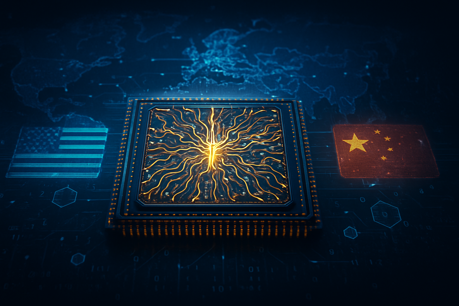
    The rapid ascent of Colossus has sent shockwaves through the competitive landscape, forcing a massive realignment among tech giants. Microsoft (NASDAQ: MSFT) and OpenAI, once the undisputed leaders in compute scale, have accelerated their "Project Stargate" initiative in response. As of early 2026, Microsoft’s first 450,000-GPU Blackwell campus in Abilene, Texas, has gone live, marking a direct challenge to xAI’s dominance. However, while Microsoft’s strategy leans toward a distributed "planetary computer" model, xAI’s focus on single-site density gives it a unique advantage in iteration speed, as engineers can troubleshoot and optimize the entire stack within a single physical campus.

    Other players are feeling the pressure to verticalize their hardware stacks to avoid the "NVIDIA tax." Google (NASDAQ: GOOGL) has doubled down on its proprietary TPU v7 "Ironwood" chips, which now power over 90% of its internal training workloads. By controlling the silicon, the networking (via optical circuit switching), and the software, Google remains the most power-efficient competitor in the race, even if it lacks the raw GPU headcount of Colossus. Meanwhile, Meta (NASDAQ: META) has pivoted toward "Compute Sovereignty," investing over $10 billion in its Hyperion cluster in Louisiana, which seeks to blend NVIDIA hardware with Meta’s in-house MTIA chips to drive down the cost of open-source model training.

    For xAI, the strategic advantage lies in its integration with the broader Musk ecosystem. By using Tesla’s energy storage expertise and borrowing high-speed manufacturing techniques from SpaceX, xAI has turned data center construction into a repeatable industrial process. This vertical integration allows xAI to move faster than traditional cloud providers, which are often bogged down by multi-vendor negotiations and complex regulatory hurdles. The result is a specialized "AI foundry" that can adapt to new chip architectures months before more bureaucratic competitors.

    The emergence of "superclusters" like Colossus marks the beginning of the Gigawatt Era of computing. We are no longer discussing data centers in terms of "megawatts" or "thousands of chips"; the conversation has shifted to regional power consumption comparable to medium-sized cities. This move toward massive centralization of compute raises significant questions about energy sustainability and the environmental impact of AI. While xAI has mitigated some local concerns through its use of on-site gas turbines and Megapacks, the long-term strain on the Tennessee Valley Authority’s grid remains a point of intense public debate.

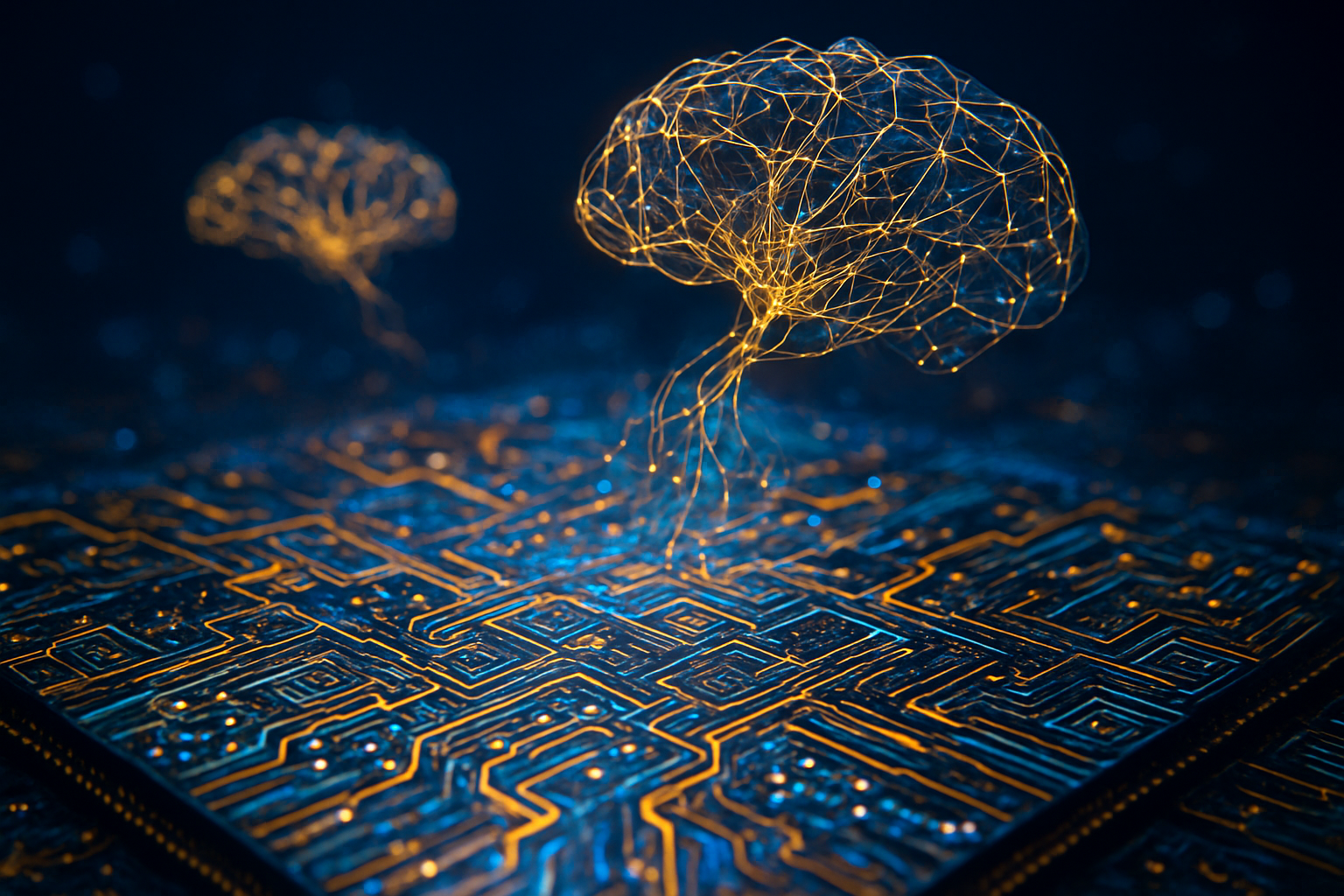
    In the broader AI landscape, Colossus represents the "industrialization" of intelligence. Much like the Manhattan Project or the Apollo program, the scale of investment—estimated to be well over $20 billion for the current phase—suggests that the industry believes the path to AGI (Artificial General Intelligence) is fundamentally a scaling problem. If "Scaling Laws" continue to hold, the massive compute advantage held by xAI could lead to a qualitative leap in reasoning and multi-modal capabilities that smaller labs simply cannot replicate, potentially creating a "compute moat" that stifles competition from startups.

    However, this centralization also brings risks. A single-site failure, whether due to a grid collapse or a localized disaster, could sideline the world's most powerful AI development for months. Furthermore, the concentration of such immense power in the hands of a few private individuals has sparked renewed calls for "compute transparency" and federal oversight. Comparisons to previous breakthroughs, like the first multi-core processors or the rise of cloud computing, fall short because those developments democratized access, whereas the supercluster race is currently concentrating power among the wealthiest entities on Earth.

    Looking toward the horizon, the expansion of Colossus is far from finished. Elon Musk has already teased the "MACROHARDRR" expansion, which aims to push the Memphis site toward 1 million GPUs by 2027. This next phase will likely see the first large-scale deployment of NVIDIA’s "Rubin" architecture, the successor to Blackwell, which promises even higher energy efficiency and memory bandwidth. Near-term applications will focus on Grok-5, which xAI predicts will be the first model capable of complex scientific discovery and autonomous engineering, moving beyond simple text generation into the realm of "agentic" intelligence.

    The primary challenge moving forward will be the "Power Wall." As clusters move toward 5-gigawatt requirements, traditional grid connections will no longer suffice. Experts predict that the next logical step for xAI and its rivals is the integration of small modular reactors (SMRs) or dedicated nuclear power plants directly on-site. Microsoft has already begun exploring this with the Three Mile Island restart, and xAI is rumored to be scouting locations with high nuclear potential for its Phase 4 expansion.

    As we move into late 2026, the focus will shift from "how many GPUs do you have?" to "how efficiently can you use them?" The development of new software frameworks that can handle the massive "jitter" and synchronization issues of 500,000+ chip clusters will be the next technical frontier. If xAI can master the software orchestration at this scale, the gap between "Frontier AI" and "Commodity AI" will widen into a chasm, potentially leading to the first verifiable instances of AGI-level performance in specialized domains like drug discovery and materials science.

    The Colossus supercluster is a monument to the relentless pursuit of scale. From its record-breaking construction in the Memphis suburbs to its current status as a 555,000-GPU behemoth, it serves as the definitive proof that the AI hardware race has entered a new, more aggressive chapter. The key takeaways are clear: speed-to-market is now as important as algorithmic innovation, and the winners of the AI era will be those who can command the most electrons and the most silicon in the shortest amount of time.

    In the history of artificial intelligence, Colossus will likely be remembered as the moment the "Compute Arms Race" went global and industrial. It has transformed xAI from an underdog startup into a heavyweight contender capable of staring down the world’s largest tech conglomerates. While the long-term societal and environmental impacts remain to be seen, the immediate reality is that the ceiling for what AI can achieve has been significantly raised by the sheer weight of the hardware in Tennessee.

    In the coming months, the industry will be watching the performance benchmarks of Grok-3 and Grok-4 closely. If these models demonstrate a significant lead over their peers, it will validate the "supercluster" strategy and trigger an even more frantic scramble for chips and power. For now, the world’s most powerful digital brain resides in Memphis, and its influence is only just beginning to be felt across the global tech economy.


    This content is intended for informational purposes only and represents analysis of current AI developments.

    TokenRing AI delivers enterprise-grade solutions for multi-agent AI workflow orchestration, AI-powered development tools, and seamless remote collaboration platforms.
    For more information, visit https://www.tokenring.ai/.

  • The Trillion-Dollar Handshake: Cisco AI Summit to Unite Jensen Huang and Sam Altman as Networking and GenAI Converge

    The Trillion-Dollar Handshake: Cisco AI Summit to Unite Jensen Huang and Sam Altman as Networking and GenAI Converge

    SAN FRANCISCO — January 15, 2026 — In what is being hailed as a defining moment for the "trillion-dollar AI economy," Cisco Systems (NASDAQ: CSCO) has officially confirmed the final agenda for its second annual Cisco AI Summit, scheduled to take place on February 3 in San Francisco. The event marks a historic shift in the technology landscape, featuring a rare joint appearance by NVIDIA (NASDAQ: NVDA) Founder and CEO Jensen Huang and OpenAI CEO Sam Altman. The summit signals the formal convergence of the two most critical pillars of the modern era: high-performance networking and generative artificial intelligence.

    For decades, networking was the "plumbing" of the internet, but as the industry moves toward 2026, it has become the vital nervous system for the "AI Factory." By bringing together the king of AI silicon and the architect of frontier models, Cisco is positioning itself as the indispensable bridge between massive GPU clusters and the enterprise applications that power the world. The summit is expected to unveil the next phase of the "Cisco Secure AI Factory," a full-stack architectural model designed to manufacture intelligence at a scale previously reserved for hyperscalers.

    The Technical Backbone: Nexus Meets Spectrum-X

    The technical centerpiece of this convergence is the deep integration between Cisco’s networking hardware and NVIDIA’s accelerated computing platform. Late in 2025, Cisco launched the Nexus 9100 series, the industry’s first third-party data center switch to natively integrate NVIDIA Spectrum-X Ethernet silicon technology. This integration allows Cisco switches to support "adaptive routing" and congestion control—features that were once exclusive to proprietary InfiniBand fabrics. By bringing these capabilities to standard Ethernet, Cisco is enabling enterprises to run large-scale Large Language Model (LLM) training and inference jobs with significantly reduced "Job Completion Time" (JCT).

    Beyond the data center, the summit will showcase the first real-world deployments of AI-Native Wireless (6G). Utilizing the NVIDIA AI Aerial platform, Cisco and NVIDIA have developed an AI-native wireless stack that integrates 5G/6G core software with real-time AI processing. This allows for "Agentic AI" at the edge, where devices can perform complex reasoning locally without the latency of cloud round-trips. This differs from previous approaches by treating the radio access network (RAN) and the AI compute as a single, unified fabric rather than separate silos.

    Industry experts from the AI research community have noted that this "unified fabric" approach addresses the most significant bottleneck in AI scaling: the "tails" of network latency. "We are moving away from building better switches to building a giant, distributed computer," noted Dr. Elena Vance, an independent networking analyst. Initial reactions suggest that Cisco's ability to provide a "turnkey" AI POD—combining Silicon One switches, NVIDIA HGX B300 GPUs, and VAST Data storage—is the competitive edge enterprises have been waiting for to move GenAI out of the lab and into mission-critical production.

    The Strategic Battle for the Enterprise AI Factory

    The strategic implications of this summit are profound, particularly for Cisco's market positioning. By aligning closely with NVIDIA and OpenAI, Cisco is making a direct play for the "back-end" network—the high-speed connections between GPUs—which was historically dominated by specialized players like Arista Networks (NYSE: ANET). For NVIDIA (NASDAQ: NVDA), the partnership provides a massive enterprise distribution channel, allowing them to penetrate corporate data centers that are already standardized on Cisco’s security and management software.

    For OpenAI, the collaboration with Cisco provides the physical infrastructure necessary for its ambitious "Stargate" project—a $100 billion initiative to build massive AI supercomputers. While Microsoft (NASDAQ: MSFT) remains OpenAI's primary cloud partner, the involvement of Sam Altman at a Cisco event suggests a diversification of infrastructure strategy, focusing on "sovereign AI" and private enterprise clouds. This move potentially disrupts the dominance of traditional public cloud providers by giving large corporations the tools to build their own "mini-Stargates" on-premises, maintained with Cisco’s security guardrails.

    Startups in the AI orchestration space also stand to benefit. By providing a standardized "AI Factory" template, Cisco is lowering the barrier to entry for developers to build multi-agent systems. However, companies specializing in niche networking protocols may find themselves squeezed as the Cisco-NVIDIA Ethernet standard becomes the default for enterprise AI. The strategic advantage here lies in "simplified complexity"—Cisco is effectively hiding the immense difficulty of GPU networking behind its familiar Nexus Dashboard.

    A New Era of Infrastructure and Geopolitics

    The convergence of networking and GenAI fits into a broader global trend of "AI Sovereignty." As nations and large enterprises become wary of relying solely on a few centralized cloud providers, the "AI Factory" model allows them to own their intelligence-generating infrastructure. This mirrors previous milestones like the transition to "Software-Defined Networking" (SDN), but with much higher stakes. If SDN was about efficiency, AI-native networking is about the very capability of a system to learn and adapt.

    However, this rapid consolidation of power between Cisco, NVIDIA, and OpenAI has raised concerns among some observers regarding "vendor lock-in" at the infrastructure layer. The sheer scale of the $100 billion letters of intent signed in late 2025 highlights the immense capital requirements of the AI age. We are witnessing a shift where networking is no longer a utility, but a strategic asset in a geopolitical race for AI dominance. The presence of Marc Andreessen and Dr. Fei-Fei Li at the summit underscores that this is not just a hardware update; it is a fundamental reconfiguration of the digital world.

    Comparisons are already being drawn to the early 1990s, when Cisco powered the backbone of the World Wide Web. Just as the router was the icon of the internet era, the "AI Factory" is becoming the icon of the generative era. The potential for "Agentic AI"—systems that can not only generate text but also take actions across a network—depends entirely on the security and reliability of the underlying fabric that Cisco and NVIDIA are now co-authoring.

    Looking Ahead: Stargate and Beyond

    In the near term, the February 3rd summit is expected to provide the first concrete updates on the "Stargate" international expansion, particularly in regions like the UAE, where Cisco Silicon One and NVIDIA Grace Blackwell systems are already being deployed. We can also expect to see the rollout of "Cisco AI Defense," a software suite that uses OpenAI’s models to monitor and secure LLM traffic in real-time, preventing data leakage and prompt injection attacks before they reach the network core.

    Long-term, the focus will shift toward the complete automation of network management. Experts predict that by 2027, "Self-Healing AI Networks" will be the standard, where the network identifies and fixes its own bottlenecks using predictive models. The challenge remains in the energy consumption of these massive clusters. Both Huang and Altman are expected to address the "power gap" during their keynotes, potentially announcing new liquid-cooling partnerships or high-efficiency silicon designs that further integrate compute and power management.

    The next frontier on the horizon is the integration of "Quantum-Safe" networking within the AI stack. As AI models become capable of breaking traditional encryption, the Cisco-NVIDIA alliance will likely need to incorporate post-quantum cryptography into their unified fabric to ensure that the "AI Factory" remains secure against future threats.

    Final Assessment: The Foundation of the Intelligence Age

    The Cisco AI Summit 2026 represents a pivotal moment in technology history. It marks the end of the "experimentation phase" of generative AI and the beginning of the "industrialization phase." By uniting the leaders in networking, silicon, and frontier models, the industry is creating a blueprint for how intelligence will be manufactured, secured, and distributed for the next decade.

    The key takeaway for investors and enterprise leaders is clear: the network is no longer separate from the AI. They are becoming one and the same. As Jensen Huang and Sam Altman take the stage together in San Francisco, they aren't just announcing products; they are announcing the architecture of a new economy. In the coming weeks, keep a close watch on Cisco’s "360 Partner Program" certifications and any further "Stargate" milestones, as these will be the early indicators of how quickly this trillion-dollar vision becomes a reality.


    This content is intended for informational purposes only and represents analysis of current AI developments.

    TokenRing AI delivers enterprise-grade solutions for multi-agent AI workflow orchestration, AI-powered development tools, and seamless remote collaboration platforms.
    For more information, visit https://www.tokenring.ai/.

  • Silicon Dominance: TSMC Shatters Records as AI Gold Rush Fuels Unprecedented Q4 Surge

    Silicon Dominance: TSMC Shatters Records as AI Gold Rush Fuels Unprecedented Q4 Surge

    In a definitive signal that the artificial intelligence revolution is only accelerating, Taiwan Semiconductor Manufacturing Company (NYSE: TSM) reported staggering record-breaking financial results for the fourth quarter of 2025. On January 15, 2026, the world’s largest contract chipmaker revealed that its quarterly net income surged 35% year-over-year to NT$505.74 billion (approximately US$16.01 billion), far exceeding analyst expectations and cementing its role as the indispensable foundation of the global AI economy.

    The results highlight a historic shift in the semiconductor landscape: for the first time, High-Performance Computing (HPC) and AI applications accounted for 58% of the company's annual revenue, officially dethroning the smartphone segment as TSMC’s primary growth engine. This "AI megatrend," as described by TSMC leadership, has pushed the company to a record quarterly revenue of US$33.73 billion, as tech giants scramble to secure the advanced silicon necessary to power the next generation of large language models and autonomous systems.

    The Push for 2nm and Beyond

    The technical milestones achieved in Q4 2025 represent a significant leap forward in Moore’s Law. TSMC officially announced the commencement of high-volume manufacturing (HVM) for its 2-nanometer (N2) process node at its Hsinchu and Kaohsiung facilities. The N2 node marks a radical departure from previous generations, utilizing the company’s first-generation nanosheet (Gate-All-Around or GAA) transistor architecture. This transition away from the traditional FinFET structure allows for a 10–15% increase in speed or a 25–30% reduction in power consumption compared to the already industry-leading 3nm (N3E) process.

    Furthermore, advanced technologies—classified as 7nm and below—now account for a massive 77% of TSMC’s total wafer revenue. The 3nm node has reached full maturity, contributing 28% of the quarter’s revenue as it powers the latest flagship mobile devices and AI accelerators. Industry experts have lauded TSMC’s ability to maintain a 62.3% gross margin despite the immense complexity of ramping up GAA architecture, a feat that competitors have struggled to match. Initial reactions from the research community suggest that the successful 2nm ramp-up effectively grants the AI industry a two-year head start on realizing complex "agentic" AI systems that require extreme on-chip efficiency.

    Market Implications for Tech Giants

    The implications for the "Magnificent Seven" and the broader startup ecosystem are profound. NVIDIA (NASDAQ: NVDA), the primary architect of the AI boom, remains TSMC’s largest customer for high-end AI GPUs, but the Q4 results show a diversifying base. Apple (NASDAQ: AAPL) has secured the lion’s share of initial 2nm capacity for its upcoming silicon, while Advanced Micro Devices (NASDAQ: AMD) and various hyperscalers developing custom ASICs—including Google's parent Alphabet (NASDAQ: GOOGL) and Amazon (NASDAQ: AMZN)—are aggressively vying for space on TSMC's production lines.

    TSMC’s strategic advantage is further bolstered by its massive expansion of CoWoS (Chip on Wafer on Substrate) advanced packaging capacity. By resolving the "packaging crunch" that bottlenecked AI chip supply throughout 2024 and early 2025, TSMC has effectively shortened the lead times for enterprise-grade AI hardware. This development places immense pressure on rival foundries like Intel (NASDAQ: INTC) and Samsung, who must now race to prove their own GAA implementations can achieve comparable yields. For startups, the increased supply of AI silicon means more affordable compute credits and a faster path to training specialized vertical models.

    The Global AI Landscape and Strategic Concerns

    Looking at the broader landscape, TSMC’s performance serves as a powerful rebuttal to skeptics who predicted an "AI bubble" burst in late 2025. Instead, the data suggests a permanent structural shift in global computing. The demand is no longer just for "training" chips but is increasingly shifting toward "inference" at scale, necessitating the high-efficiency 2nm and 3nm chips TSMC is uniquely positioned to provide. This milestone marks the first time in history that a single foundry has held such a critical bottleneck over the most transformative technology of a generation.

    However, this dominance brings significant geopolitical and environmental scrutiny. To mitigate concentration risks, TSMC confirmed it is accelerating its Arizona footprint, applying for permits for a fourth factory and its first U.S.-based advanced packaging plant. This move aims to create a "manufacturing cluster" in North America, addressing concerns about supply chain resilience in the Taiwan Strait. Simultaneously, the energy requirements of these advanced fabs remain a point of contention, as the power-hungry EUV (Extreme Ultraviolet) lithography machines required for 2nm production continue to challenge global sustainability goals.

    Future Roadmaps and 1.6nm Ambitions

    The roadmap for 2026 and beyond looks even more aggressive. TSMC announced a record-shattering capital expenditure budget of US$52 billion to US$56 billion for the coming year, with up to 80% dedicated to advanced process technologies. This investment is geared toward the upcoming N2P node, an enhanced version of the 2nm process, and the even more ambitious A16 (1.6-nanometer) node, which is slated for volume production in the second half of 2026. The A16 process will introduce backside power delivery, a technical revolution that separates the power circuitry from the signal circuitry to further maximize performance.

    Experts predict that the focus will soon shift from pure transistor density to "system-level" scaling. This includes the integration of high-bandwidth memory (HBM4) and sophisticated liquid cooling solutions directly into the chip packaging. The challenge remains the physical limits of silicon; as transistors approach the atomic scale, the industry must solve unprecedented thermal and quantum tunneling issues. Nevertheless, TSMC’s guidance of nearly 30% revenue growth for 2026 suggests they are confident in their ability to overcome these hurdles.

    Summary of the Silicon Era

    In summary, TSMC’s Q4 2025 earnings report is more than just a financial statement; it is a confirmation that the AI era is still in its high-growth phase. By successfully transitioning to 2nm GAA technology and significantly expanding its advanced packaging capabilities, TSMC has cleared the path for more powerful, efficient, and accessible artificial intelligence. The company’s record-breaking $16 billion quarterly profit is a testament to its status as the gatekeeper of modern innovation.

    In the coming weeks and months, the market will closely monitor the yields of the new 2nm lines and the progress of the Arizona expansion. As the first 2nm-powered consumer and enterprise products hit the market later this year, the gap between those with access to TSMC’s "leading-edge" silicon and those without will likely widen. For now, the global tech industry remains tethered to a single island, waiting for the next batch of silicon that will define the future of intelligence.


    This content is intended for informational purposes only and represents analysis of current AI developments.

    TokenRing AI delivers enterprise-grade solutions for multi-agent AI workflow orchestration, AI-powered development tools, and seamless remote collaboration platforms.
    For more information, visit https://www.tokenring.ai/.

  • The Great Re-Equilibrium: Trump Administration Reverses Course with Strategic Approval of NVIDIA H200 Exports to China

    The Great Re-Equilibrium: Trump Administration Reverses Course with Strategic Approval of NVIDIA H200 Exports to China

    In a move that has sent shockwaves through both Silicon Valley and the geopolitical corridors of Beijing, the Trump administration has officially rolled back key restrictions on high-end artificial intelligence hardware. Effective January 16, 2026, the U.S. Department of Commerce has issued a landmark policy update authorizing the export of the NVIDIA (NASDAQ: NVDA) H200 Tensor Core GPU to the Chinese market. The decision marks a fundamental departure from the previous administration’s "blanket ban" strategy, replacing it with a sophisticated "Managed Access" framework designed to maintain American technological dominance while re-establishing U.S. economic leverage.

    The policy shift is not a total liberalization of trade but rather a calculated gamble. Under the new rules, NVIDIA and other semiconductor leaders like AMD (NASDAQ: AMD) can sell their flagship Hopper-class and equivalent hardware to approved Chinese commercial entities, provided they navigate a gauntlet of new regulatory hurdles. By allowing these exports, the administration aims to blunt the rapid ascent of domestic Chinese AI chipmakers, such as Huawei, which had begun to monopolize the Chinese market in the absence of American competition.

    The Technical Leap: Restoring the Power Gap

    The technical implications of this policy are profound. For the past year, Chinese tech giants like Alibaba (NYSE: BABA) and ByteDance were restricted to the NVIDIA H20—a heavily throttled version of the Hopper architecture designed specifically to fall under the Biden-era performance caps. The H200, by contrast, is a powerhouse of the "Hopper" generation, boasting 141GB of HBM3e memory and a staggering 4.8 TB/s of bandwidth. Research indicates that the H200 is approximately 6.7 times faster for AI training tasks than the crippled H20 chips previously available in China.

    This "Managed Access" framework introduces three critical safeguards that differentiate it from pre-2022 trade:

    • The 25% "Government Cut": A mandatory tariff-style fee on every H200 sold to China, essentially turning high-end AI exports into a significant revenue stream for the U.S. Treasury.
    • Mandatory U.S. Routing: Every H200 destined for China must first be routed from fabrication sites in Taiwan to certified "Testing Hubs" in the United States. These labs verify that the hardware has not been tampered with or "overclocked" to exceed specified performance limits.
    • The 50% Volume Cap: Shipments to China are legally capped at 50% of the total volume sold to domestic U.S. customers, ensuring that American AI labs retain a hardware-availability advantage.

    Market Dynamics: A Windfall for Silicon Valley

    The announcement has had an immediate and electric effect on the markets. Shares of NVIDIA (NASDAQ: NVDA) surged 8% in pre-market trading, as analysts began recalculating the company’s "Total Addressable Market" (TAM) to include a Chinese demand surge that has been bottled up for nearly two years. For NVIDIA CEO Jensen Huang, the policy is a hard-won victory after months of lobbying for a "dependency model" rather than a "decoupling model." By supplying the H200, NVIDIA effectively resets the clock for Chinese developers, who might now abandon domestic alternatives like Huawei’s Ascend series in favor of the superior CUDA ecosystem.

    However, the competition is not limited to NVIDIA. The policy update also clears a path for AMD’s MI325X accelerators, sparking a secondary race between the two U.S. titans to secure long-term contracts with Chinese cloud providers. While the "Government Cut" will eat into margins, the sheer volume of anticipated orders from companies like Tencent (HKG: 0700) and Baidu (NASDAQ: BIDU) is expected to result in record-breaking quarterly revenues for the remainder of 2026. Startups in the U.S. AI space are also watching closely, as the 50% volume cap ensures that domestic supply remains a priority, preventing a price spike for local compute.

    Geopolitics: Dependency over Decoupling

    Beyond the balance sheets, the Trump administration's move signals a strategic pivot in the "AI Cold War." By allowing China access to the H200—but not the state-of-the-art "Blackwell" (B200) or the upcoming "Rubin" architectures—the U.S. is attempting to create a permanent "capability gap." The goal is to keep China’s AI ecosystem tethered to American software and hardware standards, making it difficult for Beijing to achieve true technological self-reliance.

    This approach acknowledges the reality that strict bans were accelerating China’s domestic innovation. Experts from the AI research community have noted that while the H200 will allow Chinese firms to train significantly larger models than before, they will still remain 18 to 24 months behind the frontier models being trained in the U.S. on Blackwell-class clusters. Critics, however, warn that the H200 is still more than capable of powering advanced surveillance and military-grade AI, raising questions about whether the 25% tariff is a sufficient price for the potential national security risks.

    The Horizon: What Comes After Hopper?

    Looking ahead, the "Managed Access" policy creates a roadmap for how future hardware generations might be handled. The Department of Commerce has signaled that as "Rubin" chips become the standard in the U.S., the currently restricted "Blackwell" architecture might eventually be moved into the approved export category for China. This "rolling release" strategy ensures that the U.S. always maintains a one-to-two generation lead in hardware capabilities.

    The next few months will be a testing ground for the mandatory U.S. routing and testing hubs. If the logistics of shipping millions of chips through U.S. labs prove too cumbersome, it could lead to supply chain bottlenecks. Furthermore, the world is waiting for Beijing’s official response. While Chinese firms are desperate for the hardware, the 25% "tax" to the U.S. government and the intrusive testing requirements may be seen as a diplomatic affront, potentially leading to retaliatory measures on raw materials like gallium and germanium.

    A New Chapter in AI Governance

    The approval of NVIDIA H200 exports to China marks the end of the "Total Ban" era and the beginning of a "Pragmatic Engagement" era. The Trump administration has bet that economic leverage and technological dependency are more powerful tools than isolation. By turning the AI arms race into a regulated, revenue-generating trade channel, the U.S. is attempting to control the speed of China’s development without fully severing the ties that bind the two largest economies.

    In the coming weeks, all eyes will be on the first shipments leaving U.S. testing facilities. Whether this policy effectively sustains American leadership or inadvertently fuels a Chinese AI resurgence remains to be seen. For now, NVIDIA and its peers are back in the game in China, but they are playing under a new and much more complex set of rules.


    This content is intended for informational purposes only and represents analysis of current AI developments.

    TokenRing AI delivers enterprise-grade solutions for multi-agent AI workflow orchestration, AI-powered development tools, and seamless remote collaboration platforms.
    For more information, visit https://www.tokenring.ai/.

  • The Great Compute Realignment: OpenAI Taps Google TPUs to Power the Future of ChatGPT

    The Great Compute Realignment: OpenAI Taps Google TPUs to Power the Future of ChatGPT

    In a move that has sent shockwaves through the heart of Silicon Valley, OpenAI has officially diversified its massive compute infrastructure, moving a significant portion of ChatGPT’s inference operations onto Google’s (NASDAQ: GOOGL) custom Tensor Processing Units (TPUs). This strategic shift, confirmed in late 2025 and accelerating into early 2026, marks the first time the AI powerhouse has looked significantly beyond its primary benefactor, Microsoft (NASDAQ: MSFT), for the raw processing power required to sustain its global user base of over 700 million monthly active users.

    The partnership represents a fundamental realignment of the AI power structure. By leveraging Google Cloud’s specialized hardware, OpenAI is not only mitigating the "NVIDIA tax" associated with the high cost of H100 and B200 GPUs but is also securing the low-latency capacity necessary for its next generation of "reasoning" models. This transition signals the end of the exclusive era of the OpenAI-Microsoft partnership and underscores a broader industry trend toward hardware diversification and "Silicon Sovereignty."

    The Rise of Ironwood: Technical Superiority and Cost Efficiency

    At the core of this transition is the mass deployment of Google’s 7th-generation TPU, codenamed "Ironwood." Introduced in late 2025, Ironwood was designed specifically for the "Age of Inference"—an era where the cost of running models (inference) has surpassed the cost of training them. Technically, the Ironwood TPU (v7) offers a staggering 4.6 PFLOPS of FP8 peak compute and 192GB of HBM3E memory, providing 7.38 TB/s of bandwidth. This represents a generational leap over the previous Trillium (v6) hardware and a formidable alternative to NVIDIA’s (NASDAQ: NVDA) Blackwell architecture.

    What truly differentiates the TPU stack for OpenAI is Google’s proprietary Optical Circuit Switching (OCS). Unlike traditional Ethernet-based GPU clusters, OCS allows OpenAI to link up to 9,216 chips into a single "Superpod" with 10x lower networking latency. For a model as complex as GPT-4o or the newer o1 "Reasoning" series, this reduction in latency is critical for real-time applications. Industry experts estimate that running inference on Google TPUs is approximately 20% to 40% more cost-effective than using general-purpose GPUs, a vital margin for OpenAI as it manages a burn rate projected to hit $17 billion this year.

    The AI research community has reacted with a mix of surprise and validation. For years, Google’s TPU ecosystem was viewed as a "walled garden" reserved primarily for its own Gemini models. OpenAI’s adoption of the XLA (Accelerated Linear Algebra) compiler—necessary to run code on TPUs—demonstrates that the software hurdles once favoring NVIDIA’s CUDA are finally being cleared by the industry’s most sophisticated engineering teams.

    A Blow to Exclusivity: Implications for Tech Giants

    The immediate beneficiaries of this deal are undoubtedly Google and Broadcom (NASDAQ: AVGO). For Google, securing OpenAI as a tenant on its TPU infrastructure is a massive validation of its decade-long investment in custom AI silicon. It effectively positions Google Cloud as the "clear number two" in AI infrastructure, breaking the narrative that Microsoft Azure was the only viable home for frontier models. Broadcom, which co-designs the TPUs with Google, also stands to gain significantly as the primary architect of the world's most efficient AI accelerators.

    For Microsoft (NASDAQ: MSFT), the development is a nuanced setback. While the "Stargate" project—a $500 billion multi-year infrastructure plan with OpenAI—remains intact, the loss of hardware exclusivity signals a more transactional relationship. Microsoft is transitioning from OpenAI’s sole provider to one of several "sovereign enablers." This shift allows Microsoft to focus more on its own in-house Maia 200 chips and the integration of AI into its software suite (Copilot), rather than just providing the "pipes" for OpenAI’s growth.

    NVIDIA (NASDAQ: NVDA), meanwhile, faces a growing challenge to its dominance in the inference market. While it remains the undisputed king of training with its upcoming Vera Rubin platform, the move by OpenAI and other labs like Anthropic toward custom ASICs (Application-Specific Integrated Circuits) suggests that the high margins NVIDIA has enjoyed may be nearing a ceiling. As the market moves from "scarcity" (buying any chip available) to "efficiency" (building the exact chip needed), specialized hardware like TPUs are increasingly winning the high-volume inference wars.

    Silicon Sovereignty and the New AI Landscape

    This infrastructure pivot fits into a broader global trend known as "Silicon Sovereignty." Major AI labs are no longer content with being at the mercy of hardware allocation cycles or high third-party markups. By diversifying into Google TPUs and planning their own custom silicon, OpenAI is following a path blazed by Apple with its M-series chips: vertical integration from the transistor to the transformer.

    The move also highlights the massive scale of the "AI Factories" now being constructed. OpenAI’s projected compute spending is set to jump to $35 billion by 2027. This scale is so vast that it requires a multi-vendor strategy to ensure supply chain resilience. No single company—not even Microsoft or NVIDIA—can provide the 10 gigawatts of power and the millions of chips OpenAI needs to achieve its goals for Artificial General Intelligence (AGI).

    However, this shift raises concerns about market consolidation. Only a handful of companies have the capital and the engineering talent to design and deploy custom silicon at this level. This creates a widening "compute moat" that may leave smaller startups and academic institutions unable to compete with the "Sovereign Labs" like OpenAI, Google, and Meta. Comparisons are already being drawn to the early days of the cloud, where a few dominant players captured the vast majority of the infrastructure market.

    The Horizon: Project Titan and Beyond

    Looking forward, the use of Google TPUs is likely a bridge to OpenAI’s ultimate goal: "Project Titan." This in-house initiative, partnered with Broadcom and TSMC, aims to produce OpenAI’s own custom inference accelerators by late 2026. These chips will reportedly be tuned specifically for "reasoning-heavy" workloads, where the model performs thousands of internal "thought" steps before generating an answer.

    As these custom chips go live, we can expect to see a new generation of AI applications that were previously too expensive to run at scale. This includes persistent AI agents that can work for hours on complex coding or research tasks, and more seamless, real-time multimodal experiences. The challenge will be managing the immense power requirements of these "AI Factories," with experts predicting that the industry will increasingly turn toward nuclear and other dedicated clean energy sources to fuel their 10GW targets.

    In the near term, we expect OpenAI to continue scaling its footprint in Google Cloud regions globally, particularly those with the newest Ironwood TPU clusters. This will likely be accompanied by a push for more efficient model architectures, such as Mixture-of-Experts (MoE), which are perfectly suited for the distributed memory architecture of the TPU Superpods.

    Conclusion: A Turning Point in AI History

    The decision by OpenAI to rent Google TPUs is more than a simple procurement deal; it is a landmark event in the history of artificial intelligence. It marks the transition of the industry from a hardware-constrained "gold rush" to a mature, efficiency-driven infrastructure era. By breaking the GPU monopoly and diversifying its compute stack, OpenAI has taken a massive step toward long-term sustainability and operational independence.

    The key takeaways for the coming months are clear: watch for the performance benchmarks of the Ironwood TPU v7 as it scales, monitor the progress of OpenAI’s "Project Titan" with Broadcom, and observe how Microsoft responds to this newfound competition within its own backyard. As of January 2026, the message is loud and clear: the future of AI will not be built on a single architecture, but on a diverse, competitive, and highly specialized silicon landscape.


    This content is intended for informational purposes only and represents analysis of current AI developments.

    TokenRing AI delivers enterprise-grade solutions for multi-agent AI workflow orchestration, AI-powered development tools, and seamless remote collaboration platforms.
    For more information, visit https://www.tokenring.ai/.

  • NVIDIA Blackwell Rollout: The 25x Efficiency Leap That Changed the AI Economy

    NVIDIA Blackwell Rollout: The 25x Efficiency Leap That Changed the AI Economy

    The full-scale deployment of NVIDIA (NASDAQ:NVDA) Blackwell architecture has officially transformed the landscape of artificial intelligence, moving the industry from a focus on raw training capacity to the massive-scale deployment of frontier inference. As of January 2026, the Blackwell platform—headlined by the B200 and the liquid-cooled GB200 NVL72—has achieved a staggering 25x reduction in energy consumption and cost for the inference of massive models, such as those with 1.8 trillion parameters.

    This milestone represents more than just a performance boost; it signifies a fundamental shift in the economics of intelligence. By making the cost of "thinking" dramatically cheaper, NVIDIA has enabled a new class of reasoning-heavy AI agents that can process complex, multi-step tasks with a speed and efficiency that was technically and financially impossible just eighteen months ago.

    At the heart of Blackwell’s efficiency gains is the second-generation Transformer Engine. This specialized hardware and software layer introduces support for FP4 (4-bit floating point) precision, which effectively doubles the compute throughput and memory bandwidth for inference compared to the previous H100’s FP8 standard. By utilizing lower precision without sacrificing accuracy in Large Language Models (LLMs), NVIDIA has allowed developers to run significantly larger models on smaller hardware footprints.

    The architectural innovation extends beyond the individual chip to the rack-scale level. The GB200 NVL72 system acts as a single, massive GPU, interconnecting 72 Blackwell GPUs via NVLink 5. This fifth-generation interconnect provides a bidirectional bandwidth of 1.8 TB/s per GPU—double that of the Hopper generation—slashing the communication latency that previously acted as a bottleneck for Mixture-of-Experts (MoE) models. For a 1.8-trillion parameter model, this configuration allows for real-time inference that consumes only 0.4 Joules per token, compared to the 10 Joules per token required by a similar H100 cluster.

    Initial reactions from the AI research community have been overwhelmingly positive, particularly regarding the architecture’s dedicated Decompression Engine. Researchers at leading labs have noted that the ability to retrieve and decompress data up to six times faster has been critical for the rollout of "agentic" AI models. These models, which require extensive "Chain-of-Thought" reasoning, benefit directly from the reduced latency, enabling users to interact with AI that feels genuinely responsive rather than merely predictive.

    The dominance of Blackwell has created a clear divide among tech giants and AI startups. Microsoft (NASDAQ:MSFT) has been a primary beneficiary, integrating Blackwell into its Azure ND GB200 V6 instances. This infrastructure currently powers the latest reasoning-heavy models from OpenAI, allowing Microsoft to offer unprecedented "thinking" capabilities within its Copilot ecosystem. Similarly, Google (NASDAQ:GOOGL) has deployed Blackwell across its Cloud A4X VMs, leveraging the architecture’s efficiency to expand its Gemini 2.0 and long-context multimodal services.

    For Meta Platforms (NASDAQ:META), the Blackwell rollout has been the backbone of its Llama 4 training and inference strategy. CEO Mark Zuckerberg has recently highlighted that Blackwell clusters have allowed Meta to reach a 1,000 tokens-per-second milestone for its 400-billion-parameter "Maverick" variant, bringing ultra-fast, high-reasoning AI to billions of users across its social apps. Meanwhile, Amazon (NASDAQ:AMZN) has utilized the platform to enhance its AWS Bedrock service, offering startups a cost-effective way to run frontier-scale models without the massive overhead typically associated with trillion-parameter architectures.

    This shift has also pressured competitors like AMD (NASDAQ:AMD) and Intel (NASDAQ:INTC) to accelerate their own roadmaps. While AMD’s Instinct MI350 series has found success in specific enterprise niches, NVIDIA’s deep integration of hardware, software (CUDA), and networking (InfiniBand and Spectrum-X) has allowed it to maintain a near-monopoly on high-end inference. The strategic advantage for Blackwell users is clear: they can serve 25 times more users or run models 25 times more complex for the same electricity budget, creating a formidable barrier to entry for those on older hardware.

    The broader significance of the Blackwell rollout lies in its impact on global energy consumption and the "Sovereign AI" movement. As governments around the world race to build their own national AI infrastructures, the 25x efficiency gain has become a matter of national policy. Reducing the power footprint of data centers allows nations to scale their AI capabilities without overwhelming their power grids, a factor that has led to massive Blackwell deployments in regions like the Middle East and Southeast Asia.

    Blackwell also marks the definitive end of the "Training Era" as the primary driver of GPU demand. While training remains critical, the sheer volume of tokens being generated by AI agents in 2026 means that inference now accounts for the majority of the market's compute cycles. NVIDIA’s foresight in optimizing Blackwell for inference—rather than just training throughput—has successfully anticipated this transition, solidifying AI's role as a pervasive utility rather than a niche research tool.

    Comparing this to previous milestones, Blackwell is being viewed as the "Broadband Era" of AI. Much like the transition from dial-up to high-speed internet allowed for the creation of video streaming and complex web apps, the transition from Hopper to Blackwell has allowed for the creation of "Physical AI" and autonomous researchers. However, the concentration of such efficient power in the hands of a few tech giants continues to raise concerns about market monopolization and the environmental impact of even "efficient" mega-scale data centers.

    Looking forward, the AI hardware race shows no signs of slowing down. Even as Blackwell reaches its peak adoption, NVIDIA has already unveiled its successor at CES 2026: the Rubin architecture (R100). Rubin is expected to transition into mass production by the second half of 2026, promising a further 5x leap in inference performance and the introduction of HBM4 memory, which will offer a staggering 22 TB/s of bandwidth.

    The next frontier will be the integration of these chips into "Physical AI"—the world of robotics and the NVIDIA Omniverse. While Blackwell was optimized for LLMs and reasoning, the Rubin generation is being marketed as the foundation for humanoid robots and autonomous factories. Experts predict that the next two years will see a move toward "Unified Intelligence," where the same hardware clusters seamlessly handle linguistic reasoning, visual processing, and physical motor control.

    In summary, the rollout of NVIDIA Blackwell represents a watershed moment in the history of computing. By delivering 25x efficiency gains for frontier model inference, NVIDIA has solved the immediate "inference bottleneck" that threatened to stall AI adoption in 2024 and 2025. The transition to FP4 precision and the success of liquid-cooled rack-scale systems like the GB200 NVL72 have set a new gold standard for data center architecture.

    As we move deeper into 2026, the focus will shift to how effectively the industry can utilize this massive influx of efficient compute. While the "Rubin" architecture looms on the horizon, Blackwell remains the workhorse of the modern AI economy. For investors, developers, and policymakers, the message is clear: the cost of intelligence is falling faster than anyone predicted, and the race to capitalize on that efficiency is only just beginning.


    This content is intended for informational purposes only and represents analysis of current AI developments.

    TokenRing AI delivers enterprise-grade solutions for multi-agent AI workflow orchestration, AI-powered development tools, and seamless remote collaboration platforms.
    For more information, visit https://www.tokenring.ai/.

  • The Reasoning Revolution: How OpenAI o3 Shattered the ARC-AGI Barrier and Redefined Intelligence

    The Reasoning Revolution: How OpenAI o3 Shattered the ARC-AGI Barrier and Redefined Intelligence

    In a milestone that many researchers predicted was still a decade away, the artificial intelligence landscape has undergone a fundamental shift from "probabilistic guessing" to "verifiable reasoning." At the heart of this transformation is OpenAI’s o3 model, a breakthrough that has effectively ended the era of next-token prediction as the sole driver of AI progress. By achieving a record-breaking 87.5% score on the Abstract Reasoning Corpus (ARC-AGI) benchmark, o3 has demonstrated a level of fluid intelligence that surpasses the average human score of 85%, signaling the definitive arrival of the "Reasoning Era."

    The significance of this development cannot be overstated. Unlike traditional Large Language Models (LLMs) that rely on pattern matching from vast datasets, o3’s performance on ARC-AGI proves it can solve novel, abstract puzzles it has never encountered during training. This leap has transitioned AI from a tool for content generation into a platform for genuine problem-solving, fundamentally changing how enterprises, researchers, and developers interact with machine intelligence as we enter 2026.

    From Prediction to Deliberation: The Technical Architecture of o3

    The core innovation of OpenAI o3 lies in its departure from "System 1" thinking—the fast, intuitive, and often error-prone processing typical of earlier models like GPT-4o. Instead, o3 utilizes what researchers call "System 2" thinking: a slow, deliberate, and logical planning process. This is achieved through a technique known as "test-time compute" or inference scaling. Rather than generating an answer instantly, the model is allocated a "thinking budget" during the response phase, allowing it to explore multiple reasoning paths, backtrack from logical dead ends, and self-correct before presenting a final solution.

    This shift in architecture is powered by large-scale Reinforcement Learning (RL) applied to the model’s internal "Chain of Thought." While previous iterations like the o1 series introduced basic reasoning capabilities, o3 has refined this process to a degree where it can tackle "Frontier Math" and PhD-level science problems with unprecedented accuracy. On the ARC-AGI benchmark—specifically designed by François Chollet to resist memorization—o3’s high-compute configuration reached 87.5%, a staggering jump from the 5% score recorded by GPT-4 in early 2024 and the 32% achieved by the first reasoning models in late 2024.

    Furthermore, o3 introduced "Deliberative Alignment," a safety framework where the model’s hidden reasoning tokens are used to monitor its own logic against safety guidelines. This ensures that even as the model becomes more autonomous and capable of complex planning, it remains bound by strict ethical constraints. The production version of o3 also features multimodal reasoning, allowing it to apply System 2 logic to visual inputs, such as complex engineering diagrams or architectural blueprints, within its hidden thought process.

    The Economic Engine of the Reasoning Era

    The arrival of o3 has sent shockwaves through the tech sector, creating new winners and forcing a massive reallocation of capital. Nvidia (NASDAQ: NVDA) has emerged as the primary beneficiary of this transition. As AI utility shifts from training size to "thinking tokens" during inference, the demand for high-performance GPUs like the Blackwell and Rubin architectures has surged. CEO Jensen Huang’s assertion that "Inference is the new training" has become the industry mantra, as enterprises now spend more on the computational power required for an AI to "think" through a problem than they do on the initial model development.

    Microsoft (NASDAQ: MSFT), OpenAI’s largest partner, has integrated these reasoning capabilities deep into its Copilot stack, offering a "Think Deeper" mode that leverages o3 for complex coding and strategic analysis. However, the sheer demand for the 10GW+ of power required to sustain these reasoning clusters has forced OpenAI to diversify its infrastructure. Throughout 2025, OpenAI signed landmark compute deals with Oracle (NYSE: ORCL) and even utilized Google Cloud under the Alphabet (NASDAQ: GOOGL) umbrella to manage the global rollout of o3-powered autonomous agents.

    The competitive landscape has also been disrupted by the "DeepSeek Shock" of early 2025, where the Chinese lab DeepSeek demonstrated that reasoning could be achieved with higher efficiency. This led OpenAI to release o3-mini and the subsequent o4-mini models, which brought "System 2" capabilities to the mass market at a fraction of the cost. This price war has democratized high-level reasoning, allowing even small startups to build agentic workflows that were previously the exclusive domain of trillion-dollar tech giants.

    A New Benchmark for General Intelligence

    The broader significance of o3’s ARC-AGI performance lies in its challenge to the skepticism surrounding Artificial General Intelligence (AGI). For years, critics argued that LLMs were merely "stochastic parrots" that would fail when faced with truly novel logic. By surpassing the human benchmark on ARC-AGI, o3 has provided the most robust evidence to date that AI is moving toward general-purpose cognition. This marks a turning point comparable to the 1997 defeat of Garry Kasparov by Deep Blue, but with the added dimension of linguistic and visual versatility.

    However, this breakthrough has also amplified concerns regarding the "black box" nature of AI reasoning. While the model’s Chain of Thought allows for better debugging, the sheer complexity of o3’s internal logic makes it difficult for humans to fully verify its steps in real-time. This has led to a renewed focus on AI interpretability and the potential for "reward hacking," where a model might find a technically correct but ethically questionable path to a solution.

    Comparing o3 to previous milestones, the industry sees a clear trajectory: if GPT-3 was the "proof of concept" and GPT-4 was the "utility era," then o3 is the "reasoning era." We are no longer asking if the AI knows the answer; we are asking how much compute we are willing to spend for the AI to find the answer. This transition has turned intelligence into a variable cost, fundamentally altering the economics of white-collar work and scientific research.

    The Horizon: From Reasoning to Autonomous Agency

    Looking ahead to the remainder of 2026, experts predict that the "Reasoning Era" will evolve into the "Agentic Era." The ability of models like o3 to plan and self-correct is the missing piece required for truly autonomous AI agents. We are already seeing the first wave of "Agentic Engineers" that can manage entire software repositories, and "Scientific Discovery Agents" that can formulate and test hypotheses in virtual laboratories. The near-term focus is expected to be on "Project Astra"-style real-world integration, where Alphabet's Gemini and OpenAI’s o-series models interact with physical environments through robotics and wearable devices.

    The next major hurdle remains the "Frontier Math" and "Deep Physics" barriers. While o3 has made significant gains, scoring over 25% on benchmarks that previously saw near-zero results, it still lacks the persistent memory and long-term learning capabilities of a human researcher. Future developments will likely focus on "Continuous Learning," where models can update their knowledge base in real-time without requiring a full retraining cycle, further narrowing the gap between artificial and biological intelligence.

    Conclusion: The Dawn of a New Epoch

    The breakthrough of OpenAI o3 and its dominance on the ARC-AGI benchmark represent more than just a technical achievement; they mark the dawn of a new epoch in human-machine collaboration. By proving that AI can reason through novelty rather than just reciting the past, OpenAI has fundamentally redefined the limits of what is possible with silicon. The transition to the Reasoning Era ensures that the next few years will be defined not by the volume of data we feed into machines, but by the depth of thought they can return to us.

    As we look toward the months ahead, the focus will shift from the models themselves to the applications they enable. From accelerating the transition to clean energy through materials science to solving the most complex bugs in global infrastructure, the "thinking power" of o3 is set to become the most valuable resource on the planet. The age of the reasoning machine is here, and the world will never look the same.


    This content is intended for informational purposes only and represents analysis of current AI developments.

    TokenRing AI delivers enterprise-grade solutions for multi-agent AI workflow orchestration, AI-powered development tools, and seamless remote collaboration platforms.
    For more information, visit https://www.tokenring.ai/.

  • The Trillion-Dollar Era: Global Semiconductor Revenue to Surpass $1T Milestone in 2026

    The Trillion-Dollar Era: Global Semiconductor Revenue to Surpass $1T Milestone in 2026

    As of mid-January 2026, the global semiconductor industry has reached a historic turning point. New data released this month confirms that total industry revenue is on a definitive path to surpass the $1 trillion milestone by the end of the year. This transition, fueled by a relentless expansion in artificial intelligence infrastructure, represents a seismic shift in the global economy, effectively rebranding silicon from a cyclical commodity into a primary global utility.

    According to the latest reports from Omdia and analysis provided by TechNode via UBS (NYSE:UBS), the market is expanding at a staggering annual growth rate of 40% in key segments. This acceleration is not merely a post-pandemic recovery but a structural realignment of the world’s technological foundations. With data centers, edge computing, and automotive systems now operating on an AI-centric architecture, the semiconductor sector has become the indispensable engine of modern civilization, mirroring the role that electricity played in the 20th century.

    The Technical Engine: High Bandwidth Memory and 2nm Precision

    The technical drivers behind this $1 trillion milestone are rooted in the massive demand for logic and memory Integrated Circuits (ICs). In particular, the shift toward AI infrastructure has triggered unprecedented price increases and volume demand for High Bandwidth Memory (HBM). As we enter 2026, the industry is transitioning to HBM4, which provides the necessary data throughput for the next generation of generative AI models. Market leaders like SK Hynix (KRX:000660) have seen their revenues surge as they secure over 70% of the market share for specialized memory used in high-end AI accelerators.

    On the logic side, the industry is witnessing a "node rush" as chipmakers move toward 2nm and 1.4nm fabrication processes. Taiwan Semiconductor Manufacturing Company (NYSE:TSM), commonly known as TSMC, has reported that advanced nodes—specifically those at 7nm and below—now account for nearly 60% of total foundry revenue, despite representing a smaller fraction of total units shipped. This concentration of value at the leading edge is a departure from previous decades, where mature nodes for consumer electronics drove the bulk of industry volume.

    The technical specifications of these new chips are tailored specifically for "data processing" rather than general-purpose computing. For the first time in history, data center and AI-related chips are expected to account for more than 50% of all semiconductor revenue in 2026. This focus on "AI-first" silicon allows for higher margins and sustained demand, as hyperscalers such as Microsoft, Google, and Amazon continue to invest hundreds of billions in capital expenditures to build out global AI clusters.

    The Dominance of the 'N-S-T' System and Corporate Winners

    The "trillion-dollar era" has solidified a new power structure in the tech world, often referred to by analysts as the "N-S-T system": NVIDIA (NASDAQ:NVDA), SK Hynix, and TSMC. NVIDIA remains the undisputed king of the AI era, with its market capitalization crossing the $4.5 trillion mark in early 2026. The company’s ability to command over 90% of the data center GPU market has turned it into a sovereign-level economic force, with its revenue for the 2025–2026 period alone projected to approach half a trillion dollars.

    The competitive implications for other major players are profound. Samsung Electronics (KRX:000660) is aggressively pivoting to regain its lead in the HBM and foundry space, with 2026 operating profits projected to hit record highs as it secures "Big Tech" customers for its 2nm production lines. Meanwhile, Intel (NASDAQ:INTC) and AMD (NASDAQ:AMD) are locked in a fierce battle to provide alternative AI architectures, with AMD’s Instinct series gaining significant traction in the open-source and enterprise AI markets.

    This growth has also disrupted the traditional product lifecycle. Instead of the two-to-three-year refresh cycles common in the PC and smartphone eras, AI hardware is seeing annual or even semi-annual updates. This rapid iteration creates a strategic advantage for companies with vertically integrated supply chains or those with deep, multi-year partnerships at the foundry level. The barrier to entry for startups has risen significantly, though specialized "AI-at-the-edge" startups are finding niches in the growing automotive and industrial automation sectors.

    Semiconductors as the New Global Utility

    The broader significance of this milestone cannot be overstated. By reaching $1 trillion in revenue, the semiconductor industry has officially moved past the "boom and bust" cycles of its youth. Industry experts now describe semiconductors as a "primary global utility." Much like the power grid or the water supply, silicon is now the foundational layer upon which all other economic activity rests. This shift has elevated semiconductor policy to the highest levels of national security and international diplomacy.

    However, this transition brings significant concerns regarding supply chain resilience and environmental impact. The power requirements of the massive data centers driving this revenue are astronomical, leading to a parallel surge in investments for green energy and advanced cooling technologies. Furthermore, the concentration of manufacturing power in a handful of geographic locations remains a point of geopolitical tension, as nations race to "onshore" fabrication capabilities to ensure their share of the trillion-dollar pie.

    When compared to previous milestones, such as the rise of the internet or the smartphone revolution, the AI-driven semiconductor era is moving at a much faster pace. While it took decades for the internet to reshape the global economy, the transition to an AI-centric semiconductor market has happened in less than five years. This acceleration suggests that the current growth is not a temporary bubble but a permanent re-rating of the industry's value to society.

    Looking Ahead: The Path to Multi-Trillion Dollar Revenues

    The near-term outlook for 2026 and 2027 suggests that the $1 trillion mark is merely a floor, not a ceiling. With the rollout of NVIDIA’s "Rubin" platform and the widespread adoption of 2nm technology, the industry is already looking toward a $1.5 trillion target by 2030. Potential applications on the horizon include fully autonomous logistics networks, real-time personalized medicine, and "sovereign AI" clouds managed by individual nation-states.

    The challenges that remain are largely physical and logistical. Addressing the "power wall"—the limit of how much electricity can be delivered to a single chip or data center—will be the primary focus of R&D over the next twenty-four months. Additionally, the industry must navigate a complex regulatory environment as governments seek to control the export of high-end AI silicon. Analysts predict that the next phase of growth will come from "embedded AI," where every household appliance, vehicle, and industrial sensor contains a dedicated AI logic chip.

    Conclusion: A New Era of Silicon Sovereignty

    The arrival of the $1 trillion semiconductor era in 2026 marks the beginning of a new chapter in human history. The sheer scale of the revenue—and the 40% growth rate driving it—confirms that the AI revolution is the most significant technological shift since the Industrial Revolution. Key takeaways from this milestone include the undisputed leadership of the NVIDIA-TSMC-SK Hynix ecosystem and the total integration of AI into the global economic fabric.

    As we move through 2026, the world will be watching to see how the industry manages its newfound status as a global utility. The decisions made by a few dozen CEOs and government officials regarding chip allocation and manufacturing will now have a greater impact on global stability than ever before. In the coming weeks and months, all eyes will be on the quarterly earnings of the "Magnificent Seven" and their chip suppliers to see if this unprecedented growth can sustain its momentum toward even greater heights.


    This content is intended for informational purposes only and represents analysis of current AI developments.

    TokenRing AI delivers enterprise-grade solutions for multi-agent AI workflow orchestration, AI-powered development tools, and seamless remote collaboration platforms.
    For more information, visit https://www.tokenring.ai/.

  • Apple Loses Priority: The iPhone Maker Faces Higher Prices and Capacity Struggles at TSMC Amid AI Boom

    Apple Loses Priority: The iPhone Maker Faces Higher Prices and Capacity Struggles at TSMC Amid AI Boom

    For over a decade, the semiconductor industry followed a predictable hierarchy: Apple (NASDAQ: AAPL) sat at the throne of Taiwan Semiconductor Manufacturing Company (TPE: 2330 / NYSE: TSM), commanding "first-priority" access to the world’s most advanced chip-making nodes. However, as of January 15, 2026, that hierarchy has been fundamentally upended. The insatiable demand for generative AI hardware has propelled NVIDIA (NASDAQ: NVDA) and AMD (NASDAQ: AMD) into a direct collision course with the iPhone maker, forcing Apple to fight for manufacturing capacity in a landscape where mobile devices are no longer the undisputed kings of silicon.

    The implications of this shift are immediate and profound. For the first time, sources within the supply chain indicate that Apple has been hit with its largest price hike in recent history for its upcoming A20 chips, while NVIDIA is on track to overtake Apple as TSMC’s largest revenue contributor. As AI GPUs grow larger and more complex, they are physically displacing the space on silicon wafers once reserved for the iPhone, signaling a "power shift" in the global foundry market that prioritizes the AI super-cycle over consumer electronics.

    The Technical Toll of the 2nm Transition

    The heart of Apple’s current struggle lies in the transition to the 2-nanometer (2nm or N2) manufacturing node. For the upcoming A20 chip, which is expected to power the next generation of flagship iPhones, Apple is transitioning from the established FinFET architecture to a new Gate-All-Around (GAA) nanosheet design. While GAA offers significant performance-per-watt gains, the technical complexity has sent manufacturing costs into the stratosphere. Industry analysts report that 2nm wafers are now priced at approximately $30,000 each—a staggering 50% increase from the $20,000 price tag of the 3nm generation. This spike translates to a per-chip cost of roughly $280 for the A20, nearly double the production cost of the previous A19 Pro.

    This technical hurdle is compounded by the sheer physical footprint of modern AI accelerators. While an Apple A20 chip occupies roughly 100-120mm² of silicon, NVIDIA’s latest Blackwell and Rubin-architecture GPUs are massive monsters near the "reticle limit," often exceeding 800mm². In terms of raw wafer utilization, a single AI GPU consumes as much physical space as six to eight mobile chips. As NVIDIA and AMD book hundreds of thousands of wafers to satisfy the global demand for AI training, they are effectively "crowding out" the room available for smaller mobile dies. The AI research community has noted that this physical displacement is the primary driver behind the current capacity crunch, as TSMC’s specialized advanced packaging facilities, such as Chip-on-Wafer-on-Substrate (CoWoS), are now almost entirely booked by AI chipmakers through late 2026.

    A Realignment of Corporate Power

    The economic reality of the "AI Super-cycle" is now visible on TSMC’s balance sheet. For years, Apple contributed over 25% of TSMC’s total revenue, granting it "exclusive" early access to new nodes. By early 2026, that share has dwindled to an estimated 16-20%, while NVIDIA has surged to account for 20% or more of the foundry's top line. This revenue "flip" has emboldened TSMC to demand higher prices from Apple, which no longer possesses the same leverage it did during the smartphone-dominant era of the 2010s. High-Performance Computing (HPC) now accounts for nearly 58% of TSMC's sales, while the smartphone segment has cooled to roughly 30%.

    This shift has significant competitive implications. Major AI labs and tech giants like Microsoft (NASDAQ: MSFT) and Google (NASDAQ: GOOGL) are the ultimate end-users of the NVIDIA and AMD chips taking up Apple's space. These companies are willing to pay a premium that far exceeds what the consumer-facing smartphone market can bear. Consequently, Apple is being forced to adopt a "me-too" strategy for its own M-series Ultra chips, competing for the same 3D packaging resources that NVIDIA uses for its H100 and H200 successors. The strategic advantage of being TSMC’s "only" high-volume client has evaporated, as Apple now shares the spotlight with a roster of AI titans whose budgets are seemingly bottomless.

    The Broader Landscape: From Mobile-First to AI-First

    This development serves as a milestone in the broader technological landscape, marking the official end of the "Mobile-First" era in semiconductor manufacturing. Historically, the most advanced nodes were pioneered by mobile chips because they demanded the highest power efficiency. Today, the priority has shifted toward raw compute density and AI throughput. The "first dibs" status Apple once held for every new node is being dismantled; reports from Taipei suggest that for the upcoming 1.6nm (A16) node scheduled for 2027, NVIDIA—not Apple—will be the lead customer. This is a historic demotion for Apple, which has utilized every major TSMC node launch to gain a performance lead over its smartphone rivals.

    The concerns among industry experts are centered on the rising cost of consumer technology. If Apple is forced to absorb $280 for a single processor, the retail price of flagship iPhones may have to rise significantly to maintain the company’s legendary margins. Furthermore, this capacity struggle highlights a potential bottleneck for the entire tech industry: if TSMC cannot expand fast enough to satisfy both the AI boom and the consumer electronics cycle, we may see extended product cycles or artificial scarcity for non-AI hardware. This mirrors previous silicon shortages, but instead of being caused by supply chain disruptions, it is being caused by a fundamental realignment of what the world wants to build with its limited supply of advanced silicon.

    Future Developments and the 1.6nm Horizon

    Looking ahead, the tension between Apple and the AI chipmakers is only expected to intensify as we approach 2027. The development of "angstrom-era" chips at the 1.6nm node will require even more capital-intensive equipment, such as High-NA EUV lithography machines from ASML (NASDAQ: ASML). Experts predict that NVIDIA’s "Feynman" GPUs will likely be the primary drivers of this node, as the return on investment for AI infrastructure remains higher than that of consumer devices. Apple may be forced to wait six months to a year after the node's debut before it can secure enough volume for a global iPhone launch, a delay that was unthinkable just three years ago.

    Furthermore, we are likely to see Apple pivot its architectural strategy. To mitigate the rising costs of monolithic dies on 2nm and 1.6nm, Apple may follow the lead of AMD and NVIDIA by moving toward "chiplet" designs for its high-end processors. By breaking a single large chip into smaller pieces that are easier to manufacture, Apple could theoretically improve yields and reduce its reliance on the most expensive parts of the wafer. However, this transition requires advanced 3D packaging—the very resource that is currently being monopolized by the AI industry.

    Conclusion: The End of an Era

    The news that Apple is "fighting" for capacity at TSMC is more than just a supply chain update; it is a signal that the AI boom has reached a level of dominance that can challenge even the world’s most powerful corporation. For over a decade, the relationship between Apple and TSMC was the most stable and productive partnership in tech. Today, that partnership is being tested by the sheer scale of the AI revolution, which demands more power, more silicon, and more capital than any smartphone ever could.

    The key takeaways are clear: the cost of cutting-edge silicon is rising at an unprecedented rate, and the priority for that silicon has shifted from the pocket to the data center. In the coming months, all eyes will be on Apple’s pricing strategy for the iPhone 18 Pro and whether the company can find a way to reclaim its dominance in the foundry, or if it will have to accept its new role as one of many "VIP" customers in the age of AI.


    This content is intended for informational purposes only and represents analysis of current AI developments.

    TokenRing AI delivers enterprise-grade solutions for multi-agent AI workflow orchestration, AI-powered development tools, and seamless remote collaboration platforms.
    For more information, visit https://www.tokenring.ai/.

  • Wells Fargo Crowns AMD the ‘New Chip King’ for 2026, Predicting Major Market Share Gains Over NVIDIA

    Wells Fargo Crowns AMD the ‘New Chip King’ for 2026, Predicting Major Market Share Gains Over NVIDIA

    The landscape of artificial intelligence hardware is undergoing a seismic shift as 2026 begins. In a blockbuster research note released on January 15, 2026, Wells Fargo analyst Aaron Rakers officially designated Advanced Micro Devices (NASDAQ: AMD) as his "top pick" for the year, boldly crowning the company as the "New Chip King." This upgrade signals a turning point in the high-stakes AI race, where AMD is no longer viewed as a secondary alternative to industry giant NVIDIA (NASDAQ: NVDA), but as a primary architect of the next generation of data center infrastructure.

    Rakers projects a massive 55% upside for AMD stock, setting a price target of $345.00. The core of this bullish outlook is the "Silicon Comeback"—a narrative driven by AMD’s rapid execution of its AI roadmap and its successful capture of market share from NVIDIA. As hyperscalers and enterprise giants seek to diversify their supply chains and optimize for the skyrocketing demands of AI inference, AMD’s aggressive release cadence and superior memory architectures have positioned it to potentially claim up to 20% of the AI accelerator market by 2027.

    The Technical Engine: From MI300 to the MI400 'Yottascale' Frontier

    The technical foundation of AMD’s surge lies in its "Instinct" line of accelerators, which has evolved at a breakneck pace. While the MI300X became the fastest-ramping product in the company’s history throughout 2024 and 2025, the recent deployment of the MI325X and the MI350X series has fundamentally altered the competitive landscape. The MI350X, built on the 3nm CDNA 4 architecture, delivers a staggering 35x increase in inference performance compared to its predecessors. This leap is critical as the industry shifts its focus from training massive models to the more cost-sensitive and volume-heavy task of running them in production—a domain where AMD's high-bandwidth memory (HBM) advantages shine.

    Looking toward the back half of 2026, the tech community is bracing for the MI400 series. This next-generation platform is expected to feature HBM4 memory with capacities reaching up to 432GB and a mind-bending 19.6TB/s of bandwidth. Unlike previous generations, the MI400 is designed for "Yottascale" computing, specifically targeting trillion-parameter models that require massive on-chip memory to minimize data movement and power consumption. Industry experts note that AMD’s decision to move to an annual release cadence has allowed it to close the "innovation gap" that previously gave NVIDIA an undisputed lead.

    Furthermore, the software barrier—long considered AMD’s Achilles' heel—has largely been dismantled. The release of ROCm 7.2 has brought AMD’s software ecosystem to a state of "functional parity" for the majority of mainstream AI frameworks like PyTorch and TensorFlow. This maturity allows developers to migrate workloads from NVIDIA’s CUDA environment to AMD hardware with minimal friction. Initial reactions from the AI research community suggest that the performance-per-dollar advantage of the MI350X is now impossible to ignore, particularly for large-scale inference clusters where AMD reportedly offers 40% better token-per-dollar efficiency than NVIDIA’s B200 Blackwell chips.

    Strategic Realignment: Hyperscalers and the End of the Monolith

    The rise of AMD is being fueled by a strategic pivot among the world’s largest technology companies. Microsoft (NASDAQ: MSFT), Meta (NASDAQ: META), and Oracle (NYSE: ORCL) have all significantly increased their orders for AMD Instinct platforms to reduce their total dependence on a single vendor. By diversifying their hardware providers, these hyperscalers are not only gaining leverage in pricing negotiations but are also insulating their massive capital expenditures from potential supply chain bottlenecks that have plagued the industry in recent years.

    Perhaps the most significant industry endorsement came from OpenAI, which recently secured a landmark deal to integrate AMD GPUs into its future flagship clusters. This move is a clear signal to the market that even the most cutting-edge AI labs now view AMD as a tier-one hardware partner. For startups and smaller AI firms, the availability of AMD hardware in the cloud via providers like Oracle Cloud Infrastructure (OCI) offers a more accessible and cost-effective path to scaling their operations. This "democratization" of high-end silicon is expected to spark a new wave of innovation in specialized AI applications that were previously cost-prohibitive.

    The competitive implications for NVIDIA are profound. While the Santa Clara-based giant remains the market leader and recently unveiled its formidable "Rubin" architecture at CES 2026, it is no longer operating in a vacuum. NVIDIA’s Blackwell architecture faced initial thermal and power-density challenges, which provided a window of opportunity that AMD’s air-cooled and liquid-cooled "Helios" rack-scale systems have exploited. The "Silicon Comeback" is as much about AMD’s operational excellence as it is about the market's collective desire for a healthy, multi-vendor ecosystem.

    A New Era for the AI Landscape: Sustainability and Sovereignty

    The broader significance of AMD’s ascension touches on two of the most critical trends in the 2026 AI landscape: energy efficiency and technological sovereignty. As data centers consume an ever-increasing share of the global power grid, AMD’s focus on performance-per-watt has become a key selling point. The MI400 series is rumored to include specialized "inference-first" silicon pathways that significantly reduce the carbon footprint of running large language models at scale. This aligns with the aggressive sustainability goals set by companies like Microsoft and Google.

    Furthermore, the shift toward AMD reflects a growing global movement toward "sovereign AI" infrastructure. Governments and regional cloud providers are increasingly wary of being locked into a proprietary software stack like CUDA. AMD’s commitment to open-source software through the ROCm initiative and its support for the UXL Foundation (Unified Acceleration Foundation) resonates with those looking to build independent, flexible AI capabilities. This movement mirrors previous shifts in the tech industry, such as the rise of Linux in the server market, where open standards eventually overcame closed, proprietary systems.

    Concerns do remain, however. While AMD has made massive strides, NVIDIA's deeply entrenched ecosystem and its move toward vertical integration (including its own networking and CPUs) still present a formidable moat. Some analysts worry that the "chip wars" could lead to a fragmented development landscape, where engineers must optimize for multiple hardware backends. Yet, compared to the silicon shortages of 2023 and 2024, the current environment of robust competition is viewed as a net positive for the pace of AI advancement, ensuring that hardware remains a catalyst rather than a bottleneck.

    The Road Ahead: What to Expect in 2026 and Beyond

    In the near term, all eyes will be on AMD’s quarterly earnings reports to see if the projected 55% upside begins to materialize in the form of record data center revenue. The full-scale rollout of the MI400 series later this year will be the ultimate test of AMD’s ability to compete at the absolute bleeding edge of "Yottascale" computing. Experts predict that if AMD can maintain its current trajectory, it will not only secure its 20% market share goal but could potentially challenge NVIDIA for the top spot in specific segments like edge AI and specialized inference clouds.

    Potential challenges remain on the horizon, including the intensifying race for HBM4 supply and the need for continued expansion of the ROCm developer base. However, the momentum is undeniably in AMD's favor. As trillion-parameter models become the standard for enterprise AI, the demand for high-capacity, high-bandwidth memory will only grow, playing directly into AMD’s technical strengths. We are likely to see more custom "silicon-as-a-service" partnerships where AMD co-designs chips with hyperscalers, further blurring the lines between hardware provider and strategic partner.

    Closing the Chapter on the GPU Monopoly

    The crowning of AMD as the "New Chip King" by Wells Fargo marks the end of the mono-chip era in artificial intelligence. The "Silicon Comeback" is a testament to Lisa Su’s visionary leadership and a reminder that in the technology industry, no lead is ever permanent. By focusing on the twin pillars of massive memory capacity and open-source software, AMD has successfully positioned itself as the indispensable alternative in a world that is increasingly hungry for compute power.

    This development will be remembered as a pivotal moment in AI history—the point at which the industry transitioned from a "gold rush" for any available silicon to a sophisticated, multi-polar market focused on efficiency, scalability, and openness. In the coming weeks and months, investors and technologists alike should watch for the first benchmarks of the MI400 and the continued expansion of AMD's "Helios" rack-scale systems. The crown has been claimed, but the real battle for the future of AI has only just begun.


    This content is intended for informational purposes only and represents analysis of current AI developments.

    TokenRing AI delivers enterprise-grade solutions for multi-agent AI workflow orchestration, AI-powered development tools, and seamless remote collaboration platforms.
    For more information, visit https://www.tokenring.ai/.