The semiconductor industry reached a historic turning point at CES 2026 as Synopsys (NASDAQ: SNPS) and NVIDIA (NASDAQ: NVDA) unveiled a series of AI-driven breakthroughs that promise to fundamentally alter how the world's most complex chips are designed and manufactured. Central to the announcement was the maturation of the Synopsys.ai platform, which has transitioned from an experimental toolset into an industrial powerhouse capable of reducing chip design cycles by as much as 12 months. This acceleration represents a seismic shift for the technology sector, effectively compressing three years of traditional research and development into two.
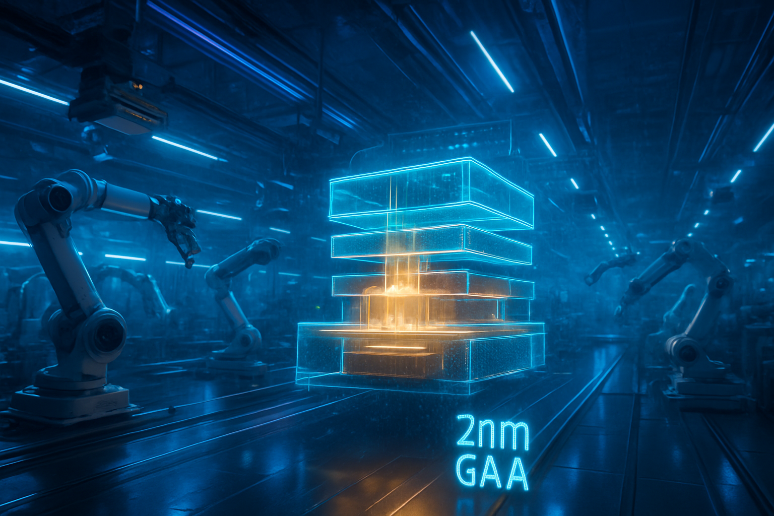
The implications of this development extend far beyond the laboratory. By leveraging "agentic" AI and high-fidelity virtual prototyping, Synopsys is enabling a "software-first" approach to engineering, particularly in the burgeoning field of software-defined vehicles (SDVs). As chips become more complex at the 2nm and sub-2nm nodes, the traditional bottlenecks of physical prototyping and manual verification are being replaced by AI-native workflows. This evolution is being fueled by a multi-billion dollar commitment from NVIDIA, which is increasingly treating Electronic Design Automation (EDA) not just as a tool, but as a core pillar of its own hardware dominance.
AgentEngineer and the Rise of Autonomous Chip Design
The technical centerpiece of Synopsys’ CES showcase was the introduction of AgentEngineer™, an agentic AI framework that marks the next evolution of the Synopsys.ai suite. Unlike previous AI tools that functioned as simple assistants, AgentEngineer utilizes autonomous AI agents capable of reasoning, planning, and executing complex engineering tasks with minimal human intervention. These agents can handle "high-toil" repetitive tasks such as design rule checking, layout optimization, and verification, allowing human engineers to focus on high-level architecture.
Synopsys also debuted its expanded virtualization portfolio, which integrates technology from its strategic acquisition of Ansys. This integration allows for the creation of "digital twins" of entire electronic stacks long before physical silicon exists. At the heart of this are new Virtualizer Development Kits (VDKs) designed for next-generation automotive architectures, including the Arm Zena compute subsystems and high-performance cores from NXP Semiconductors (NASDAQ: NXPI) and Texas Instruments (NASDAQ: TXN). By providing software teams with virtual System-on-Chip (SoC) models months in advance, Synopsys claims that the time for full system bring-up—once a grueling multi-month process—can now be completed in just a few days.
This approach differs radically from previous EDA methodologies, which relied heavily on "sequential" development—where software development waited for hardware prototypes. The new "shift-left" paradigm allows for parallel development, slashing the time-to-market for complex systems. Industry experts have noted that the integration of multiphysics simulation (heat, stress, and electromagnetics) directly into the AI design loop represents a breakthrough that was considered a "holy grail" only a few years ago.
NVIDIA’s $2 Billion Bet on the EDA Ecosystem
The industry's confidence in this AI-driven future was underscored by NVIDIA’s massive strategic investment. In a move that sent shockwaves through the market, NVIDIA has committed approximately $2 billion to expand its partnership with Synopsys, purchasing millions of shares and deepening technical integration. NVIDIA is no longer just a customer of EDA tools; it is co-architecting the infrastructure. By accelerating the Synopsys EDA stack with its own CUDA libraries and GPU clusters, NVIDIA is optimizing its upcoming GPU architectures—including the newly announced Rubin platform—using the very tools it is helping to build.
This partnership places significant pressure on other major players in the EDA space, such as Cadence Design Systems (NASDAQ: CDNS) and Siemens (OTC: SIEGY). At CES 2026, NVIDIA also announced an "Industrial AI Operating System" in collaboration with Siemens, which aims to bring generative and agentic workflows to the factory floor and PCB design. The competitive landscape is shifting from who has the best algorithms to who has the most integrated AI-native design stack backed by massive GPU compute power.
For tech giants and startups alike, this development creates a "winner-takes-most" dynamic. Companies that can afford to integrate these high-end, AI-driven EDA tools will be able to iterate on hardware at a pace that traditional competitors cannot match. Startups in the AI chip space, in particular, may find the 12-month reduction in design cycles to be their only path to survival in a market where hardware becomes obsolete in eighteen months.
A New Era of "Computers on Wheels" and 2nm Complexity
The wider significance of these advancements lies in their ability to solve the "complexity wall" of sub-2nm manufacturing. As transistors approach atomic scales, the physics of chip design becomes increasingly unpredictable. AI is the only tool capable of managing the quadrillions of design variables involved in modern lithography. NVIDIA’s cuLitho computational lithography library, integrated with Synopsys and TSMC (NYSE: TSM) workflows, has already reduced lithography simulation times from weeks to overnight, making the mass production of 2nm chips economically viable.
This shift is most visible in the automotive sector. The "software-defined vehicle" is no longer a buzzword; it is a necessity as cars transition into data centers on wheels. By virtualizing the entire vehicle electronics stack, Synopsys and its partners are reducing prototyping and testing costs by 20% to 60%. This fits into a broader trend where AI is being used to bridge the gap between the digital and physical worlds, a trend seen in other sectors like robotics and aerospace.
However, the move toward autonomous AI designers also raises concerns. Industry leaders have voiced caution regarding the "black box" nature of AI-generated designs and the potential for systemic errors that human engineers might overlook. Furthermore, the concentration of such powerful design tools in the hands of a few dominant players could lead to a bottleneck in global innovation if access is not democratized.
The Horizon: From Vera CPUs to Fully Autonomous Fab Integration
Looking forward, the next two years are expected to bring even deeper integration between AI reasoning and hardware manufacturing. Experts predict that NVIDIA’s Vera CPU—specifically designed for reasoning-heavy agentic AI—will become the primary engine for next-generation EDA workstations. These systems will likely move beyond "assisting" designers to proposing entire architectural configurations based on high-level performance goals, a concept known as "intent-based design."
The long-term goal is a closed-loop system where AI-driven EDA tools are directly linked to semiconductor fabrication plants (fabs). In this scenario, the design software would receive real-time telemetry from the manufacturing line, automatically adjusting chip layouts to account for minute variations in the production process. While challenges remain—particularly in the standardization of data across different vendors—the progress shown at CES 2026 suggests these hurdles are being cleared faster than anticipated.
Conclusion: The Acceleration of Human Ingenuity
The announcements from Synopsys and NVIDIA at CES 2026 mark a definitive end to the era of manual chip design. The ability to slash a year off the development cycle of a modern SoC is a feat of engineering that will ripple through every corner of the global economy, from faster smartphones to safer autonomous vehicles. The integration of agentic AI and virtual prototyping has turned the "shift-left" philosophy from a theoretical goal into a practical reality.
As we look toward the remainder of 2026, the industry will be watching closely to see how these tools perform in high-volume production environments. The true test will be the first wave of 2nm AI chips designed entirely within these new autonomous frameworks. For now, one thing is certain: the speed of innovation is no longer limited by how fast we can draw circuits, but by how fast we can train the AI to draw them for us.
This content is intended for informational purposes only and represents analysis of current AI developments.
TokenRing AI delivers enterprise-grade solutions for multi-agent AI workflow orchestration, AI-powered development tools, and seamless remote collaboration platforms.
For more information, visit https://www.tokenring.ai/.